EP0606001A2 - Verfahren zur Herstellung von Bipolar- und Feldeffekt-Transistoren - Google Patents
Verfahren zur Herstellung von Bipolar- und Feldeffekt-Transistoren Download PDFInfo
- Publication number
- EP0606001A2 EP0606001A2 EP19930310406 EP93310406A EP0606001A2 EP 0606001 A2 EP0606001 A2 EP 0606001A2 EP 19930310406 EP19930310406 EP 19930310406 EP 93310406 A EP93310406 A EP 93310406A EP 0606001 A2 EP0606001 A2 EP 0606001A2
- Authority
- EP
- European Patent Office
- Prior art keywords
- conductive layer
- layer
- forming
- area
- undercut
- Prior art date
- Legal status (The legal status is an assumption and is not a legal conclusion. Google has not performed a legal analysis and makes no representation as to the accuracy of the status listed.)
- Withdrawn
Links
- 238000000034 method Methods 0.000 title claims abstract description 44
- 230000005669 field effect Effects 0.000 title description 10
- 238000004519 manufacturing process Methods 0.000 title 1
- 239000012535 impurity Substances 0.000 claims abstract description 37
- 239000002019 doping agent Substances 0.000 claims abstract description 21
- 238000005530 etching Methods 0.000 claims abstract description 12
- 230000003647 oxidation Effects 0.000 claims abstract description 5
- 238000007254 oxidation reaction Methods 0.000 claims abstract description 5
- 239000004065 semiconductor Substances 0.000 claims description 32
- 239000000126 substance Substances 0.000 claims description 22
- 239000000758 substrate Substances 0.000 claims description 13
- 230000002093 peripheral effect Effects 0.000 claims description 6
- 238000000151 deposition Methods 0.000 claims description 5
- 238000010438 heat treatment Methods 0.000 claims description 3
- 239000004020 conductor Substances 0.000 claims description 2
- 238000009792 diffusion process Methods 0.000 claims description 2
- FGUUSXIOTUKUDN-IBGZPJMESA-N C1(=CC=CC=C1)N1C2=C(NC([C@H](C1)NC=1OC(=NN=1)C1=CC=CC=C1)=O)C=CC=C2 Chemical compound C1(=CC=CC=C1)N1C2=C(NC([C@H](C1)NC=1OC(=NN=1)C1=CC=CC=C1)=O)C=CC=C2 FGUUSXIOTUKUDN-IBGZPJMESA-N 0.000 claims 3
- 230000001590 oxidative effect Effects 0.000 claims 1
- 229910021420 polycrystalline silicon Inorganic materials 0.000 abstract description 69
- 229920005591 polysilicon Polymers 0.000 abstract description 69
- VYPSYNLAJGMNEJ-UHFFFAOYSA-N Silicium dioxide Chemical compound O=[Si]=O VYPSYNLAJGMNEJ-UHFFFAOYSA-N 0.000 description 29
- 229910052814 silicon oxide Inorganic materials 0.000 description 29
- KRHYYFGTRYWZRS-UHFFFAOYSA-N Fluorane Chemical compound F KRHYYFGTRYWZRS-UHFFFAOYSA-N 0.000 description 10
- XUIMIQQOPSSXEZ-UHFFFAOYSA-N Silicon Chemical compound [Si] XUIMIQQOPSSXEZ-UHFFFAOYSA-N 0.000 description 9
- 229910052710 silicon Inorganic materials 0.000 description 8
- 239000010703 silicon Substances 0.000 description 8
- ZOXJGFHDIHLPTG-UHFFFAOYSA-N Boron Chemical compound [B] ZOXJGFHDIHLPTG-UHFFFAOYSA-N 0.000 description 7
- 229910052796 boron Inorganic materials 0.000 description 7
- 229910052581 Si3N4 Inorganic materials 0.000 description 5
- HQVNEWCFYHHQES-UHFFFAOYSA-N silicon nitride Chemical compound N12[Si]34N5[Si]62N3[Si]51N64 HQVNEWCFYHHQES-UHFFFAOYSA-N 0.000 description 5
- 238000004151 rapid thermal annealing Methods 0.000 description 4
- 230000015572 biosynthetic process Effects 0.000 description 3
- 238000002161 passivation Methods 0.000 description 3
- 238000002360 preparation method Methods 0.000 description 3
- OAICVXFJPJFONN-UHFFFAOYSA-N Phosphorus Chemical compound [P] OAICVXFJPJFONN-UHFFFAOYSA-N 0.000 description 2
- 239000005388 borosilicate glass Substances 0.000 description 2
- 230000010354 integration Effects 0.000 description 2
- 229910052698 phosphorus Inorganic materials 0.000 description 2
- 239000011574 phosphorus Substances 0.000 description 2
- 229910052785 arsenic Inorganic materials 0.000 description 1
- RQNWIZPPADIBDY-UHFFFAOYSA-N arsenic atom Chemical compound [As] RQNWIZPPADIBDY-UHFFFAOYSA-N 0.000 description 1
- 230000015556 catabolic process Effects 0.000 description 1
- 239000013078 crystal Substances 0.000 description 1
- 230000007423 decrease Effects 0.000 description 1
- 230000007547 defect Effects 0.000 description 1
- 230000008021 deposition Effects 0.000 description 1
- 238000002513 implantation Methods 0.000 description 1
- 238000012986 modification Methods 0.000 description 1
- 230000004048 modification Effects 0.000 description 1
- 230000003071 parasitic effect Effects 0.000 description 1
- 230000001105 regulatory effect Effects 0.000 description 1
Images


Classifications
-
- H—ELECTRICITY
- H01—ELECTRIC ELEMENTS
- H01L—SEMICONDUCTOR DEVICES NOT COVERED BY CLASS H10
- H01L29/00—Semiconductor devices adapted for rectifying, amplifying, oscillating or switching, or capacitors or resistors with at least one potential-jump barrier or surface barrier, e.g. PN junction depletion layer or carrier concentration layer; Details of semiconductor bodies or of electrodes thereof ; Multistep manufacturing processes therefor
- H01L29/66—Types of semiconductor device ; Multistep manufacturing processes therefor
- H01L29/66007—Multistep manufacturing processes
- H01L29/66075—Multistep manufacturing processes of devices having semiconductor bodies comprising group 14 or group 13/15 materials
- H01L29/66227—Multistep manufacturing processes of devices having semiconductor bodies comprising group 14 or group 13/15 materials the devices being controllable only by the electric current supplied or the electric potential applied, to an electrode which does not carry the current to be rectified, amplified or switched, e.g. three-terminal devices
- H01L29/66234—Bipolar junction transistors [BJT]
- H01L29/6625—Lateral transistors
-
- H—ELECTRICITY
- H01—ELECTRIC ELEMENTS
- H01L—SEMICONDUCTOR DEVICES NOT COVERED BY CLASS H10
- H01L21/00—Processes or apparatus adapted for the manufacture or treatment of semiconductor or solid state devices or of parts thereof
- H01L21/02—Manufacture or treatment of semiconductor devices or of parts thereof
- H01L21/04—Manufacture or treatment of semiconductor devices or of parts thereof the devices having at least one potential-jump barrier or surface barrier, e.g. PN junction, depletion layer or carrier concentration layer
- H01L21/18—Manufacture or treatment of semiconductor devices or of parts thereof the devices having at least one potential-jump barrier or surface barrier, e.g. PN junction, depletion layer or carrier concentration layer the devices having semiconductor bodies comprising elements of Group IV of the Periodic System or AIIIBV compounds with or without impurities, e.g. doping materials
- H01L21/22—Diffusion of impurity materials, e.g. doping materials, electrode materials, into or out of a semiconductor body, or between semiconductor regions; Interactions between two or more impurities; Redistribution of impurities
- H01L21/225—Diffusion of impurity materials, e.g. doping materials, electrode materials, into or out of a semiconductor body, or between semiconductor regions; Interactions between two or more impurities; Redistribution of impurities using diffusion into or out of a solid from or into a solid phase, e.g. a doped oxide layer
- H01L21/2251—Diffusion into or out of group IV semiconductors
- H01L21/2254—Diffusion into or out of group IV semiconductors from or through or into an applied layer, e.g. photoresist, nitrides
- H01L21/2257—Diffusion into or out of group IV semiconductors from or through or into an applied layer, e.g. photoresist, nitrides the applied layer being silicon or silicide or SIPOS, e.g. polysilicon, porous silicon
-
- H—ELECTRICITY
- H01—ELECTRIC ELEMENTS
- H01L—SEMICONDUCTOR DEVICES NOT COVERED BY CLASS H10
- H01L29/00—Semiconductor devices adapted for rectifying, amplifying, oscillating or switching, or capacitors or resistors with at least one potential-jump barrier or surface barrier, e.g. PN junction depletion layer or carrier concentration layer; Details of semiconductor bodies or of electrodes thereof ; Multistep manufacturing processes therefor
- H01L29/02—Semiconductor bodies ; Multistep manufacturing processes therefor
- H01L29/06—Semiconductor bodies ; Multistep manufacturing processes therefor characterised by their shape; characterised by the shapes, relative sizes, or dispositions of the semiconductor regions ; characterised by the concentration or distribution of impurities within semiconductor regions
- H01L29/10—Semiconductor bodies ; Multistep manufacturing processes therefor characterised by their shape; characterised by the shapes, relative sizes, or dispositions of the semiconductor regions ; characterised by the concentration or distribution of impurities within semiconductor regions with semiconductor regions connected to an electrode not carrying current to be rectified, amplified or switched and such electrode being part of a semiconductor device which comprises three or more electrodes
- H01L29/1004—Base region of bipolar transistors
-
- H—ELECTRICITY
- H01—ELECTRIC ELEMENTS
- H01L—SEMICONDUCTOR DEVICES NOT COVERED BY CLASS H10
- H01L29/00—Semiconductor devices adapted for rectifying, amplifying, oscillating or switching, or capacitors or resistors with at least one potential-jump barrier or surface barrier, e.g. PN junction depletion layer or carrier concentration layer; Details of semiconductor bodies or of electrodes thereof ; Multistep manufacturing processes therefor
- H01L29/40—Electrodes ; Multistep manufacturing processes therefor
- H01L29/43—Electrodes ; Multistep manufacturing processes therefor characterised by the materials of which they are formed
- H01L29/45—Ohmic electrodes
- H01L29/456—Ohmic electrodes on silicon
-
- H—ELECTRICITY
- H01—ELECTRIC ELEMENTS
- H01L—SEMICONDUCTOR DEVICES NOT COVERED BY CLASS H10
- H01L29/00—Semiconductor devices adapted for rectifying, amplifying, oscillating or switching, or capacitors or resistors with at least one potential-jump barrier or surface barrier, e.g. PN junction depletion layer or carrier concentration layer; Details of semiconductor bodies or of electrodes thereof ; Multistep manufacturing processes therefor
- H01L29/66—Types of semiconductor device ; Multistep manufacturing processes therefor
- H01L29/66007—Multistep manufacturing processes
- H01L29/66075—Multistep manufacturing processes of devices having semiconductor bodies comprising group 14 or group 13/15 materials
- H01L29/66227—Multistep manufacturing processes of devices having semiconductor bodies comprising group 14 or group 13/15 materials the devices being controllable only by the electric current supplied or the electric potential applied, to an electrode which does not carry the current to be rectified, amplified or switched, e.g. three-terminal devices
- H01L29/66234—Bipolar junction transistors [BJT]
- H01L29/66272—Silicon vertical transistors
-
- H—ELECTRICITY
- H01—ELECTRIC ELEMENTS
- H01L—SEMICONDUCTOR DEVICES NOT COVERED BY CLASS H10
- H01L29/00—Semiconductor devices adapted for rectifying, amplifying, oscillating or switching, or capacitors or resistors with at least one potential-jump barrier or surface barrier, e.g. PN junction depletion layer or carrier concentration layer; Details of semiconductor bodies or of electrodes thereof ; Multistep manufacturing processes therefor
- H01L29/66—Types of semiconductor device ; Multistep manufacturing processes therefor
- H01L29/66007—Multistep manufacturing processes
- H01L29/66075—Multistep manufacturing processes of devices having semiconductor bodies comprising group 14 or group 13/15 materials
- H01L29/66227—Multistep manufacturing processes of devices having semiconductor bodies comprising group 14 or group 13/15 materials the devices being controllable only by the electric current supplied or the electric potential applied, to an electrode which does not carry the current to be rectified, amplified or switched, e.g. three-terminal devices
- H01L29/66409—Unipolar field-effect transistors
- H01L29/66477—Unipolar field-effect transistors with an insulated gate, i.e. MISFET
- H01L29/66568—Lateral single gate silicon transistors
- H01L29/66606—Lateral single gate silicon transistors with final source and drain contacts formation strictly before final or dummy gate formation, e.g. contact first technology
Definitions
- This invention relates to a process of fabricating a semiconductor device and, more particularly, to a process of fabricating a miniature transistor on a semiconductor substrate.
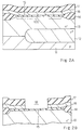
- the prior art process sequence starts with preparation of a silicon substrate having a lightly doped n-type epitaxial layer 1, and a thick field oxide layer 2 is selectively grown on the major surface of the lightly doped n-type epitaxial layer 1.
- the thick field oxide layer 2 exposes an active area, and a silicon oxide layer 3 is thermally grown in the active area to thickness of 400 to 600 angstroms.
- a polysilicon layer 4 is deposited over the entire surface of the structure to thickness of 2500 angstroms to 3500 angstroms, and boron is introduced into the polysilicon layer 4.
- a silicon nitride layer 5 is deposited on the polysilicon layer 4 to thickness of 2000 to 3000 angstroms, and the doped polysilicon layer 4 and the silicon nitride layer 5 are partially etched away through an anisotropical etching technique so as to expose a part of the silicon oxide layer 3 over an area assigned to emitter and base regions.
- the resultant structure of this stage is illustrated in Fig. 1A.
- Dilute hydrofluoric acid is applied, and the dilute hydrofluoric acid etches away the exposed silicon oxide layer 3.
- the hydrofluoric acid further etches away the silicon oxide layer 3 beneath the periphery of the doped polysilicon layer 4, and an undercut 3a as wide as 1000 angstroms takes place.
- Polysilicon is, thereafter, deposited over the entire surface of the structure to thickness of 200 to 300 angstroms, and the undercut 3a is buried in the polysilicon layer 6 as shown in fig. 1B.
- the structure is placed in high temperature ambience, and the polysilicon layer 6 is thermally oxidized. Most of the polysilicon layer 6 is converted to a silicon oxide layer 7. However, the polysilicon layer 6 is left in the undercut 3a. While the polysilicon layer 6 is being thermally oxidized, the boron doped into the polysilicon layer 4 is diffused through the polysilicon 6 into the epitaxial layer 1, and p-type base contact region 8 is formed in the lightly doped n-type epitaxial layer 1 as shown in Fig. 1C.
- the silicon oxide layer 7 is anisotropically etched, and is partially left on the periphery of the silicon nitride layer 5 and on the periphery of the polysilicon layer 4.
- the silicon oxide thus left on the peripheries serves as a side wall 7a, and isolates the base contact region 8 and the doped polysilicon layer 4 from an emitter region.
- P-type impurity is introduced into an area surrounded by the base contact region 8, and a p-type base region 9 is formed inside of the base contact region 8.
- a phosphorus or arsenic-doped polysilicon is patterned to an emitter electrode 10, and the phosphorus or the arsenic is diffused from the doped polysilicon layer for forming an emitter region 11.
- the resultant structure is illustrated in Fig. 1D.
- the prior art bipolar transistor is enlarged, and the integration density is hardly increased.
- the large base contact region 8 is causative of a large amount of parasitic capacitance between the base and the collector, and decreases the breakdown voltage between the emitter and the base.
- Another problem inherent in the prior art process is a stress due to the silicon oxide converted from the polysilicon.
- the silicon oxide is increased in volume, and the silicon oxide layer 7 presses the lightly doped n-type epitaxial layer 1 beneath the undercut 3a.
- the stress is causative of crystal defects of the lightly doped n-type epitaxial layer 1 beneath the undercut 3a, and the base contact region 6 suffers from leakage current. The leakage current deteriorates the transistor characteristics.
- the present invention proposes to leave a piece of semiconductor substance in an undercut by means of an etching process.
- an undercut is formed beneath a periphery of a doped conductive layer over an active area, and a piece of a second semiconductor substance is disposed in the undercut for diffusing a dopant impurity from the first semiconductor layer through the second semiconductor substance into the active area, characterised by depositing said second conductor substance as a layer over a surface to which the undercut is open, so as to fill the undercut with the second semiconductor substance, and removing said layer except in the undercut by etching without oxidation.
- a process of fabricating a transistor on a semiconductor substrate comprising the steps of: a) forming a multi-layered structure of a first insulating layer on an active area defined in a major surface of the semiconductor substrate, a first conductive layer of a semiconductor substance doped with a first dopant impurity and formed on the first insulating layer and a second insulating layer formed on the first conductive layer; b) partially removing the second insulating layer and the first conductive layer for forming a hole exposing a first part of the first insulating layer in a central sub-area of the active area; c) etching the first part of the first insulating layer and a second part of the first insulating layer contiguous to the first part and overlain by a periphery of the first conductive layer for forming an undercut beneath the periphery of the first conductive layer; d) depositing a second conductive layer of the semiconductor substance over the entire
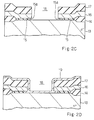
- a process sequence for fabricating a miniature bipolar transistor embodying the present invention starts with preparation of a lightly doped p-type silicon substrate 11 shown in Fig. 2A.
- An n-type impurity is selectively diffused in major surface portion of the p-type silicon substrate 11 for forming a heavily doped n-type buried layer 12, and lightly doped n-type silicon is epitaxially grown over the p-type silicon substrate 11 and the heavily doped n-type buried layer 12 to thickness of 0.6 micron.
- the lightly doped n-type silicon forms a lightly doped epitaxial layer 13, and the lightly doped epitaxial layer 13 is about 1 ohm-cm.
- the lightly doped n-type epitaxial layer 13 is partially oxidized, and a field oxide layer 14 is grown to thickness of 0.1 to 1.5 microns.
- the field oxide layer 14 defines an active area 100 assigned to a bipolar transistor, and the active area 100 is thermally oxidized so that a silicon oxide layer 15 covers the active area 100.
- the silicon oxide layer 15 ranges from 20 to 100 nanometers in thickness, and the thickness between 40 to 60 nanometers is desirable.
- a p-type polysilicon layer 16 is deposited to thickness 0.1 to 0.4 micron over the entire surface of the structure, and an insulating layer 17 of, for example, silicon nitride is deposited on the p-type polysilicon layer 16 to thickness of 0.15 to 0.40 micron.
- the resultant structure of this stage is illustrated in Fig. 2A.
- a hole 18 exposes the part of the silicon oxide layer 15 disposed over a central area assigned to base and emitter regions of the bipolar transistor.
- Dilute hydrofluoric acid is applied to the exposed portion of the silicon oxide layer 15. Then, the exposed portion of the silicon oxide layer 15 is etched away in the dilute hydrofluoric acid, and the etching proceeds to the silicon oxide layer beneath the periphery of the p-type polysilicon layer 15. As a result, an undercut 15a is produced beneath the periphery of the p-type silicon oxide layer 16, and the silicon oxide layer 15 is retracted from the inner periphery of the p-type polysilicon layer 16 by 0.1 micron.
- Fig. 2C illustrates the resultant structure at this stage.
- a polysilicon layer 19 is deposited over the entire surface of the structure to thickness not less than a half of the thickness of the silicon oxide layer 15, and the undercut 15a is buried in the polysilicon layer 19 as shown in Fig. 2D.
- the polysilicon layer 19 is exposed to a low-energy radical etchant such as, for example, CF4, and the polysilicon layer 19 is removed. However, a part 19a of the polysilicon layer 19 is left in the undercut 15a, and the low-energy radical etchant does not damage the exposed lightly doped n-type epitaxial layer 13.
- a low-energy radical etchant such as, for example, CF4
- Boron is ion-implanted through the hole 18 into the lightly doped n-type epitaxial layer 13 at dose of 2 x 1013 cm ⁇ 2 under the implantation energy at 10 keV, and a p-type base region 20 is formed in the lightly doped n-type epitaxial layer 13.
- the p-type base region 20 may form through another sequence. Namely, a boro-silicate glass film containing boron at 5 mol% is deposited over the entire surface to thickness of 0.1 micron, and is held in contact with the exposed area of the lightly doped n-type epitaxial layer 13. The boro-silicate glass film is heated to 1000 degrees in centigrade through a rapid thermal annealing technique, and is maintained for 20 seconds. Then, the boron is diffused into the lightly doped n-type epitaxial layer 13, and forms the p-type base region 20.
- an insulating layer is deposited over the entire surface of the structure, and is anisotropically etched away so that a side wall is left on the periphery of the silicon oxide layer 17 and on the periphery of the doped polysilicon layer 16 as shown in Fig. 2F.
- the side wall 21 electrically isolates the doped polysilicon layer 16 from an emitter electrode.
- n-type doped polysilicon is deposited over the entire surface of the structure, and the n-type doped polysilicon is patterned to an emitter electrode 22.
- the emitter electrode 22 is held in contact with a central area of the base region 20.
- the n-type impurity is diffused from the emitter electrode 22 into the central area of the base region 20, and an n-type emitter region 23 is formed in and nested with the p-type base region 20.
- the n-type impurity is diffused from the doped polysilicon layer 16 through the part 19a of polysilicon into the lightly doped n-type epitaxial layer 13, and a base contact region 24 is partially overlapped with the base region 20 as shown in Fig. 2G.
- Fig. 3 which illustrates the relationship in arrangement among the polysilicon layer 16, the side wall 21 and the active area 100.
- Figs. 2A to 2G are taken along line A-A in Fig. 3.
- the process sequence according to the present invention leaves the polysilicon 19a through an etching process, and any stress is not exerted on the lightly doped n-type epitaxial layer 13. This results in an extremely small amount of leakage current and, improves the transistor characteristics.
- the base contact region 24 is simultaneously formed together with the emitter region 23 at the later stage thereof, and does not expand over an expected area. This results in a small amount of occupation area, and increases the integration density of an integrated circuit device.
- the present invention is applicable for a process of fabricating a field effect transistor, and the process sequence is described hereinbelow.
- Figs. 4A to 4C are cross sectional views taken along line D-D of Fig. 5.
- the process for fabricating a field effect transistor starts with preparation of a p-type silicon substrate 31, and a lightly doped n-type epitaxial layer 32 is grown on the p-type silicon substrate 31.
- a field oxide layer 33 is selectively grown on the lightly doped n-type epitaxial layer 32, and defines an active area assigned to a MIS (Metal-Insulator-Semiconductor) field effect transistor.
- the active area is, thereafter, thermally oxidized, and a silicon oxide layer 34 covers the active area.
- a p-type doped polysilicon layer 35 is deposited over the entire surface of the structure, and an insulating layer 36 is, thereafter, deposited over the p-type polysilicon layer 35.
- the resultant structure at this stage is analogous to that shown in Fig. 2A.
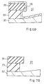
- the insulating layer 36 and the p-type polysilicon layer 35 are partially etched away for forming an opening 37 as similar to that shown in Fig. 2B.
- the opening 37 is wider than the p-type polysilicon layer 35, and, accordingly, the p-type polysilicon layer 35 is split into two parts 35a and 35b.
- the opening 37 is shorter than the length of the active area, and the leading end portions of the two parts 35a and 35b are on the silicon oxide layer 34. A central portion of the silicon oxide layer 34 is exposed to the opening 37.
- Polysilicon is, thereafter, deposited over the entire surface, and fills the undercuts 34a.
- the thickness of the polysilicon layer 38 thus deposited is regulated to be not less than a half of the silicon oxide layer 34 and is less than a third of the field oxide layer 33. For this reason, polysilicon layer 38 fills the undercuts 34a beneath the leading end portions of the p-type polysilicon layer 35 as shown in Fig. 6A, but is topological along the field oxide layer 33 as shown in Fig. 6B.
- the polysilicon layer 38 is isotropically etched away until the p-type polysilicon layer 35 is exposed, and pieces of polysilicon 38a are left in the undercuts 34a as shown in Fig. 7A. However, the polysilicon layer 38 is perfectly etched away from the side surface of the field oxide layer 33 as shown in Fig. 7B. The resultant structure at this stage is analogous to that shown in Fig. 2E.
- insulating substance is deposited over the entire surface of the structure, and the insulating layer is anisotropically etched away until a central sub-area of the active area is exposed again. Then, a side wall 39 is left along the periphery of the opening 37, and the secondary opening 37a exposes the central sub-area as shown in Fig. 4A.
- the resultant structure is placed in high-temperature wet ambience at 750 degrees in centigrade, and the central sub-area is thermally oxidized.
- the silicon oxide layer 40 thus thermally oxidized is 10 to 20 nanometers in thickness.
- the silicon oxide layer 40 serves as a gate insulating film of the MIS type field effect transistor.
- p-type impurity is diffused from the p-type polysilicon layer 35 through the pieces of polysilicon 38a into the lightly doped n-type epitaxial layer 32, and source and drain regions 41a and 41b are formed in the lightly doped n-type epitaxial layer 32.
- the resultant structure at this stage is illustrated in Fig. 4B.
- a heavily doped polysilicon is deposited over the entire surface of the structure, and is patterned into a gate electrode 42 as shown in Fig. 4C.
- the source and drain regions 41a and 41b are formed simultaneously with the gate insulating film 40, and are hardly diffused over expected areas, because a large amount of heat is not subjected to the source and drain regions 41a and 41b. This results in a miniature MIS type field effect transistor.
- a p-channel type MIS field effect transistor is fabricated through the process sequence according to the present invention.
- the present invention is applicable to a process of fabricating a lateral bipolar transistor.
- the process sequence implementing the third embodiment is similar to that of the second embodiment until the insulating side wall 39 is patterned on the side surfaces, and the component layers and regions are labeled with the same references designating the corresponding layers and regions of the second embodiment.
- p-type doped polysilicon 35 After the formation of the insulating side wall 39, heat is applied to the p-type doped polysilicon 35, and p-type dopant impurity such as, for example, boron is diffused through the pieces of polysilicon 38a and 38b into the lightly doped n-type epitaxial layer 32 for forming emitter and collector regions 50 and 51.
- p-type dopant impurity such as, for example, boron is diffused through the pieces of polysilicon 38a and 38b into the lightly doped n-type epitaxial layer 32 for forming emitter and collector regions 50 and 51.
- n-type doped polysilicon layer is deposited over the entire surface of the structure, and is patterned into a base electrode 52.
- the base electrode 52 is heated through a rapid thermal annealing, and the n-type dopant impurity is diffused from the base electrode 52 into the lightly doped n-type epitaxial layer 32.
- the n-type dopant impurity thus diffused forms a base contact region 53 as shown in Fig. 8B.
- the rapid thermal annealing only have small influence on the emitter region 50 and the collector region 51, and the lateral bipolar transistor can be scaled down.
- a passivation layer covers the structure, and a lateral bipolar transistor with the emitter, base and collector electrodes 35b, 52 and 35a is completed.
- Fig. 9 illustrates the layout of the lateral bipolar transistor, and the structure shown in Figs. 8A and 8B are taken along line E-E of Fig. 9.
- an n-p-n type lateral bipolar transistor is formed by replacing the p-type doped polysilicon 35 and the n-type base electrode 52 with an n-type doped polysilicon and a p-type base electrode.
- the emitter region 50 and the collector region 51 are not expanded over expected areas, and a miniature lateral bipolar transistor is fabricated through the process sequence according to the present invention.
- any p-type dopant impurity and any n-type dopant impurity may be available, and the dimensions do not set any limit on the present invention.
- silicon nitride layers may be available instead of silicon oxide layers.
Applications Claiming Priority (2)
| Application Number | Priority Date | Filing Date | Title |
|---|---|---|---|
| JP35870292A JPH0793316B2 (ja) | 1992-12-28 | 1992-12-28 | 半導体装置の製造方法 |
| JP358702/92 | 1992-12-28 |
Publications (1)
| Publication Number | Publication Date |
|---|---|
| EP0606001A2 true EP0606001A2 (de) | 1994-07-13 |
Family
ID=18460676
Family Applications (1)
| Application Number | Title | Priority Date | Filing Date |
|---|---|---|---|
| EP19930310406 Withdrawn EP0606001A2 (de) | 1992-12-28 | 1993-12-22 | Verfahren zur Herstellung von Bipolar- und Feldeffekt-Transistoren |
Country Status (3)
| Country | Link |
|---|---|
| EP (1) | EP0606001A2 (de) |
| JP (1) | JPH0793316B2 (de) |
| KR (1) | KR970004451B1 (de) |
Cited By (8)
| Publication number | Priority date | Publication date | Assignee | Title |
|---|---|---|---|---|
| EP0734073A2 (de) * | 1995-03-23 | 1996-09-25 | Texas Instruments Incorporated | Bipolartransistor und Verfahren zur Herstellung |
| EP0843350A1 (de) * | 1996-11-19 | 1998-05-20 | STMicroelectronics S.A. | Bipolartransistor mit einem nicht homogenen Emitter in einer BICMOS integrierter Schaltung |
| GB2327296A (en) * | 1997-07-14 | 1999-01-20 | United Microelectronics Corp | Reverse self aligned narrow gate fet |
| DE19742624A1 (de) * | 1997-09-26 | 1999-04-22 | Siemens Ag | Herstellverfahren für einen vertikalen Bipolartransistor |
| US6156594A (en) * | 1996-11-19 | 2000-12-05 | Sgs-Thomson Microelectronics S.A. | Fabrication of bipolar/CMOS integrated circuits and of a capacitor |
| US6713361B2 (en) * | 2000-09-27 | 2004-03-30 | Texas Instruments Incorporated | Method of manufacturing a bipolar junction transistor including undercutting regions adjacent to the emitter region to enlarge the emitter region |
| EP0709896B1 (de) * | 1994-10-26 | 2004-08-25 | Consorzio per la Ricerca sulla Microelettronica nel Mezzogiorno - CoRiMMe | Verfahren zur Herstellung eines lateralen PNP-Hochfrequenztransistors |
| US8190802B2 (en) | 2006-08-25 | 2012-05-29 | Atomia Oy | Circuit, method and arrangement for implementing simple and reliable distributed arbitration on a bus |
Families Citing this family (2)
| Publication number | Priority date | Publication date | Assignee | Title |
|---|---|---|---|---|
| KR20210143351A (ko) | 2020-05-19 | 2021-11-29 | 주식회사 엠오피(M.O.P Co., Ltd.) | 관형 유체 혼합기 및 이의 제조방법 |
| KR20230019359A (ko) | 2021-07-30 | 2023-02-08 | 주식회사 엠오피(M.O.P Co., Ltd.) | 관형 유체 혼합기 및 이의 제조방법 |
-
1992
- 1992-12-28 JP JP35870292A patent/JPH0793316B2/ja not_active Expired - Lifetime
-
1993
- 1993-12-22 EP EP19930310406 patent/EP0606001A2/de not_active Withdrawn
- 1993-12-28 KR KR93031749A patent/KR970004451B1/ko active IP Right Grant
Cited By (12)
| Publication number | Priority date | Publication date | Assignee | Title |
|---|---|---|---|---|
| EP0709896B1 (de) * | 1994-10-26 | 2004-08-25 | Consorzio per la Ricerca sulla Microelettronica nel Mezzogiorno - CoRiMMe | Verfahren zur Herstellung eines lateralen PNP-Hochfrequenztransistors |
| EP0734073A2 (de) * | 1995-03-23 | 1996-09-25 | Texas Instruments Incorporated | Bipolartransistor und Verfahren zur Herstellung |
| EP0734073A3 (de) * | 1995-03-23 | 1996-12-04 | Texas Instruments Inc | Bipolartransistor und Verfahren zur Herstellung |
| EP0843350A1 (de) * | 1996-11-19 | 1998-05-20 | STMicroelectronics S.A. | Bipolartransistor mit einem nicht homogenen Emitter in einer BICMOS integrierter Schaltung |
| FR2756100A1 (fr) * | 1996-11-19 | 1998-05-22 | Sgs Thomson Microelectronics | Transistor bipolaire a emetteur inhomogene dans un circuit integre bicmos |
| US6156594A (en) * | 1996-11-19 | 2000-12-05 | Sgs-Thomson Microelectronics S.A. | Fabrication of bipolar/CMOS integrated circuits and of a capacitor |
| US6180442B1 (en) | 1996-11-19 | 2001-01-30 | Sgs-Thomson Microelectronics S.A. | Bipolar transistor with an inhomogeneous emitter in a BICMOS integrated circuit method |
| GB2327296A (en) * | 1997-07-14 | 1999-01-20 | United Microelectronics Corp | Reverse self aligned narrow gate fet |
| GB2327296B (en) * | 1997-07-14 | 1999-06-16 | United Microelectronics Corp | Method of making a FET |
| DE19742624A1 (de) * | 1997-09-26 | 1999-04-22 | Siemens Ag | Herstellverfahren für einen vertikalen Bipolartransistor |
| US6713361B2 (en) * | 2000-09-27 | 2004-03-30 | Texas Instruments Incorporated | Method of manufacturing a bipolar junction transistor including undercutting regions adjacent to the emitter region to enlarge the emitter region |
| US8190802B2 (en) | 2006-08-25 | 2012-05-29 | Atomia Oy | Circuit, method and arrangement for implementing simple and reliable distributed arbitration on a bus |
Also Published As
| Publication number | Publication date |
|---|---|
| JPH0793316B2 (ja) | 1995-10-09 |
| KR970004451B1 (en) | 1997-03-27 |
| JPH06204235A (ja) | 1994-07-22 |
Similar Documents
| Publication | Publication Date | Title |
|---|---|---|
| US4757032A (en) | Method for DMOS semiconductor device fabrication | |
| US5171702A (en) | Method for forming a thick base oxide in a BiCMOS process | |
| US4839305A (en) | Method of making single polysilicon self-aligned transistor | |
| EP0252206A2 (de) | Verfahren zum Herstellen einer Halbleiterstruktur | |
| US6238985B1 (en) | Semiconductor device and method for fabricating the same | |
| EP0606001A2 (de) | Verfahren zur Herstellung von Bipolar- und Feldeffekt-Transistoren | |
| JPH1116921A (ja) | 半導体装置 | |
| EP0274217A1 (de) | Verfahren zum Herstellen einer Halbleitervorrichtung | |
| US5395782A (en) | Process for fabricating a semiconductor integrated circuit | |
| JP2908715B2 (ja) | モスフェット(mosfet)及びその製造方法 | |
| US6451645B1 (en) | Method for manufacturing semiconductor device with power semiconductor element and diode | |
| JP2001023998A (ja) | セルフアライン型ベース−エミッタ接合を有するバイポーラ素子の製造方法 | |
| US5747374A (en) | Methods of fabricating bipolar transistors having separately formed intrinsic base and link-up regions | |
| US5148252A (en) | Bipolar transistor | |
| US5188972A (en) | Method for making bipolar transistor by self-aligning the emitter to the base contact diffusion | |
| JP2624948B2 (ja) | Mos−fet製造方法 | |
| EP0406883B1 (de) | Bipolare Halbleitervorrichtung und Verfahren zu deren Herstellung | |
| US5049512A (en) | Method of forming a MOS field-effect transistor | |
| JP3190370B2 (ja) | 密接して離隔したコンタクトを有するBiCMOS装置及びその製造方法 | |
| JP3280734B2 (ja) | 半導体装置及びその製造方法 | |
| JP2917646B2 (ja) | 半導体集積回路装置の製造方法 | |
| US5950080A (en) | Semiconductor device and method of manufacturing the same | |
| JP2910640B2 (ja) | 半導体装置およびその製造方法 | |
| JP2722506B2 (ja) | 半導体装置及びその製造方法 | |
| JP2890550B2 (ja) | 半導体装置の製造方法 |
Legal Events
| Date | Code | Title | Description |
|---|---|---|---|
| PUAI | Public reference made under article 153(3) epc to a published international application that has entered the european phase |
Free format text: ORIGINAL CODE: 0009012 |
|
| AK | Designated contracting states |
Kind code of ref document: A2 Designated state(s): DE FR GB |
|
| STAA | Information on the status of an ep patent application or granted ep patent |
Free format text: STATUS: THE APPLICATION HAS BEEN WITHDRAWN |
|
| 18W | Application withdrawn |
Withdrawal date: 19950630 |
|
| R18W | Application withdrawn (corrected) |
Effective date: 19950630 |