EP0604231A1 - Semiconductor device applicable for liquid crystal display device, and process for its fabrication - Google Patents
Semiconductor device applicable for liquid crystal display device, and process for its fabrication Download PDFInfo
- Publication number
- EP0604231A1 EP0604231A1 EP93310476A EP93310476A EP0604231A1 EP 0604231 A1 EP0604231 A1 EP 0604231A1 EP 93310476 A EP93310476 A EP 93310476A EP 93310476 A EP93310476 A EP 93310476A EP 0604231 A1 EP0604231 A1 EP 0604231A1
- Authority
- EP
- European Patent Office
- Prior art keywords
- substrate
- semiconductor
- monocrystalline
- film
- liquid crystal
- Prior art date
- Legal status (The legal status is an assumption and is not a legal conclusion. Google has not performed a legal analysis and makes no representation as to the accuracy of the status listed.)
- Granted
Links
Images


Classifications
-
- G—PHYSICS
- G02—OPTICS
- G02F—OPTICAL DEVICES OR ARRANGEMENTS FOR THE CONTROL OF LIGHT BY MODIFICATION OF THE OPTICAL PROPERTIES OF THE MEDIA OF THE ELEMENTS INVOLVED THEREIN; NON-LINEAR OPTICS; FREQUENCY-CHANGING OF LIGHT; OPTICAL LOGIC ELEMENTS; OPTICAL ANALOGUE/DIGITAL CONVERTERS
- G02F1/00—Devices or arrangements for the control of the intensity, colour, phase, polarisation or direction of light arriving from an independent light source, e.g. switching, gating or modulating; Non-linear optics
- G02F1/01—Devices or arrangements for the control of the intensity, colour, phase, polarisation or direction of light arriving from an independent light source, e.g. switching, gating or modulating; Non-linear optics for the control of the intensity, phase, polarisation or colour
- G02F1/13—Devices or arrangements for the control of the intensity, colour, phase, polarisation or direction of light arriving from an independent light source, e.g. switching, gating or modulating; Non-linear optics for the control of the intensity, phase, polarisation or colour based on liquid crystals, e.g. single liquid crystal display cells
- G02F1/133—Constructional arrangements; Operation of liquid crystal cells; Circuit arrangements
- G02F1/1333—Constructional arrangements; Manufacturing methods
- G02F1/1345—Conductors connecting electrodes to cell terminals
- G02F1/13454—Drivers integrated on the active matrix substrate
-
- G—PHYSICS
- G02—OPTICS
- G02F—OPTICAL DEVICES OR ARRANGEMENTS FOR THE CONTROL OF LIGHT BY MODIFICATION OF THE OPTICAL PROPERTIES OF THE MEDIA OF THE ELEMENTS INVOLVED THEREIN; NON-LINEAR OPTICS; FREQUENCY-CHANGING OF LIGHT; OPTICAL LOGIC ELEMENTS; OPTICAL ANALOGUE/DIGITAL CONVERTERS
- G02F1/00—Devices or arrangements for the control of the intensity, colour, phase, polarisation or direction of light arriving from an independent light source, e.g. switching, gating or modulating; Non-linear optics
- G02F1/01—Devices or arrangements for the control of the intensity, colour, phase, polarisation or direction of light arriving from an independent light source, e.g. switching, gating or modulating; Non-linear optics for the control of the intensity, phase, polarisation or colour
- G02F1/13—Devices or arrangements for the control of the intensity, colour, phase, polarisation or direction of light arriving from an independent light source, e.g. switching, gating or modulating; Non-linear optics for the control of the intensity, phase, polarisation or colour based on liquid crystals, e.g. single liquid crystal display cells
- G02F1/133—Constructional arrangements; Operation of liquid crystal cells; Circuit arrangements
- G02F1/136—Liquid crystal cells structurally associated with a semi-conducting layer or substrate, e.g. cells forming part of an integrated circuit
- G02F1/1362—Active matrix addressed cells
- G02F1/136277—Active matrix addressed cells formed on a semiconductor substrate, e.g. of silicon
-
- H—ELECTRICITY
- H10—SEMICONDUCTOR DEVICES; ELECTRIC SOLID-STATE DEVICES NOT OTHERWISE PROVIDED FOR
- H10D—INORGANIC ELECTRIC SEMICONDUCTOR DEVICES
- H10D84/00—Integrated devices formed in or on semiconductor substrates that comprise only semiconducting layers, e.g. on Si wafers or on GaAs-on-Si wafers
- H10D84/01—Manufacture or treatment
- H10D84/02—Manufacture or treatment characterised by using material-based technologies
- H10D84/03—Manufacture or treatment characterised by using material-based technologies using Group IV technology, e.g. silicon technology or silicon-carbide [SiC] technology
- H10D84/038—Manufacture or treatment characterised by using material-based technologies using Group IV technology, e.g. silicon technology or silicon-carbide [SiC] technology using silicon technology, e.g. SiGe
-
- H—ELECTRICITY
- H10—SEMICONDUCTOR DEVICES; ELECTRIC SOLID-STATE DEVICES NOT OTHERWISE PROVIDED FOR
- H10D—INORGANIC ELECTRIC SEMICONDUCTOR DEVICES
- H10D86/00—Integrated devices formed in or on insulating or conducting substrates, e.g. formed in silicon-on-insulator [SOI] substrates or on stainless steel or glass substrates
- H10D86/201—Integrated devices formed in or on insulating or conducting substrates, e.g. formed in silicon-on-insulator [SOI] substrates or on stainless steel or glass substrates the substrates comprising an insulating layer on a semiconductor body, e.g. SOI
-
- H—ELECTRICITY
- H10—SEMICONDUCTOR DEVICES; ELECTRIC SOLID-STATE DEVICES NOT OTHERWISE PROVIDED FOR
- H10D—INORGANIC ELECTRIC SEMICONDUCTOR DEVICES
- H10D88/00—Three-dimensional [3D] integrated devices
- H10D88/01—Manufacture or treatment
-
- H—ELECTRICITY
- H10—SEMICONDUCTOR DEVICES; ELECTRIC SOLID-STATE DEVICES NOT OTHERWISE PROVIDED FOR
- H10P—GENERIC PROCESSES OR APPARATUS FOR THE MANUFACTURE OR TREATMENT OF DEVICES COVERED BY CLASS H10
- H10P50/00—Etching of wafers, substrates or parts of devices
- H10P50/60—Wet etching
- H10P50/61—Electrolytic etching
- H10P50/613—Electrolytic etching of Group IV materials
-
- G—PHYSICS
- G02—OPTICS
- G02F—OPTICAL DEVICES OR ARRANGEMENTS FOR THE CONTROL OF LIGHT BY MODIFICATION OF THE OPTICAL PROPERTIES OF THE MEDIA OF THE ELEMENTS INVOLVED THEREIN; NON-LINEAR OPTICS; FREQUENCY-CHANGING OF LIGHT; OPTICAL LOGIC ELEMENTS; OPTICAL ANALOGUE/DIGITAL CONVERTERS
- G02F1/00—Devices or arrangements for the control of the intensity, colour, phase, polarisation or direction of light arriving from an independent light source, e.g. switching, gating or modulating; Non-linear optics
- G02F1/01—Devices or arrangements for the control of the intensity, colour, phase, polarisation or direction of light arriving from an independent light source, e.g. switching, gating or modulating; Non-linear optics for the control of the intensity, phase, polarisation or colour
- G02F1/13—Devices or arrangements for the control of the intensity, colour, phase, polarisation or direction of light arriving from an independent light source, e.g. switching, gating or modulating; Non-linear optics for the control of the intensity, phase, polarisation or colour based on liquid crystals, e.g. single liquid crystal display cells
- G02F1/133—Constructional arrangements; Operation of liquid crystal cells; Circuit arrangements
- G02F1/136—Liquid crystal cells structurally associated with a semi-conducting layer or substrate, e.g. cells forming part of an integrated circuit
- G02F1/1362—Active matrix addressed cells
- G02F1/136277—Active matrix addressed cells formed on a semiconductor substrate, e.g. of silicon
- G02F1/136281—Active matrix addressed cells formed on a semiconductor substrate, e.g. of silicon having a transmissive semiconductor substrate
-
- G—PHYSICS
- G02—OPTICS
- G02F—OPTICAL DEVICES OR ARRANGEMENTS FOR THE CONTROL OF LIGHT BY MODIFICATION OF THE OPTICAL PROPERTIES OF THE MEDIA OF THE ELEMENTS INVOLVED THEREIN; NON-LINEAR OPTICS; FREQUENCY-CHANGING OF LIGHT; OPTICAL LOGIC ELEMENTS; OPTICAL ANALOGUE/DIGITAL CONVERTERS
- G02F2202/00—Materials and properties
- G02F2202/10—Materials and properties semiconductor
- G02F2202/105—Materials and properties semiconductor single crystal Si
Definitions
- This invention relates to a semiconductor device, a semiconductor device applicable for a liquid crystal display device, and a process for fabricating the semiconductor device. More particularly, the present invention relates to a semiconductor device applicable for a liquid crystal display device, comprising a non-monocrystalline semiconductor element and a monocrystalline semiconductor element which are provided on the same substrate, and a process for fabricating such a semiconductor device.
- Liquid crystal display devices provided with active matrix elements have been hitherto made commercially available as flat panel display devices or projection televisions.
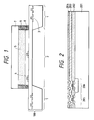
- Fig. 17 schematically illustrates the construction of a drive circuit for active matrix type liquid crystal display elements that has been conventionally used.
- reference numeral 301 denotes a picture element switch; 305, a liquid crystal picture element; 306, a transparent substrate; 302, a buffer portion; 303, a horizontal shift register; and 304, a vertical shift register.
- Luminance signals and sound signals of televisions are compressed in a certain band and are transferred to the buffer portion 302 that is driven by the horizontal shift register 303 having a driving capacity enough to be able to follow up the frequencies of the band.
- the signals are transferred to the liquid crystal in the period in which the picture element switch 301 is kept "ON" by the vertical shift register 304.
- Performance required for each circuit should be considered here. Assume that, taking account of high-grade televisions, they operate at a frame frequency of 60 Hz, a scanning line number of about 1,000 lines, a horizontal scanning period of about 30 ⁇ sec (effective scanning period: 27 ⁇ sec) and a horizontal picture element number of abut 1,500 elements, the television signals are transferred to the buffer at a frequency of about 45 MHz. Hence, each circuit is required to have the following performance:
- V m represents a voltage that gives a maximum or minimum transmittance of a liquid crystal
- V t represents a liquid-crystal threshold voltage obtained from a V-T (voltage-transmittance) curve.
- the picture element switch and the vertical shift register may have a relatively small driving capacity, but the horizontal shift register and the buffer portion are required to drive at a high speed.
- measures are taken such that the picture element switch and the vertical shift register are formed in a monolithic fashion together with liquid crystals, using polycrystalline silicon or amorphous silicon thin-film transistors (TFTs) deposited on a glass substrate; in other peripheral circuits, IC chips are externally packaged.
- TFTs polycrystalline silicon or amorphous silicon thin-film transistors
- transistors must be made larger in size or circuits must be complicatedly designed, because of a small driving capacity of individual TFTs.
- liquid crystal imaging apparatus such as VTR camera viewfinders or projection display devices, it is important for the substrate to be light-transmissive in their visible light regions.
- peripheral drive circuits with high-performance liquid crystal picture elements are required in order to accomplish high-performance liquid crystal display devices, and a semiconductor layer on which semiconductor elements constituting them are formed should be formed of a semiconductor monocrystalline layer having a good crystallinity.
- Such peripheral drive circuits must be screened from light.
- the active matrix element which orients a liquid crystal in accordance with a signal, it need not necessarily be formed by monocrystalline transistors, but transistors must be formed on a light-transmitting film.
- peripheral drive circuit element and the active matrix element are built in separate substrates, it becomes necessary to connect the both by wire bonding or the like, which results in a complicated process. Thus, it has been sought to make an improvement so that a cost decrease can be achieved and picture elements can be made much finer.
- An object of the present invention is to provide a semiconductor device and a liquid crystal display device that enable fabrication of an element required to have a performance comparable to that of a monocrystalline element and an element required to be formed on a light-transmitting substrate, on the same substrate by a simple process.
- the present invention provides a semiconductor device comprising; a substrate comprising a semiconductor monocrystalline substrate on one principal surface side of which a light-transmitting film is formed; the substrate being prepared by removing from the other principal surface side thereof a semiconductor monocrystalline region present right beneath the light-transmitting film; a non-monocrystalline semiconductor element formed on the light-transmitting film; and a monocrystalline semiconductor element formed in a semiconductor monocrystalline region remaining in the substrate; the non-monocrystalline semiconductor element and the monocrystalline semiconductor element being electrically connected.
- the present invention also provides a process for fabricating the semiconductor device described above.
- Fig. 1 is a diagrammatic cross section to illustrate an example of the liquid crystal display device of the present invention.
- Fig. 2 is a cross section to illustrate a fabrication step in an embodiment of the liquid crystal display device of the present invention.
- Fig. 3 is a cross section to illustrate a fabrication step in an embodiment of the liquid crystal display device of the present invention.
- Fig. 4 is a cross section to illustrate a fabrication step in an embodiment of the liquid crystal display device of the present invention.
- Fig. 5 is a cross section to illustrate a fabrication step in an embodiment of the liquid crystal display device of the present invention.
- Fig. 6 is a cross section to illustrate a fabrication step in an embodiment of the liquid crystal display device of the present invention.
- Fig. 7 is a cross section to illustrate a fabrication step in an embodiment of the liquid crystal display device of the present invention.
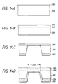
- Figs. 8A and 8B are diagrammatic cross sections to illustrate a construction and fabrication steps of a light transmission type semiconductor device according to the present invention.
- Figs. 9A and 9B are diagrammatic cross sections to illustrate a construction and fabrication steps of a light transmission type semiconductor device according to the present invention.
- Figs. 10A and 10B are diagrammatic cross sections to illustrate a construction and fabrication steps of a light transmission type semiconductor device according to the present invention.
- Fig. 11 is a graph to show a warpage of a substrate when films are multi-layered thereon.
- Fig. 12 is a diagrammatic illustration of an example of the liquid crystal display device according to the present invention.
- Fig. 13 is a diagrammatic cross section of a semiconductor substrate applicable in the semiconductor device of the present invention.
- Figs. 14A to 14D are diagrammatic cross sections of steps, to illustrate a fabrication process of a semiconductor substrate applicable in the semiconductor device of the present invention.
- Fig. 15 is a diagrammatic illustration of electrolytic etching.
- Fig. 16 is a diagrammatic cross section of a semiconductor substrate applicable in the semiconductor device of the present invention.
- Fig. 17 is a schematic illustration of the construction of a drive circuit for active matrix type liquid crystal display elements conventionally used.
- the semiconductor device of the present invention is constituted as described below. That is, the semiconductor device of the present invention is characterized by having; a substrate comprising a semiconductor monocrystalline substrate on one principal surface side of which a light-transmitting film is formed; the substrate being prepared by removing from the other side principal surface thereof a semiconductor monocrystalline region present right beneath the light-transmitting film; a non-monocrystalline semiconductor element formed on the light-transmitting film; and a monocrystalline semiconductor element formed in a semiconductor monocrystalline region remaining in the substrate; the non-monocrystalline semiconductor element and the monocrystalline semiconductor element being electrically connected.
- the liquid crystal display device of the present invention is characterized by having; a substrate comprising a semiconductor monocrystalline substrate on one principal surface side of which a light-transmitting film is formed; the substrate being prepared by removing from the other side principal surface thereof a semiconductor monocrystalline region present right beneath the light-transmitting film; an active matrix element formed on the light-transmitting film; and a drive circuit formed in a semiconductor monocrystalline region remaining in the substrate; the active matrix element and the drive circuit being electrically connected.
- the present invention also includes a process for fabricating the semiconductor device.
- the process for fabricating the semiconductor device comprises the steps of; forming an electric circuit on part of one principal surface of a semiconductor monocrystalline substrate, while forming an oxide film on another part of the principal surface and then forming a semiconductor element on the oxide film; wiring the electric circuit and the semiconductor element and electrically connecting them; forming an insulating film on the electric circuit and the semiconductor element; sealing a liquid crystal between a light-transmitting substrate different from the semiconductor monocrystalline substrate and the insulating film by the use of a sealing material; and etching the monocrystalline substrate to remove part thereof from its back surface of the one principal surface.
- the present invention employs a substrate comprised of a portion constituted of a light-transmitting film having light transmission properties and another portion constituted of a semiconductor monocrystalline region, which substrate comprises a semiconductor monocrystalline substrate on one principal surface side of which a light-transmitting film is formed and is prepared by removing from the other side principal surface thereof a semiconductor monocrystalline region present right beneath the light-transmitting film.
- the light-transmitting film on this substrate is provided with a semiconductor element as exemplified by a thin film transistor not required to have a performance comparable to that of a monocrystal, and the semiconductor monocrystalline region of the substrate is provided with a monocrystalline semiconductor element. This makes it possible to integrally form on the same substrate the semiconductor element (not required to have a performance comparable to that of a monocrystal) that must be formed on a light-transmitting substrate and the semiconductor element required to have a high performance.
- the semiconductor element that must be formed on a light-transmitting substrate and the semiconductor element required to have a high performance can be integrally formed on the same substrate, and hence the respective semiconductor elements can be electrically connected without fabricating them on the respectively different substrates and wiring them through mechanical connection such as wire bonding (i.e, they can be connected by Al wiring according to conventional deposition techniques).
- the circuit required to have a high performance can be provided on the semiconductor monocrystalline substrate so as to be constituted of a monocrystalline element. Hence, there may occur no problems such that the device must be made larger in size when such circuit is constituted of a non-monocrystalline material and the circuit must be complicatedly designed (e.g., block-divided driving).
- the present invention can be preferably used in active matrix type liquid crystal display devices. More specifically, the active matrix type liquid crystal display devices are required to provide active matrix elements such as thin film diodes and thin film transistors on a light-transmitting substrate and to form drive circuits such as shift registers as monocrystalline elements.
- the present invention makes it possible to integrally form the active matrix elements and drive circuits on the same substrate and also to electrically connect them without wiring by mechanical connection such as wire bonding.
- the semiconductor device of the present invention can be preferably used for a liquid crystal display device having a liquid crystal element serving as an optical element, a photosenser having a photoelectric transducer serving as an optical element, and so forth.
- a liquid crystal display device having a liquid crystal element serving as an optical element
- a photosenser having a photoelectric transducer serving as an optical element
- it is characterized in the substrate on which a semiconductor element preferably usable in an optical element is formed.
- Fig. 1 is a diagrammatic cross section to illustrate an example of the liquid crystal display device which is an example of the semiconductor device of the present invention.
- a substrate 100 is provided thereon with a light non-transmitting area 1 and a light-transmitting area 2.
- the light non-transmitting area 1 is provided therein with at least one semiconductor element 3 containing a monocrystalline semiconductor layer as an active region.
- the light-transmitting area 2 is provided thereon with at least one semiconductor element 4 containing a non-monocrystalline semiconductor layer as an active region.
- an aligning film 8 is further provided on the light-transmitting area 2, and a cover glass 7 serving as an opposing substrate is provided thereon. The space formed between them is fill with a liquid crystal 5 and its periphery is sealed with a sealing member 6.
- the semiconductor element used here in the present invention three-terminal elements such as bipolar transistors and MOS transistors or two-terminal elements such as diodes are preferably used.
- the light non-transmitting area 1 may preferably be comprised of a monocrystalline semiconductor, and can be readily made light non-transmissive by controlling its thickness or providing a light screening layer.
- an insulating thin film is preferably used. Stated specifically, it is a single layer or multiple layer formed of silicon oxide or silicon nitride.
- the non-monocrystalline semiconductor used in the semiconductor element provided thereon may be those having a crystal structure such as a polycrystalline, microcrystalline or amorphous structure. These can be readily formed as thin films by chemical vapor deposition (CVD), physical vapor deposition (PVD) or the like.
- the semiconductor element 4 may preferably be used as a picture element switch. As for the semiconductor element 3, it is used to constitute a peripheral drive circuit such as a drive circuit for driving the semiconductor element 4.
- the non-monocrystalline semiconductor layer may be made to serve as a photoelectric conversion portion or an active region of a switching transistor on the light-transmitting area 2.
- the substrate 100 used in the present invention it is preferable to use a substrate obtained by forming a light-transmitting insulating film on a substrate comprised of a monocrystalline semiconductor, and thereafter selectively removing the substrate at its portion to be made light-transmissive.
- the light-transmitting area is simultaneously formed when an element separating region for forming a semiconductor element in the light non-transmitting area is formed.
- a relatively thick oxide film is formed by selective oxidation.
- the wiring between elements can be carried out with ease by a conventional process.
- a silicon wafer 201 having a (100) plane on its principal surface is made ready.
- a peripheral drive circuit is formed in CMOS construction by a known technique, a monocrystalline wafer semiconductor process.
- a liquid crystal picture element display portion is covered with a field oxide film (serving as a light-transmitting film) 202.
- the field oxide film 202 is set in a thickness of 1 ⁇ m.
- polycrystalline silicon is used as gate materials, and they are each set in a thickness of 4,000 ⁇ .
- a source and a drain are formed in a self alignment fashion by ion implantation.
- As and BF2 are implanted at doses of 1 ⁇ 1016/cm2 and 2 ⁇ 1015/cm2, respectively.
- NSG (non-doped silicate glass) 203 is deposited by normal pressure CVD in a thickness of about 2,000 ⁇ .
- polycrystalline silicon 204 is deposited by low pressure CVD in a thickness of about 2,500 ⁇ .
- boron is ion-implanted at a dose of of 1 ⁇ 1011/cm2 over the whole surface (see Fig. 2).
- a resist pattern is left in the form of islands by photolithography.
- polycrystalline silicon regions 204 are formed at given positions by isotropic dry etching.
- an oxide film 207 of 500 ⁇ thick is made to grow on each polycrystalline silicon region 204 by pyrogenic oxidation at 950°C. These serve as gate oxide films of thin-film transistors (see Fig. 3).
- polycrystalline silicon is over again deposited by low pressure CVD, and gate electrodes 208 of the thin-film transistors are formed by anisotropic etching.
- the peripheral drive circuit portion is masked with a resist, and arsenic is ion-implanted at a dose of about 5 ⁇ 1015/cm2.
- heat treatment is applied in a nitrogen atmosphere at 900°C for 20 minutes to form the thin-film transistors (see Fig. 4.)
- NSG 209 is again deposited in a thickness of about 5,000 ⁇ by normal pressure CVD, and contact holes are made in the source and drain regions and gate electrode regions of the transistors.
- an electrode material such as aluminum is deposited by sputtering, and is worked into a given wiring form by dry etching to form wirings 210 (see Fig. 5).
- a capacitor portion is formed to cover the whole surface with a transparent insulating film 211.
- a sealing member 212 and a glass cover 214 are attached to seal a liquid crystal 213 (see Fig. 6).
- silicon is removed from the silicon substrate 201 so as to be hollowed out at its given area on the back surface.
- the wet etching solution does not dissolve silicon dioxide, and hence the etching stops at the field oxide film 202.
- the active matrix element area becomes transparent and comes to be functionable as a liquid crystal image display device (see Fig. 7).
- the above active matrix element makes use of an n-channel type MOSFET, and it may alternatively make use of a p-channel type MOSFET.
- the peripheral drive circuit constituted of a CMOS circuit in the above, may alternatively be constituted of a Bi-CMOS circuit containing a bipolar transistor, taking account of an improvement in driving capacity.
- the NSG film 203 shown in Fig. 2 is omitted, and the gate electrode portions of the n-MOS transistor 206 and p-MOS transistor 205 are beforehand thermally oxidized in a thickness of 300 ⁇ . At this time, none of impurities of the source and drain regions have been implanted in both the p-MOS transistor 206 and the p-MOS transistor 205. After the source/drain regions of the thin-film transistors have been formed, the peripheral drive circuit portion and the source/drain regions of the thin film transistors are simultaneously formed. The subsequent steps are the same as the fabrication steps described above.
- Whether or not the steps can be shortened in this way depends on whether or not the selectivity to silicon dioxide can be highly assured when the second polycrystalline silicon layers 204 are subjected to dry etching. This can be well accomplished by means of an existing dry etching apparatus making use of CF4.
- the semiconductor device of the present invention includes a device provided with a layer capable of controlling the stress on the whole multiple layers (a stress controlling layer), or provided with a layer capable of playing roles as the stress controlling layer and as an insulating layer used when a semiconductor integrated circuit is fabricated.
- the stress produced in the substrate when a non-transparent portion under the insulating layer is removed by etching acts as a tensile stress because of the multilayer film structure containing the stress controlling layer, and hence the multi-layer film where the semiconductor integrated circuit has been built in can be prevented from wrinkling.
- Figs, 8A and 8B are diagrammatic cross sections to illustrate a multi-layer film structure of a light transmission type semiconductor integrated circuit built in a monocrystalline silicon thin film on an insulating layer.
- Figs, 8A and 8B also illustrate fabrication steps of a semiconductor device for liquid crystal driving, where Fig. 8A shows a constitution in which the display area has not been made transparent, and Fig. 8B, a structure in which it has been made transparent by etching away the substrate 101.
- reference numeral 101 denotes an Si substrate; 102 and 103, SiO2 layers; and 110, an active region in which a liquid crystal driving MOS transistor is formed.
- the SiO2 layer 102 should preferably have a layer thickness of about 400 nm, and the SiO2 layer 103 should preferably have a layer thickness of about 1,100 nm.
- Reference numeral 104 denotes an LP-SiNx film (SiNx film formed by low-pressure gas phase synthesis) serving as the stress controlling layer according to the present Example; 105, an interlayer insulating film; 112, Al wiring; and 111, polysilicon gate wiring.
- Reference numeral 113 denotes a BPSG film provided to increase smoothness and insulating properties; 106 and 108, ITO films that hold between them a PSG film 107 or an SiNx film (a p-SiNx film) formed by plasma CVD, to form a liquid crystal holding capacitor.
- Reference numeral 109 denotes a passivation film, formed of p-SiNx, PSG, polyimide or the like.
- the LP-SiNx film 104 serves as the stress controlling layer of the whole multi-layer film where the semiconductor integrated circuit has been built in. It should preferably have a film thickness of about 600 nm.
- Each film was formed by using known techniques for fabricating semiconductor integrated circuits.
- the silicon substrate was covered with a base-resistant rubber except its portion right beneath the liquid crystal image display area, and the silicon substrate 101 was partially removed until the insulating film 102 was laid bare, using a tetramethylammonium hydroxdie (TMAH) solution.
- TMAH tetramethylammonium hydroxdie
- Fig. 12 illustrates the liquid crystal image display device according to the present Example, thus produced.
- reference numeral 101 denotes a silicon substrate; 501, a liquid crystal driving element layer; 502, a transparent resin; 503, an adhesive; 504, a liquid crystal; and 505, a cover glass.
- Fig. 11 is a graph to show how the stress changes as the respective layers of the multi-layer film having been made transparent in the above constitution are formed layer by layer, where the stress is shown by calculating it as a warpage of the wafer.
- the LP-SiNx film 104 is seen to have converted the stress of the whole multi-layer film into tensile stress, showing that the LP-SiNx film 104 as the stress controlling layer according to the present invention effectively acts.
- Table 2 also shows the stress produced in the multi-layer film when the layer thickness of the LP-SiNx film 104 was changed to range from 0 to 800 nm, where the stress is shown by calculating it as a warpage of the wafer.
- the stress of the whole multi-layer film calculated as a warpage of the wafer, was in a tensile stress of from 0 to 100 ⁇ m
- the removal of the silicon substrate 101 up to the bottom of the SiO2 layer 102 by etching made the semiconductor integrated circuit area on the upper part of the SiO2 film 102 transparent and then brought about the achievement of a uniform plane usable as that of a liquid crystal display device.
- Figs. 9A and 9B illustrate another example of the semiconductor device for liquid crystal driving of the present invention, where Fig. 9A shows a constitution in which the display area has not been made transparent, and Fig. 9B, a structure in which it has been made transparent by etching away the substrate 101.
- reference numeral 101 a silicon substrate; and 202, an LP-SiNx film.
- the LP-SiNx layer 202 serves as the stress controlling layer of the whole multi-layer film where a semiconductor integrated circuit has been built in. It should preferably have a layer thickness of from about 200 to about 400 nm.
- An SiO2 layer 203 may be provided so that the active layer can be made stable.
- Reference numeral 103 denotes an SiO2 layer.
- the SiO2 layer should preferably have a layer thickness of about 1,100 nm.
- Reference numeral 110 denotes an active region in which an MOS transistor for liquid crystal driving is formed.
- Reference numeral 204 denotes an interlayer insulating film for Al wiring 112 and polysilicon gate wiring 111.
- Reference numeral 203 denotes a BPSG film provideded to increase smoothness and insulating properties.
- ITO films denoted by reference numerals 106 and 108 hold between them a PSG film 107 or a p-SiNx film to form a liquid crystal holding capacitor.
- Reference numeral 109 denotes a passivation film, formed of p-SiNx, PSG, polyimide or the like.
- Each film was formed by using known techniques for fabricating semiconductor integrated circuits.
- the silicon substrate was covered with a base-resistant rubber except its portion right beneath the liquid crystal image display area, and the silicon substrate 101 was partially removed until the insulating film 102 was laid bare, using a tetramethylammonium hydroxdie (TMAH) solution.
- TMAH tetramethylammonium hydroxdie
- the removal of the silicon substrate 101 up to the bottom of the LP-SiNx layer 202 by etching made the semiconductor integrated circuit area on the upper part of the LP-SiNx layer 202 transparent and then brought about the achievement of a uniform plane usable as that of a liquid crystal display device.
- Figs. 10A and 10B illustrate still another example of the semiconductor device for liquid crystal driving of the present invention, where Fig. 10A shows a constitution in which the display area has not been made transparent, and Fig. 10B, a structure in which it has been made transparent by etching away the substrate 101.
- reference numeral 101 denotes an Si substrate; 102 and 103, SiO2 layers; and 110, an active region in which a liquid crystal driving MOS transistor is formed.
- the layer 102 should preferably have a layer thickness of about 400 nm, and the layer 103 should preferably have a layer thickness of about 1,100 nm.
- Reference numeral 304 denotes an interlayer insulating film for Al wiring 112 and polysilicon gate wiring 111.
- the interlayer insulating film 304 serves as the stress controlling layer of the whole multi-layer film where a semiconductor integrated circuit has been built in.
- the interlayer insulating film 304 is comprised of a silicon oxide film formed by gas phase synthesis using TEOS as a starting material gas, and should preferably have a layer thickness of about 1 ⁇ m.
- ITO films denoted by reference numerals 106 and 108 hold between them a PSG film or p-SiNx film 107 to form a liquid crystal holding capacitor.
- Reference numeral 109 denotes a passivation film, formed of p-SiNx, PSG, polyimide or the like.
- Each film was formed by using known techniques for fabricating semiconductor integrated circuits.
- the silicon substrate was covered with a base-resistant rubber except its portion right beneath the liquid crystal image display area, and the silicon substrate 101 was partially removed until the insulating film 102 was laid bare, using a tetramethylammonium hydroxdie (TMAH) solution.
- TMAH tetramethylammonium hydroxdie
- the recess in the substrate formed by the partial removal was filled with a transparent resin to make the device transparent.
- the removal of the silicon substrate 101 up to the bottom of the SiO2 layer 102 by etching made the semiconductor integrated circuit area on the upper part of the SiO2 layer 102 transparent and then brought about the achievement of a uniform plane usable as that of a liquid crystal display device.
- a tensile-stressed film like the LP-SiNx film is provided in the multi-layer film so that the stress in the whole multilayer film can be controlled. This makes it possible to prevent the wrinkles or cracks due to internal stress from occurring even when the lower part silicon substrate is removed. As a result, a high-quality, light transmission type semiconductor device using monocrystals in the device can be accomplished.
- the semiconductor device of the present invention also includes a semiconductor device comprising a substrate comprised of a monocrystalline substrate on one principal surface side of which a diffusion layer having a conductivity type reverse to the conductivity type of the monocrystalline substrate is formed; the monocrystalline substrate being selectively removed on its side opposite to the principal surface.
- a substrate is shown in Fig. 13.
- reference numeral 101 denotes a silicon substrate; 102, a diffusion layer; and 103, a thermal oxide film serving as a mask material.
- a thin diffusion layer 102 supported on a relatively thick silicon substrate 101 is formed on a hollow groove.
- an insulating layer may be formed beneath the diffusion layer 102 at its part fronting the groove, whereby a semiconductor substrate of an SOI structure can be readily obtained.
- a p-type silicon monocrystalline substrate 201 with a specific resistance of from about 20 to 30 ⁇ cm was made ready. This substrate was oxided to a 500 ⁇ thickness (Fig. 14A).
- P+ is ion-implanted under conditions of 1 ⁇ 1011 to 1014 cm ⁇ 2/60 to 100 keV. Thereafter, heat treatment is applied at 1,000°C for 1 hour in an environment of N2 to form an n-type diffusion layer 203.
- the diffusion layer has a depth of about 5,000 ⁇ (Fig. 14B).
- an Si3N4 film 204 is formed as a mask material. Though variable depending on conditions for the etching of Si, a silicon wafer of 5 inch diameter and 625 ⁇ m thick can be well etched when the Si3N4 film is formed in a thickness of about 200 ⁇ , since, if KOH (80°C) is used, Si is etched at a rate of 12,000 ⁇ /min and Si3N4 film is etched at a rate of 0.5 ⁇ /min.
- the resulting substrate is further subjected to electrolytic etching.
- the electrolytic etching is conceptionally illustrated in Fig. 15.
- the substrate 201 is brought into contact with a metal electrode 304, and a positive voltage 302 is applied thereto.
- An opposing electrode 305 is formed using a platinum plate, and a negative voltage 303 is applied thereto.
- An etching solution (an etchant) 301 is an ethylenediamine-pyrocatechol-water mixed solution with a compositional ratio of 7.5 liter ethylenediamine, 1.2 kg pyrocatechol and 2.4 liter water. Temperature is set at 110°C and stirring is thoroughly carried out.
- This electrolytic etching has been developed by T.N. Jackson et al., and is disclosed in detail in IEEE Device Letters, Vol. EDL-2, No. 2 (1981, p.44). Besides the above etching solution, the etching can also be carried out using KOH, TMAH or the like.
- the etching actually stops at its joint surface to the diffusion layer 203.
- the etching proceeds at a rate of 15,000 ⁇ /min in the p-region and 5 ⁇ /min in the n-region, so that the selectivity ratio is about 3,000.
- the n-type diffusion layer (thin film) 203 remains only at the desired place (Fig. 14C).
- this thin-film diffusion layer 203 is oxidized, whereby this thin film is formed into an SOI substrate 206 (Fig. 14D).
- Example 5 a process for preparing the SOI substrate has been described. In the present Example, a method by which this substrate is made light-transmissive to the visible light region will be further described.
- Fig. 16 is a diagrammatic cross section to illustrate the present Example.
- reference numeral 401 denotes a silicon substrate; 402, a diffusion layer; 403, a mask material used when silicon is etched; 404, a thermal oxide layer; and 405, an insulating layer for reinforcing the thin film.
- the process for preparing the substrate of the present Example is the same as that in Example 5 up to the step described in relation to Fig. 14C.
- a step characteristic of the present Example will be described below in detail with reference to Fig. 16, in particular, the step of forming a transparent insulating film 405.
- An oxidation-resistant layer is formed on the layer 402.
- the film is removed by patterning at its part to be made light-transmissive. Subsequently, this is oxidized at a high temperature of 500°C or above, so that part of the semiconductor substrate is oxidized and light-transmitting insulating films 404 and 405 are formed.
- the SOI structure in which a semiconductor layer 406 is formed on a light-transmitting insulating film 405. This enables easy formation of a structure advantageous for the construction of photosemiconductor devices that require a light-transmitting portion such as liquid crystal display devices or the like.
- an MOS transistor for switching picture elements may be formed on the region 406 and a peripheral drive circuit such as a shift register may be formed in the region 407.
- a peripheral drive circuit such as a shift register
- silicone rubber, epoxy resin, SiN x , SiO x , or the like may be deposited so that the film strength of the region 406 can be improved.
- the present invention employs the substrate comprised of a portion constituted of a light-transmitting film having light transmission properties and another portion constituted of a semiconductor monocrystalline region, which substrate comprises a semiconductor monocrystalline substrate on one principal surface side of which a light-transmitting film is formed and is prepared by removing from the other side principal surface thereof a semiconductor monocrystalline region present right beneath the light-transmitting film.
- the light-transmitting film on this substrate is provided with a semiconductor element not required to have a performance comparable to that of a monocrystal, and the semiconductor monocrystalline region of the substrate is provided with a monocrystalline semiconductor element. This makes it possible to integrally form on the same substrate the semiconductor element (not required to have a performance comparable to that of a monocrystal) that must be formed on a light-transmitting substrate and the semiconductor element required to have a high performance.
- the semiconductor element that must be formed on a light-transmitting substrate and the semiconductor element required to have a high performance can be integrally formed on the same substrate, and hence the respective semiconductor elements can be electrically connected without fabricating them on the respectively different substrate and wiring them through mechanical connection such as wire bonding.
- the circuit required to have a high performance can be provided on the semiconductor monocrystalline substrate so as to be constituted of a monocrystalline element. Hence, there may occur no problems such that the device must be made larger in size when such circuit is constituted of a non-monocrystal and the circuit must be complicatedly designed (e.g., block-divided driving).
Landscapes
- Physics & Mathematics (AREA)
- Nonlinear Science (AREA)
- Mathematical Physics (AREA)
- Chemical & Material Sciences (AREA)
- Crystallography & Structural Chemistry (AREA)
- General Physics & Mathematics (AREA)
- Optics & Photonics (AREA)
- Engineering & Computer Science (AREA)
- Microelectronics & Electronic Packaging (AREA)
- Liquid Crystal (AREA)
- Thin Film Transistor (AREA)
Abstract
Description
- This invention relates to a semiconductor device, a semiconductor device applicable for a liquid crystal display device, and a process for fabricating the semiconductor device. More particularly, the present invention relates to a semiconductor device applicable for a liquid crystal display device, comprising a non-monocrystalline semiconductor element and a monocrystalline semiconductor element which are provided on the same substrate, and a process for fabricating such a semiconductor device.
- As prior art, semiconductor devices used for liquid crystal display devices will be first described.
- Liquid crystal display devices provided with active matrix elements have been hitherto made commercially available as flat panel display devices or projection televisions.
- Fig. 17 schematically illustrates the construction of a drive circuit for active matrix type liquid crystal display elements that has been conventionally used. In Fig. 17,
reference numeral 301 denotes a picture element switch; 305, a liquid crystal picture element; 306, a transparent substrate; 302, a buffer portion; 303, a horizontal shift register; and 304, a vertical shift register. Luminance signals and sound signals of televisions are compressed in a certain band and are transferred to thebuffer portion 302 that is driven by thehorizontal shift register 303 having a driving capacity enough to be able to follow up the frequencies of the band. Next, the signals are transferred to the liquid crystal in the period in which thepicture element switch 301 is kept "ON" by thevertical shift register 304. - Performance required for each circuit should be considered here. Assume that, taking account of high-grade televisions, they operate at a frame frequency of 60 Hz, a scanning line number of about 1,000 lines, a horizontal scanning period of about 30 µsec (effective scanning period: 27 µsec) and a horizontal picture element number of abut 1,500 elements, the television signals are transferred to the buffer at a frequency of about 45 MHz. Hence, each circuit is required to have the following performance:
- (1) The horizontal shift register can drive at 45 MHz or above (i.e., driving capacity);
- (2) the vertical shift register can drive at 500 kHz or above;
- (3) a transfer switch that is driven by the horizontal shift register and transfers television signals to the buffer can drive at 45 MHz or above; and
- (4) the picture element switch can drive at 500 kHz or above.
- What is meant by the driving capacity herein referred to is that, when a liquid crystal picture element is made to have a certain gradation number N, a voltage not lower than the following voltage is transferred within the above period.

wherein Vm represents a voltage that gives a maximum or minimum transmittance of a liquid crystal, and Vt represents a liquid-crystal threshold voltage obtained from a V-T (voltage-transmittance) curve. - As is seen from these, the picture element switch and the vertical shift register may have a relatively small driving capacity, but the horizontal shift register and the buffer portion are required to drive at a high speed. For this reason, in existing liquid crystal display devices, measures are taken such that the picture element switch and the vertical shift register are formed in a monolithic fashion together with liquid crystals, using polycrystalline silicon or amorphous silicon thin-film transistors (TFTs) deposited on a glass substrate; in other peripheral circuits, IC chips are externally packaged. Although it is attempted to form the peripheral circuits also in a monolithic fashion using polycrystalline silicon TFTs, transistors must be made larger in size or circuits must be complicatedly designed, because of a small driving capacity of individual TFTs. Meanwhile, as for liquid crystal imaging apparatus such as VTR camera viewfinders or projection display devices, it is important for the substrate to be light-transmissive in their visible light regions.
- As stated above, peripheral drive circuits with high-performance liquid crystal picture elements are required in order to accomplish high-performance liquid crystal display devices, and a semiconductor layer on which semiconductor elements constituting them are formed should be formed of a semiconductor monocrystalline layer having a good crystallinity. Such peripheral drive circuits must be screened from light.
- As for the active matrix element which orients a liquid crystal in accordance with a signal, it need not necessarily be formed by monocrystalline transistors, but transistors must be formed on a light-transmitting film.
- An example will be given below. Assume that the total load of the active matrix element is 50 fF and the voltage swing width for liquid crystal orientation is 10 V, a charge of;

must be flowed in a given time. When it is taken into account to drive this element at 500 kHz as stated above, the saturated current required for the transistors is;
and is;
Thus, it is seen to be enough for the saturated current to be 250 nA or more. This is a value that can be well achieved by the polycrystalline silicon or amorphous silicon thin-film transistors. - Items required in the peripheral drive circuit elements and the active matrix elements can be summarized as shown in Table 1.
Table 1 Peripheral drive circuit element Active matrix element Current driving capacity: Comparable to monocrystalline element Higher than polycrystalline or amorphous element Light transmission properties of substrate: Unnecessary Necessary - In instances in which both the driving capacity comparable to monocrystalline elements and the light transmission properties of substrates are required in elements, a monocrystalline SOI (silicon on insulator) must be used. In the case of liquid crystal display devices, however, there is no element in which both of the above two items of performance are required, and hence one may have an idea of a constitution in which the peripheral drive circuit element and the active matrix element are separately built in.
- If, however, the peripheral drive circuit element and the active matrix element are built in separate substrates, it becomes necessary to connect the both by wire bonding or the like, which results in a complicated process. Thus, it has been sought to make an improvement so that a cost decrease can be achieved and picture elements can be made much finer.
- An object of the present invention is to provide a semiconductor device and a liquid crystal display device that enable fabrication of an element required to have a performance comparable to that of a monocrystalline element and an element required to be formed on a light-transmitting substrate, on the same substrate by a simple process.
- To achieve the above object, the present invention provides a semiconductor device comprising;
a substrate comprising a semiconductor monocrystalline substrate on one principal surface side of which a light-transmitting film is formed; the substrate being prepared by removing from the other principal surface side thereof a semiconductor monocrystalline region present right beneath the light-transmitting film;
a non-monocrystalline semiconductor element formed on the light-transmitting film; and
a monocrystalline semiconductor element formed in a semiconductor monocrystalline region remaining in the substrate;
the non-monocrystalline semiconductor element and the monocrystalline semiconductor element being electrically connected. - The present invention also provides a process for fabricating the semiconductor device described above.
- Fig. 1 is a diagrammatic cross section to illustrate an example of the liquid crystal display device of the present invention.
- Fig. 2 is a cross section to illustrate a fabrication step in an embodiment of the liquid crystal display device of the present invention.
- Fig. 3 is a cross section to illustrate a fabrication step in an embodiment of the liquid crystal display device of the present invention.
- Fig. 4 is a cross section to illustrate a fabrication step in an embodiment of the liquid crystal display device of the present invention.
- Fig. 5 is a cross section to illustrate a fabrication step in an embodiment of the liquid crystal display device of the present invention.
- Fig. 6 is a cross section to illustrate a fabrication step in an embodiment of the liquid crystal display device of the present invention.
- Fig. 7 is a cross section to illustrate a fabrication step in an embodiment of the liquid crystal display device of the present invention.
- Figs. 8A and 8B are diagrammatic cross sections to illustrate a construction and fabrication steps of a light transmission type semiconductor device according to the present invention.
- Figs. 9A and 9B are diagrammatic cross sections to illustrate a construction and fabrication steps of a light transmission type semiconductor device according to the present invention.
- Figs. 10A and 10B are diagrammatic cross sections to illustrate a construction and fabrication steps of a light transmission type semiconductor device according to the present invention.
- Fig. 11 is a graph to show a warpage of a substrate when films are multi-layered thereon.
- Fig. 12 is a diagrammatic illustration of an example of the liquid crystal display device according to the present invention.
- Fig. 13 is a diagrammatic cross section of a semiconductor substrate applicable in the semiconductor device of the present invention.
- Figs. 14A to 14D are diagrammatic cross sections of steps, to illustrate a fabrication process of a semiconductor substrate applicable in the semiconductor device of the present invention.
- Fig. 15 is a diagrammatic illustration of electrolytic etching.
- Fig. 16 is a diagrammatic cross section of a semiconductor substrate applicable in the semiconductor device of the present invention.
- Fig. 17 is a schematic illustration of the construction of a drive circuit for active matrix type liquid crystal display elements conventionally used.
- The semiconductor device of the present invention is constituted as described below. That is, the semiconductor device of the present invention is characterized by having;
a substrate comprising a semiconductor monocrystalline substrate on one principal surface side of which a light-transmitting film is formed; the substrate being prepared by removing from the other side principal surface thereof a semiconductor monocrystalline region present right beneath the light-transmitting film;
a non-monocrystalline semiconductor element formed on the light-transmitting film; and
a monocrystalline semiconductor element formed in a semiconductor monocrystalline region remaining in the substrate;
the non-monocrystalline semiconductor element and the monocrystalline semiconductor element being electrically connected. - The liquid crystal display device of the present invention is characterized by having;
a substrate comprising a semiconductor monocrystalline substrate on one principal surface side of which a light-transmitting film is formed; the substrate being prepared by removing from the other side principal surface thereof a semiconductor monocrystalline region present right beneath the light-transmitting film;
an active matrix element formed on the light-transmitting film; and
a drive circuit formed in a semiconductor monocrystalline region remaining in the substrate;
the active matrix element and the drive circuit being electrically connected. - The present invention also includes a process for fabricating the semiconductor device.
- The process for fabricating the semiconductor device comprises the steps of;
forming an electric circuit on part of one principal surface of a semiconductor monocrystalline substrate, while forming an oxide film on another part of the principal surface and then forming a semiconductor element on the oxide film;
wiring the electric circuit and the semiconductor element and electrically connecting them;
forming an insulating film on the electric circuit and the semiconductor element;
sealing a liquid crystal between a light-transmitting substrate different from the semiconductor monocrystalline substrate and the insulating film by the use of a sealing material; and
etching the monocrystalline substrate to remove part thereof from its back surface of the one principal surface. - The present invention employs a substrate comprised of a portion constituted of a light-transmitting film having light transmission properties and another portion constituted of a semiconductor monocrystalline region, which substrate comprises a semiconductor monocrystalline substrate on one principal surface side of which a light-transmitting film is formed and is prepared by removing from the other side principal surface thereof a semiconductor monocrystalline region present right beneath the light-transmitting film. The light-transmitting film on this substrate is provided with a semiconductor element as exemplified by a thin film transistor not required to have a performance comparable to that of a monocrystal, and the semiconductor monocrystalline region of the substrate is provided with a monocrystalline semiconductor element. This makes it possible to integrally form on the same substrate the semiconductor element (not required to have a performance comparable to that of a monocrystal) that must be formed on a light-transmitting substrate and the semiconductor element required to have a high performance.
- According to the present invention, as described above, the semiconductor element that must be formed on a light-transmitting substrate and the semiconductor element required to have a high performance can be integrally formed on the same substrate, and hence the respective semiconductor elements can be electrically connected without fabricating them on the respectively different substrates and wiring them through mechanical connection such as wire bonding (i.e, they can be connected by Al wiring according to conventional deposition techniques).
- In the present invention, the circuit required to have a high performance can be provided on the semiconductor monocrystalline substrate so as to be constituted of a monocrystalline element. Hence, there may occur no problems such that the device must be made larger in size when such circuit is constituted of a non-monocrystalline material and the circuit must be complicatedly designed (e.g., block-divided driving).
- The present invention can be preferably used in active matrix type liquid crystal display devices. More specifically, the active matrix type liquid crystal display devices are required to provide active matrix elements such as thin film diodes and thin film transistors on a light-transmitting substrate and to form drive circuits such as shift registers as monocrystalline elements. However, employment of the present invention makes it possible to integrally form the active matrix elements and drive circuits on the same substrate and also to electrically connect them without wiring by mechanical connection such as wire bonding.
- The present invention will be described in detail by giving Examples with reference to the accompanying drawings.
- The semiconductor device of the present invention can be preferably used for a liquid crystal display device having a liquid crystal element serving as an optical element, a photosenser having a photoelectric transducer serving as an optical element, and so forth. In particular, it is characterized in the substrate on which a semiconductor element preferably usable in an optical element is formed.
- To make it easy to understand the present invention, the semiconductor device according to the present invention will be described below with reference to Fig. 1. Fig. 1 is a diagrammatic cross section to illustrate an example of the liquid crystal display device which is an example of the semiconductor device of the present invention.
- A
substrate 100 is provided thereon with a lightnon-transmitting area 1 and a light-transmittingarea 2. The lightnon-transmitting area 1 is provided therein with at least onesemiconductor element 3 containing a monocrystalline semiconductor layer as an active region. Meanwhile, the light-transmittingarea 2 is provided thereon with at least onesemiconductor element 4 containing a non-monocrystalline semiconductor layer as an active region. To set up a liquid crystal display device, an aligning film 8 is further provided on the light-transmittingarea 2, and acover glass 7 serving as an opposing substrate is provided thereon. The space formed between them is fill with aliquid crystal 5 and its periphery is sealed with a sealingmember 6. As the semiconductor element used here in the present invention, three-terminal elements such as bipolar transistors and MOS transistors or two-terminal elements such as diodes are preferably used. - The light
non-transmitting area 1 may preferably be comprised of a monocrystalline semiconductor, and can be readily made light non-transmissive by controlling its thickness or providing a light screening layer. - As for the light-transmitting
area 2, an insulating thin film is preferably used. Stated specifically, it is a single layer or multiple layer formed of silicon oxide or silicon nitride. The non-monocrystalline semiconductor used in the semiconductor element provided thereon may be those having a crystal structure such as a polycrystalline, microcrystalline or amorphous structure. These can be readily formed as thin films by chemical vapor deposition (CVD), physical vapor deposition (PVD) or the like. - The
semiconductor element 4 may preferably be used as a picture element switch. As for thesemiconductor element 3, it is used to constitute a peripheral drive circuit such as a drive circuit for driving thesemiconductor element 4. - Meanwhile, when the photoelectric transducer is used as an optical element, the non-monocrystalline semiconductor layer may be made to serve as a photoelectric conversion portion or an active region of a switching transistor on the light-transmitting
area 2. - As the
substrate 100 used in the present invention, it is preferable to use a substrate obtained by forming a light-transmitting insulating film on a substrate comprised of a monocrystalline semiconductor, and thereafter selectively removing the substrate at its portion to be made light-transmissive. - More preferably, the light-transmitting area is simultaneously formed when an element separating region for forming a semiconductor element in the light non-transmitting area is formed. Stated specifically, a relatively thick oxide film is formed by selective oxidation.
- Thus, because of substantial agreement in the level of the surfaces on the light
non-transmitting area 1 and light-transmittingarea 2, the wiring between elements can be carried out with ease by a conventional process. - A process for producing the above liquid crystal display device will be described below with reference to Figs. 2 to 7.
- First, a
silicon wafer 201 having a (100) plane on its principal surface is made ready. A peripheral drive circuit is formed in CMOS construction by a known technique, a monocrystalline wafer semiconductor process. At this time, a liquid crystal picture element display portion is covered with a field oxide film (serving as a light-transmitting film) 202. In the present Example, thefield oxide film 202 is set in a thickness of 1 µm. In both an n-MOS transistor 206 and a p-MOS transistor 205, polycrystalline silicon is used as gate materials, and they are each set in a thickness of 4,000 Å. A source and a drain are formed in a self alignment fashion by ion implantation. In the n-MOS transistor 206 and the p-MOS transistor 205, As and BF₂ are implanted at doses of 1 × 10¹⁶/cm² and 2 × 10¹⁵/cm², respectively. - After the impurity ions have been implanted in the source and drain portions, NSG (non-doped silicate glass) 203 is deposited by normal pressure CVD in a thickness of about 2,000 Å. Next,
polycrystalline silicon 204 is deposited by low pressure CVD in a thickness of about 2,500 Å. Then, boron is ion-implanted at a dose of of 1 × 10¹¹/cm² over the whole surface (see Fig. 2). - Next, on the portion where an active matrix element is to be formed, a resist pattern is left in the form of islands by photolithography. Using the resist as a mask,
polycrystalline silicon regions 204 are formed at given positions by isotropic dry etching. Thereafter, anoxide film 207 of 500 Å thick is made to grow on eachpolycrystalline silicon region 204 by pyrogenic oxidation at 950°C. These serve as gate oxide films of thin-film transistors (see Fig. 3). - Next, polycrystalline silicon is over again deposited by low pressure CVD, and
gate electrodes 208 of the thin-film transistors are formed by anisotropic etching. Thereafter, the peripheral drive circuit portion is masked with a resist, and arsenic is ion-implanted at a dose of about 5 × 10¹⁵/cm². Then, heat treatment is applied in a nitrogen atmosphere at 900°C for 20 minutes to form the thin-film transistors (see Fig. 4.) - Next,
NSG 209 is again deposited in a thickness of about 5,000 Å by normal pressure CVD, and contact holes are made in the source and drain regions and gate electrode regions of the transistors. - In that instance, because of a difference between the thickness 7,000 Å of the interlayer insulating films (203 and 209) in the peripheral drive circuit area (area I) and the thickness 5,000 Å of the
interlayer insulating film 209 in the active matrix element area (area II), it is safer from the viewpoint of a process to make contact holes separately in the area I and in the area II. In practice, however, CHF₃- C₂F₆ type dry etching caused no trouble at all even when all the contact holes were made together. - Thereafter, an electrode material such as aluminum is deposited by sputtering, and is worked into a given wiring form by dry etching to form wirings 210 (see Fig. 5).
- Next, using a transparent electrode material such as ITO known in the art, a capacitor portion is formed to cover the whole surface with a transparent
insulating film 211. Thereafter, a sealingmember 212 and aglass cover 214 are attached to seal a liquid crystal 213 (see Fig. 6). - Finally, using a wet etching solution comprising KOH or an organic alkali such as ethylenediamine, silicon is removed from the
silicon substrate 201 so as to be hollowed out at its given area on the back surface. In that instance, the wet etching solution does not dissolve silicon dioxide, and hence the etching stops at thefield oxide film 202. As a result, the active matrix element area becomes transparent and comes to be functionable as a liquid crystal image display device (see Fig. 7). - An embodiment according to the present invention has been described above in detail. A modification as shown below is also possible.
- That is, the above active matrix element makes use of an n-channel type MOSFET, and it may alternatively make use of a p-channel type MOSFET.
- The peripheral drive circuit, constituted of a CMOS circuit in the above, may alternatively be constituted of a Bi-CMOS circuit containing a bipolar transistor, taking account of an improvement in driving capacity.
- For the purpose of decreasing steps, the following fabrication process is also possible.
- The
NSG film 203 shown in Fig. 2 is omitted, and the gate electrode portions of the n-MOS transistor 206 and p-MOS transistor 205 are beforehand thermally oxidized in a thickness of 300 Å. At this time, none of impurities of the source and drain regions have been implanted in both the p-MOS transistor 206 and the p-MOS transistor 205. After the source/drain regions of the thin-film transistors have been formed, the peripheral drive circuit portion and the source/drain regions of the thin film transistors are simultaneously formed. The subsequent steps are the same as the fabrication steps described above. - Whether or not the steps can be shortened in this way depends on whether or not the selectivity to silicon dioxide can be highly assured when the second polycrystalline silicon layers 204 are subjected to dry etching. This can be well accomplished by means of an existing dry etching apparatus making use of CF₄.
- In order to prevent wrinkles from occurring on a thin-film portion remaining after etching, and taking account of film thickness of films formed layer by layer and a stress produced when a single layer is formed, the semiconductor device of the present invention includes a device provided with a layer capable of controlling the stress on the whole multiple layers (a stress controlling layer), or provided with a layer capable of playing roles as the stress controlling layer and as an insulating layer used when a semiconductor integrated circuit is fabricated.
- In the device thus constituted, the stress produced in the substrate when a non-transparent portion under the insulating layer is removed by etching acts as a tensile stress because of the multilayer film structure containing the stress controlling layer, and hence the multi-layer film where the semiconductor integrated circuit has been built in can be prevented from wrinkling.
- An example thereof will be described with reference to Figs. 8A and 8B.
- Figs, 8A and 8B are diagrammatic cross sections to illustrate a multi-layer film structure of a light transmission type semiconductor integrated circuit built in a monocrystalline silicon thin film on an insulating layer. Figs, 8A and 8B also illustrate fabrication steps of a semiconductor device for liquid crystal driving, where Fig. 8A shows a constitution in which the display area has not been made transparent, and Fig. 8B, a structure in which it has been made transparent by etching away the
substrate 101. - In the drawings,
reference numeral 101 denotes an Si substrate; 102 and 103, SiO₂ layers; and 110, an active region in which a liquid crystal driving MOS transistor is formed. TheSiO₂ layer 102 should preferably have a layer thickness of about 400 nm, and theSiO₂ layer 103 should preferably have a layer thickness of about 1,100 nm.Reference numeral 104 denotes an LP-SiNx film (SiNx film formed by low-pressure gas phase synthesis) serving as the stress controlling layer according to the present Example; 105, an interlayer insulating film; 112, Al wiring; and 111, polysilicon gate wiring.Reference numeral 113 denotes a BPSG film provided to increase smoothness and insulating properties; 106 and 108, ITO films that hold between them aPSG film 107 or an SiNx film (a p-SiNx film) formed by plasma CVD, to form a liquid crystal holding capacitor.Reference numeral 109 denotes a passivation film, formed of p-SiNx, PSG, polyimide or the like. - In the present Example, the LP-
SiNx film 104 serves as the stress controlling layer of the whole multi-layer film where the semiconductor integrated circuit has been built in. It should preferably have a film thickness of about 600 nm. - Each film was formed by using known techniques for fabricating semiconductor integrated circuits.
- Next, after a black matrix and a color filter were formed on a cover glass, common electrodes were formed, followed by orientation treatment. The substrate on which the semiconductor integrated circuit had been formed was subjected to orientation, and a sealing material was printed. Thereafter, the cover glass and the substrate on which the semiconductor integrated circuit had been formed were put together and liquid crystal was injected into the space between them. To the steps concerning this liquid crystal, known techniques for producing liquid crystal display devices were applied.
- Thereafter, the silicon substrate was covered with a base-resistant rubber except its portion right beneath the liquid crystal image display area, and the
silicon substrate 101 was partially removed until the insulatingfilm 102 was laid bare, using a tetramethylammonium hydroxdie (TMAH) solution. In order to improve reliability, the recess in the substrate formed by the partial removal was filled with a transparent resin to make the device light-transmissive. Thus, a projection type liquid crystal image display device was completed. - Fig. 12 illustrates the liquid crystal image display device according to the present Example, thus produced. In the drawing,
reference numeral 101 denotes a silicon substrate; 501, a liquid crystal driving element layer; 502, a transparent resin; 503, an adhesive; 504, a liquid crystal; and 505, a cover glass. - Fig. 11 is a graph to show how the stress changes as the respective layers of the multi-layer film having been made transparent in the above constitution are formed layer by layer, where the stress is shown by calculating it as a warpage of the wafer.
- Most films formed in multiple layers are films with compressive stress that cause wrinkles. However, the LP-
SiNx film 104 is seen to have converted the stress of the whole multi-layer film into tensile stress, showing that the LP-SiNx film 104 as the stress controlling layer according to the present invention effectively acts. - Table 2 also shows the stress produced in the multi-layer film when the layer thickness of the LP-
SiNx film 104 was changed to range from 0 to 800 nm, where the stress is shown by calculating it as a warpage of the wafer. When the stress of the whole multi-layer film, calculated as a warpage of the wafer, was in a tensile stress of from 0 to 100 µm, the removal of thesilicon substrate 101 up to the bottom of theSiO₂ layer 102 by etching made the semiconductor integrated circuit area on the upper part of theSiO₂ film 102 transparent and then brought about the achievement of a uniform plane usable as that of a liquid crystal display device. When, however, the stress of the whole multi-layer film was on the side of compressive stress, the film became wrinkled, or when the stress of the whole multi-layer film, calculated as a warpage of the wafer, was in a tensile stress of more than 100 µm, the film cracked because of an excessive tensile stress.Table 2 Relationship between a warpage of 5''-Si (100) wafer and the state of the film Thickness of LP- SiNx film 104Warpage (µm) Direction of stress State of the film 0 nm +10 µm Compressive Wrinkled 100 nm 0 µm - Tensed 400 nm -30 µm Tensile Tensed 600 nm -100 µm Tensile Tensed 800 nm < -100 µm Tensile Broken - Figs. 9A and 9B illustrate another example of the semiconductor device for liquid crystal driving of the present invention, where Fig. 9A shows a constitution in which the display area has not been made transparent, and Fig. 9B, a structure in which it has been made transparent by etching away the
substrate 101. - In the drawings, reference numeral 101 a silicon substrate; and 202, an LP-SiNx film.
- In the present Example, the LP-
SiNx layer 202 serves as the stress controlling layer of the whole multi-layer film where a semiconductor integrated circuit has been built in. It should preferably have a layer thickness of from about 200 to about 400 nm. AnSiO₂ layer 203 may be provided so that the active layer can be made stable. -
Reference numeral 103 denotes an SiO₂ layer. The SiO₂ layer should preferably have a layer thickness of about 1,100 nm.Reference numeral 110 denotes an active region in which an MOS transistor for liquid crystal driving is formed.Reference numeral 204 denotes an interlayer insulating film forAl wiring 112 andpolysilicon gate wiring 111.Reference numeral 203 denotes a BPSG film provideded to increase smoothness and insulating properties. ITO films denoted byreference numerals PSG film 107 or a p-SiNx film to form a liquid crystal holding capacitor.Reference numeral 109 denotes a passivation film, formed of p-SiNx, PSG, polyimide or the like. - Each film was formed by using known techniques for fabricating semiconductor integrated circuits.
- Next, after a black matrix and a color filter were formed on a cover glass, common electrodes were formed, followed by orientation. The substrate on which the semiconductor integrated circuit had been formed was subjected to orientation, and a sealing material was printed. Thereafter, the both were put together and liquid crystal was injected into the space between them. To the steps concerning this liquid crystal, known techniques for producing liquid crystal display devices were applied.
- Thereafter, the silicon substrate was covered with a base-resistant rubber except its portion right beneath the liquid crystal image display area, and the
silicon substrate 101 was partially removed until the insulatingfilm 102 was laid bare, using a tetramethylammonium hydroxdie (TMAH) solution. In order to improve reliability, the recess in the substrate formed by the partial removal was filled with a transparent resin to make the device light-transmissive. Thus, a projection type liquid crystal image display device was completed. - When the stress of the whole multi-layer film, calculated as a warpage of the wafer, was in a tensile stress of from 0 to 100 µm, the removal of the
silicon substrate 101 up to the bottom of the LP-SiNx layer 202 by etching made the semiconductor integrated circuit area on the upper part of the LP-SiNx layer 202 transparent and then brought about the achievement of a uniform plane usable as that of a liquid crystal display device. When, however, the stress of the whole multi-layer film was on the side of compressive stress, the film became wrinkled, or when the stress of the whole multi-layer film, calculated as a warpage of the wafer, was in a tensile stress of more than 100 µm, the film cracked because of an excessive tensile stress. - Figs. 10A and 10B illustrate still another example of the semiconductor device for liquid crystal driving of the present invention, where Fig. 10A shows a constitution in which the display area has not been made transparent, and Fig. 10B, a structure in which it has been made transparent by etching away the
substrate 101. - In the drawings,
reference numeral 101 denotes an Si substrate; 102 and 103, SiO₂ layers; and 110, an active region in which a liquid crystal driving MOS transistor is formed. Thelayer 102 should preferably have a layer thickness of about 400 nm, and thelayer 103 should preferably have a layer thickness of about 1,100 nm.Reference numeral 304 denotes an interlayer insulating film forAl wiring 112 andpolysilicon gate wiring 111. - In the present Example, the
interlayer insulating film 304 serves as the stress controlling layer of the whole multi-layer film where a semiconductor integrated circuit has been built in. Theinterlayer insulating film 304 is comprised of a silicon oxide film formed by gas phase synthesis using TEOS as a starting material gas, and should preferably have a layer thickness of about 1 µm. - ITO films denoted by
reference numerals SiNx film 107 to form a liquid crystal holding capacitor.Reference numeral 109 denotes a passivation film, formed of p-SiNx, PSG, polyimide or the like. - Each film was formed by using known techniques for fabricating semiconductor integrated circuits.
- Next, after a black matrix and a color filter were formed on a cover glass, common electrodes were formed, followed by orientation. The substrate on which the semiconductor integrated circuit had been formed was subjected to orientation, and a sealing material was printed. Thereafter, the both were put together and liquid crystal was injected into the space between them. To the steps concerning this liquid crystal, known techniques for producing liquid crystal display devices were applied.
- Thereafter, the silicon substrate was covered with a base-resistant rubber except its portion right beneath the liquid crystal image display area, and the
silicon substrate 101 was partially removed until the insulatingfilm 102 was laid bare, using a tetramethylammonium hydroxdie (TMAH) solution. In order to improve reliability, the recess in the substrate formed by the partial removal was filled with a transparent resin to make the device transparent. Thus, a light-transmitting, projection type liquid crystal display device was completed. - When the stress of the whole multi-layer film, calculated as a warpage of the wafer, was in a tensile stress of from 0 to 100 µm, the removal of the
silicon substrate 101 up to the bottom of theSiO₂ layer 102 by etching made the semiconductor integrated circuit area on the upper part of theSiO₂ layer 102 transparent and then brought about the achievement of a uniform plane usable as that of a liquid crystal display device. - When, however, the stress of the whole multilayer film was on the side of compressive stress, the film became wrinkled, or when the stress of the whole multi-layer film, calculated as a warpage of the wafer, was in a tensile stress of more than 100 µm, the film cracked because of an excessive tensile stress.
- As shown in the above Examples, a tensile-stressed film like the LP-SiNx film is provided in the multi-layer film so that the stress in the whole multilayer film can be controlled. This makes it possible to prevent the wrinkles or cracks due to internal stress from occurring even when the lower part silicon substrate is removed. As a result, a high-quality, light transmission type semiconductor device using monocrystals in the device can be accomplished.
- The semiconductor device of the present invention also includes a semiconductor device comprising a substrate comprised of a monocrystalline substrate on one principal surface side of which a diffusion layer having a conductivity type reverse to the conductivity type of the monocrystalline substrate is formed; the monocrystalline substrate being selectively removed on its side opposite to the principal surface. Such a substrate is shown in Fig. 13.
- In Fig. 13,
reference numeral 101 denotes a silicon substrate; 102, a diffusion layer; and 103, a thermal oxide film serving as a mask material. In this example, athin diffusion layer 102 supported on a relativelythick silicon substrate 101 is formed on a hollow groove. Not shown in Fig. 13, an insulating layer may be formed beneath thediffusion layer 102 at its part fronting the groove, whereby a semiconductor substrate of an SOI structure can be readily obtained. - A process for preparing such an SOI substrate will be described in Example 5.
- A p-type
silicon monocrystalline substrate 201 with a specific resistance of from about 20 to 30 Ω·cm was made ready. This substrate was oxided to a 500 Å thickness (Fig. 14A). - Next, P⁺ is ion-implanted under conditions of 1 × 10¹¹ to 10¹⁴ cm⁻²/60 to 100 keV. Thereafter, heat treatment is applied at 1,000°C for 1 hour in an environment of N₂ to form an n-
type diffusion layer 203. The diffusion layer has a depth of about 5,000 Å (Fig. 14B). - Next, an
Si₃N₄ film 204 is formed as a mask material. Though variable depending on conditions for the etching of Si, a silicon wafer of 5 inch diameter and 625 µm thick can be well etched when the Si₃N₄ film is formed in a thickness of about 200 Å, since, if KOH (80°C) is used, Si is etched at a rate of 12,000 Å/min and Si₃N₄ film is etched at a rate of 0.5 Å/min. - Next, a resist mask is applied and the
Si₃N₄ film 204 at its desired place and theSiO₂ film 202 are etched away. - The resulting substrate is further subjected to electrolytic etching. The electrolytic etching is conceptionally illustrated in Fig. 15.
- First, the
substrate 201 is brought into contact with ametal electrode 304, and apositive voltage 302 is applied thereto. An opposingelectrode 305 is formed using a platinum plate, and anegative voltage 303 is applied thereto. An etching solution (an etchant) 301 is an ethylenediamine-pyrocatechol-water mixed solution with a compositional ratio of 7.5 liter ethylenediamine, 1.2 kg pyrocatechol and 2.4 liter water. Temperature is set at 110°C and stirring is thoroughly carried out. - This electrolytic etching has been developed by T.N. Jackson et al., and is disclosed in detail in IEEE Device Letters, Vol. EDL-2, No. 2 (1981, p.44). Besides the above etching solution, the etching can also be carried out using KOH, TMAH or the like.
- In this electrolytic etching, because of a large selectivity ratio between the
substrate 201 and thediffusion layer 203, the etching actually stops at its joint surface to thediffusion layer 203. The etching proceeds at a rate of 15,000 Å/min in the p-region and 5 Å/min in the n-region, so that the selectivity ratio is about 3,000. - Finally, as a result of the electrolytic etching, the n-type diffusion layer (thin film) 203 remains only at the desired place (Fig. 14C).
- If the polarity of the electrolytic etching is reversed, it is also possible to leave a p-type diffusion layer.
- Thereafter, this thin-
film diffusion layer 203 is oxidized, whereby this thin film is formed into an SOI substrate 206 (Fig. 14D). - In Example 5, a process for preparing the SOI substrate has been described. In the present Example, a method by which this substrate is made light-transmissive to the visible light region will be further described.
- Fig. 16 is a diagrammatic cross section to illustrate the present Example.
- In Fig. 16,
reference numeral 401 denotes a silicon substrate; 402, a diffusion layer; 403, a mask material used when silicon is etched; 404, a thermal oxide layer; and 405, an insulating layer for reinforcing the thin film. - The process for preparing the substrate of the present Example is the same as that in Example 5 up to the step described in relation to Fig. 14C. A step characteristic of the present Example will be described below in detail with reference to Fig. 16, in particular, the step of forming a transparent
insulating film 405. - An oxidation-resistant layer is formed on the
layer 402. The film is removed by patterning at its part to be made light-transmissive. Subsequently, this is oxidized at a high temperature of 500°C or above, so that part of the semiconductor substrate is oxidized and light-transmittinginsulating films - The constitution taken in this way makes it possible to form an SOI device in a
diffusion layer region 406 not subjected to oxidation and to form a usual device in adiffusion layer region 407. - It is also possible to obtain, as previously described, the SOI structure in which a
semiconductor layer 406 is formed on a light-transmittinginsulating film 405. This enables easy formation of a structure advantageous for the construction of photosemiconductor devices that require a light-transmitting portion such as liquid crystal display devices or the like. - When, for example, this is applied for a liquid crystal display device, an MOS transistor for switching picture elements may be formed on the
region 406 and a peripheral drive circuit such as a shift register may be formed in theregion 407. Thus, a device capable of high-speed drive can be readily obtained. - At the groove formed by applying the electrolytic etching, silicone rubber, epoxy resin, SiNx, SiOx, or the like may be deposited so that the film strength of the
region 406 can be improved. - As described above, the present invention employs the substrate comprised of a portion constituted of a light-transmitting film having light transmission properties and another portion constituted of a semiconductor monocrystalline region, which substrate comprises a semiconductor monocrystalline substrate on one principal surface side of which a light-transmitting film is formed and is prepared by removing from the other side principal surface thereof a semiconductor monocrystalline region present right beneath the light-transmitting film. The light-transmitting film on this substrate is provided with a semiconductor element not required to have a performance comparable to that of a monocrystal, and the semiconductor monocrystalline region of the substrate is provided with a monocrystalline semiconductor element. This makes it possible to integrally form on the same substrate the semiconductor element (not required to have a performance comparable to that of a monocrystal) that must be formed on a light-transmitting substrate and the semiconductor element required to have a high performance.
- In the present invention, the semiconductor element that must be formed on a light-transmitting substrate and the semiconductor element required to have a high performance can be integrally formed on the same substrate, and hence the respective semiconductor elements can be electrically connected without fabricating them on the respectively different substrate and wiring them through mechanical connection such as wire bonding.
- In the present invention, the circuit required to have a high performance can be provided on the semiconductor monocrystalline substrate so as to be constituted of a monocrystalline element. Hence, there may occur no problems such that the device must be made larger in size when such circuit is constituted of a non-monocrystal and the circuit must be complicatedly designed (e.g., block-divided driving).
- Thus, it is possible to greatly decrease mounting cost and to provide a semiconductor device that can be more advantageous as the picture elements have a higher density.
Claims (13)
- A semiconductor device comprising;
a substrate comprising a semiconductor monocrystalline substrate on one principal surface side of which a light-transmitting film is formed; said substrate being prepared by removing from the other principal surface side thereof a semiconductor monocrystalline region present right beneath said light-transmitting film;
a non-monocrystalline semiconductor element formed on said light-transmitting film; and
a monocrystalline semiconductor element formed in a semiconductor monocrystalline region remaining in said substrate;
said non-monocrystalline semiconductor element and said monocrystalline semiconductor element being electrically connected. - The semiconductor device according to claim 1, wherein said non-monocrystalline semiconductor element comprises a semiconductor element formed of a polycrystalline silicon or an amorphous silicon.
- The semiconductor device according to claim 1, wherein said semiconductor monocrystalline substrate comprises a silicon monocrystalline substrate having a (100) plane on its principal surface.
- A liquid crystal display device comprising;
a substrate comprising a semiconductor monocrystalline substrate on one principal surface side of which a light-transmitting film is formed; said substrate being prepared by removing from the other side principal surface thereof a semiconductor monocrystalline region present right beneath said light-transmitting film;
an active matrix element formed on said light-transmitting film; and
a drive circuit formed in a semiconductor monocrystalline region remaining in said substrate;
said active matrix element and said drive circuit being electrically connected. - The liquid crystal display device according to claim 4, wherein said active matrix element comprises a thin film diode or thin film transistor formed of a polycrystalline silicon or an amorphous silicon.
- The liquid crystal display device according to claim 4, wherein said semiconductor monocrystalline substrate comprises a silicon monocrystalline substrate having a (100) plane on its principal surface.
- A process for fabricating a semiconductor device, comprising the steps of;
forming an electric circuit on part of one principal surface of a semiconductor monocrystalline substrate, while forming an oxide film on another part of said principal surface and then forming a semiconductor element on the oxide film;
wiring said electric circuit and said semiconductor element and electrically connecting them;
forming an insulating film on said electric circuit and said semiconductor element;
sealing a liquid crystal between a light-transmitting substrate different from said semiconductor monocrystalline substrate and said insulating film by the use of a sealing material; and
etching said monocrystalline substrate to remove part thereof from its back surface of said one principal surface. - The process for fabricating a semiconductor device according to claim 7, wherein said semiconductor device is a liquid crystal display device.
- The process for fabricating a semiconductor device according to claim 7, wherein said insulating film is comprised of a multi-layer film comprising a stress controlling layer capable of converting the internal stress of said substrate nto tensile stress.
- The process for fabricating a semiconductor device according to claim 9, wherein said stress controlling layer comprises an SiNx film formed by low-pressure gas phase synthesis.
- The process for fabricating a semiconductor device according to claim 9, wherein said stress controlling layer is deposited before the step of wiring.
- The process for fabricating a semiconductor device according to claim 9, wherein said stress controlling layer comprises a silicon oxide film formed by gas phase synthesis.
- A semiconductor device for driving and switching an array of optical elements, which device comprises:
a substrate (100) having a mono-crystalline semiconductor peripheral portion (1) and a thinner light transmissive central portion (2);
peripheral drive circuit elements (3) formed in the monocrystalline semiconductor peripheral portion (1) of said substrate (100); and
active matrix elements (4), formed in non-monocrystalline material (8) integral with said substrate (100) located over the central portion (2) of said substrate (100), which active matrix elements (4) are electrically connected to said peripheral drive circuit elements (3).
Applications Claiming Priority (9)
| Application Number | Priority Date | Filing Date | Title |
|---|---|---|---|
| JP35774692 | 1992-12-25 | ||
| JP35774692A JPH06196675A (en) | 1992-12-25 | 1992-12-25 | Method for forming semiconductor substrate and semiconductor device using the substrate |
| JP357746/92 | 1992-12-25 | ||
| JP31165/93 | 1993-01-28 | ||
| JP3116593A JPH06222391A (en) | 1993-01-28 | 1993-01-28 | Semiconductor device and liquid crystal display device |
| JP3116593 | 1993-01-28 | ||
| JP16001993A JPH06347830A (en) | 1993-06-07 | 1993-06-07 | Light transmission type semiconductor device and its production |
| JP16001993 | 1993-06-07 | ||
| JP160019/93 | 1993-06-07 |
Publications (3)
| Publication Number | Publication Date |
|---|---|
| EP0604231A1 true EP0604231A1 (en) | 1994-06-29 |
| EP0604231B1 EP0604231B1 (en) | 2000-10-11 |
| EP0604231B8 EP0604231B8 (en) | 2001-04-11 |
Family
ID=27287229
Family Applications (1)
| Application Number | Title | Priority Date | Filing Date |
|---|---|---|---|
| EP93310476A Expired - Lifetime EP0604231B8 (en) | 1992-12-25 | 1993-12-23 | Semiconductor device applicable for liquid crystal display device, and process for its fabrication |
Country Status (3)
| Country | Link |
|---|---|
| US (1) | US6128052A (en) |
| EP (1) | EP0604231B8 (en) |
| DE (1) | DE69329545T2 (en) |
Cited By (2)
| Publication number | Priority date | Publication date | Assignee | Title |
|---|---|---|---|---|
| EP0811869A1 (en) * | 1996-06-04 | 1997-12-10 | Canon Kabushiki Kaisha | Liquid crystal display device and process for production thereof |
| EP0772245A3 (en) * | 1995-11-01 | 1998-03-11 | Canon Kabushiki Kaisha | Field effect semiconductor device and liquid crystal display apparatus |
Families Citing this family (5)
| Publication number | Priority date | Publication date | Assignee | Title |
|---|---|---|---|---|
| US6288764B1 (en) * | 1996-06-25 | 2001-09-11 | Semiconductor Energy Laboratory Co., Ltd. | Display device or electronic device having liquid crystal display panel |
| US6346978B1 (en) * | 1999-07-13 | 2002-02-12 | Sharp Laboratories Of America, Inc. | SOI TFT array substrate for LCD projection display |
| JP4217434B2 (en) * | 2002-07-04 | 2009-02-04 | キヤノン株式会社 | Through-hole forming method and inkjet head using the same |
| US7508034B2 (en) * | 2002-09-25 | 2009-03-24 | Sharp Kabushiki Kaisha | Single-crystal silicon substrate, SOI substrate, semiconductor device, display device, and manufacturing method of semiconductor device |
| JP2008181109A (en) * | 2006-12-27 | 2008-08-07 | Semiconductor Energy Lab Co Ltd | Liquid crystal display device and electronic apparatus using the same |
Citations (3)
| Publication number | Priority date | Publication date | Assignee | Title |
|---|---|---|---|---|
| GB2204980A (en) * | 1987-05-22 | 1988-11-23 | Philips Electronic Associated | Active matrix addressed liquid crystal display devices |
| EP0474474A2 (en) * | 1990-09-05 | 1992-03-11 | Seiko Instruments Inc. | Semiconductor light valve device and process for fabricating the same |
| EP0530972A2 (en) * | 1991-08-02 | 1993-03-10 | Canon Kabushiki Kaisha | Liquid crystal image display unit |
Family Cites Families (8)
| Publication number | Priority date | Publication date | Assignee | Title |
|---|---|---|---|---|
| JPS63101829A (en) * | 1986-10-17 | 1988-05-06 | Nec Corp | Active matrix liquid crystal display device and its production |
| DE3856418T2 (en) * | 1987-03-04 | 2001-03-01 | Advanced Micro Devices, Inc. | Passivation layer for integrated circuit structure |
| US5343064A (en) * | 1988-03-18 | 1994-08-30 | Spangler Leland J | Fully integrated single-crystal silicon-on-insulator process, sensors and circuits |
| US5258325A (en) * | 1990-12-31 | 1993-11-02 | Kopin Corporation | Method for manufacturing a semiconductor device using a circuit transfer film |
| US5258320A (en) * | 1990-12-31 | 1993-11-02 | Kopin Corporation | Single crystal silicon arrayed devices for display panels |
| CA2061796C (en) * | 1991-03-28 | 2002-12-24 | Kalluri R. Sarma | High mobility integrated drivers for active matrix displays |
| JP3526058B2 (en) * | 1992-08-19 | 2004-05-10 | セイコーインスツルメンツ株式会社 | Semiconductor device for light valve |
| US5258323A (en) * | 1992-12-29 | 1993-11-02 | Honeywell Inc. | Single crystal silicon on quartz |
-
1993
- 1993-12-23 EP EP93310476A patent/EP0604231B8/en not_active Expired - Lifetime
- 1993-12-23 DE DE69329545T patent/DE69329545T2/en not_active Expired - Fee Related
-
1997
- 1997-05-05 US US08/851,269 patent/US6128052A/en not_active Expired - Fee Related
Patent Citations (3)
| Publication number | Priority date | Publication date | Assignee | Title |
|---|---|---|---|---|
| GB2204980A (en) * | 1987-05-22 | 1988-11-23 | Philips Electronic Associated | Active matrix addressed liquid crystal display devices |
| EP0474474A2 (en) * | 1990-09-05 | 1992-03-11 | Seiko Instruments Inc. | Semiconductor light valve device and process for fabricating the same |
| EP0530972A2 (en) * | 1991-08-02 | 1993-03-10 | Canon Kabushiki Kaisha | Liquid crystal image display unit |
Cited By (3)
| Publication number | Priority date | Publication date | Assignee | Title |
|---|---|---|---|---|
| EP0772245A3 (en) * | 1995-11-01 | 1998-03-11 | Canon Kabushiki Kaisha | Field effect semiconductor device and liquid crystal display apparatus |
| EP0811869A1 (en) * | 1996-06-04 | 1997-12-10 | Canon Kabushiki Kaisha | Liquid crystal display device and process for production thereof |
| US6271897B1 (en) | 1996-06-04 | 2001-08-07 | Canon Kabushiki Kaisha | Process of producing a semiconductor device |
Also Published As
| Publication number | Publication date |
|---|---|
| US6128052A (en) | 2000-10-03 |
| DE69329545T2 (en) | 2001-05-31 |
| EP0604231B8 (en) | 2001-04-11 |
| DE69329545D1 (en) | 2000-11-16 |
| EP0604231B1 (en) | 2000-10-11 |
Similar Documents
| Publication | Publication Date | Title |
|---|---|---|
| US5258325A (en) | Method for manufacturing a semiconductor device using a circuit transfer film | |
| US6187605B1 (en) | Method of forming a semiconductor device for a light valve | |
| US5827755A (en) | Liquid crystal image display unit and method for fabricating semiconductor optical member | |
| EP0626099A1 (en) | High density electronic circuit modules | |
| KR100275828B1 (en) | Single crystal silicon on quartz | |
| US6022751A (en) | Production of electronic device | |
| US6271897B1 (en) | Process of producing a semiconductor device | |
| WO1994017440A1 (en) | Reflective liquid crystal display including driver devices integrally formed in monocrystalline semiconductor layer and method of fabricating the display | |
| EP0558007B1 (en) | Electrical connection between a region of silicon and a film of oxide containing indium | |
| JP4060882B2 (en) | Manufacturing method of electronic device | |
| US6128052A (en) | Semiconductor device applicable for liquid crystal display device, and process for its fabrication | |
| JP2824818B2 (en) | Active matrix liquid crystal display | |
| US5633176A (en) | Method of producing a semiconductor device for a light valve | |
| JPH09293876A (en) | Semiconductor element substrate, manufacturing method thereof, and semiconductor device using the substrate | |
| JPH10293322A (en) | Liquid crystal display device and manufacturing method thereof | |
| US6954235B1 (en) | Silicon-on-sapphire display apparatus and method of fabricating same | |
| JP3192620B2 (en) | Electronic device manufacturing method | |
| JP3154100B2 (en) | Manufacturing method of liquid crystal image display device | |
| JPH05241200A (en) | Liquid crystal display | |
| JPH06347830A (en) | Light transmission type semiconductor device and its production | |
| JPH06214241A (en) | Liquid crystal display device | |
| JPH06222391A (en) | Semiconductor device and liquid crystal display device | |
| JP3098815B2 (en) | Liquid crystal display | |
| JPH09172180A (en) | Semiconductor device and liquid crystal display device | |
| JPH09293875A (en) | Semiconductor element substrate, manufacturing method thereof, and semiconductor device using the substrate |
Legal Events
| Date | Code | Title | Description |
|---|---|---|---|
| PUAI | Public reference made under article 153(3) epc to a published international application that has entered the european phase |
Free format text: ORIGINAL CODE: 0009012 |
|
| AK | Designated contracting states |
Kind code of ref document: A1 Designated state(s): DE FR GB IT NL |
|
| 17P | Request for examination filed |
Effective date: 19941111 |
|
| 17Q | First examination report despatched |
Effective date: 19961018 |
|
| GRAG | Despatch of communication of intention to grant |
Free format text: ORIGINAL CODE: EPIDOS AGRA |
|
| GRAG | Despatch of communication of intention to grant |
Free format text: ORIGINAL CODE: EPIDOS AGRA |
|
| GRAH | Despatch of communication of intention to grant a patent |
Free format text: ORIGINAL CODE: EPIDOS IGRA |
|
| RIC1 | Information provided on ipc code assigned before grant |
Free format text: 7G 02F 1/136 A |
|
| GRAH | Despatch of communication of intention to grant a patent |
Free format text: ORIGINAL CODE: EPIDOS IGRA |
|
| GRAH | Despatch of communication of intention to grant a patent |
Free format text: ORIGINAL CODE: EPIDOS IGRA |
|
| GRAA | (expected) grant |
Free format text: ORIGINAL CODE: 0009210 |
|
| AK | Designated contracting states |
Kind code of ref document: B1 Designated state(s): DE FR GB IT NL |
|
| PG25 | Lapsed in a contracting state [announced via postgrant information from national office to epo] |
Ref country code: NL Free format text: LAPSE BECAUSE OF FAILURE TO SUBMIT A TRANSLATION OF THE DESCRIPTION OR TO PAY THE FEE WITHIN THE PRESCRIBED TIME-LIMIT Effective date: 20001011 Ref country code: IT Free format text: LAPSE BECAUSE OF FAILURE TO SUBMIT A TRANSLATION OF THE DESCRIPTION OR TO PAY THE FEE WITHIN THE PRESCRIBED TIME-LIMIT;WARNING: LAPSES OF ITALIAN PATENTS WITH EFFECTIVE DATE BEFORE 2007 MAY HAVE OCCURRED AT ANY TIME BEFORE 2007. THE CORRECT EFFECTIVE DATE MAY BE DIFFERENT FROM THE ONE RECORDED. Effective date: 20001011 |
|
| REF | Corresponds to: |
Ref document number: 69329545 Country of ref document: DE Date of ref document: 20001116 |
|
| ET | Fr: translation filed | ||
| RIN2 | Information on inventor provided after grant (corrected) |
Free format text: ASABA, TETSUO, C/O CANON KABUSHIKI KAISHA * SAKAMOTO, MASARU, C/O CANON KABUSHIKI KAISHA * GENCHI, YUTAKA, C/O CANON KABUSHIKI KAISHA |
|
| NLV1 | Nl: lapsed or annulled due to failure to fulfill the requirements of art. 29p and 29m of the patents act | ||
| PLBE | No opposition filed within time limit |
Free format text: ORIGINAL CODE: 0009261 |
|
| STAA | Information on the status of an ep patent application or granted ep patent |
Free format text: STATUS: NO OPPOSITION FILED WITHIN TIME LIMIT |
|
| 26N | No opposition filed | ||
| REG | Reference to a national code |
Ref country code: GB Ref legal event code: IF02 |
|
| PGFP | Annual fee paid to national office [announced via postgrant information from national office to epo] |
Ref country code: GB Payment date: 20071228 Year of fee payment: 15 |
|
| PGFP | Annual fee paid to national office [announced via postgrant information from national office to epo] |
Ref country code: DE Payment date: 20071231 Year of fee payment: 15 |
|
| PGFP | Annual fee paid to national office [announced via postgrant information from national office to epo] |
Ref country code: FR Payment date: 20071220 Year of fee payment: 15 |
|
| GBPC | Gb: european patent ceased through non-payment of renewal fee |
Effective date: 20081223 |
|
| REG | Reference to a national code |
Ref country code: FR Ref legal event code: ST Effective date: 20090831 |
|
| PG25 | Lapsed in a contracting state [announced via postgrant information from national office to epo] |
Ref country code: DE Free format text: LAPSE BECAUSE OF NON-PAYMENT OF DUE FEES Effective date: 20090701 |
|
| PG25 | Lapsed in a contracting state [announced via postgrant information from national office to epo] |
Ref country code: GB Free format text: LAPSE BECAUSE OF NON-PAYMENT OF DUE FEES Effective date: 20081223 |
|
| PG25 | Lapsed in a contracting state [announced via postgrant information from national office to epo] |
Ref country code: FR Free format text: LAPSE BECAUSE OF NON-PAYMENT OF DUE FEES Effective date: 20081231 |