EP0603514A2 - Method for thinning a semiconductor wafer - Google Patents
Method for thinning a semiconductor wafer Download PDFInfo
- Publication number
- EP0603514A2 EP0603514A2 EP93117874A EP93117874A EP0603514A2 EP 0603514 A2 EP0603514 A2 EP 0603514A2 EP 93117874 A EP93117874 A EP 93117874A EP 93117874 A EP93117874 A EP 93117874A EP 0603514 A2 EP0603514 A2 EP 0603514A2
- Authority
- EP
- European Patent Office
- Prior art keywords
- semiconductor wafer
- major surface
- support film
- substrate
- thinning
- Prior art date
- Legal status (The legal status is an assumption and is not a legal conclusion. Google has not performed a legal analysis and makes no representation as to the accuracy of the status listed.)
- Withdrawn
Links
- 239000004065 semiconductor Substances 0.000 title claims abstract description 123
- 238000000034 method Methods 0.000 title claims abstract description 39
- 238000000227 grinding Methods 0.000 claims abstract description 19
- 239000000758 substrate Substances 0.000 claims description 18
- 239000000853 adhesive Substances 0.000 claims description 13
- 230000001070 adhesive effect Effects 0.000 claims description 13
- 238000005530 etching Methods 0.000 claims description 9
- XLYOFNOQVPJJNP-UHFFFAOYSA-N water Substances O XLYOFNOQVPJJNP-UHFFFAOYSA-N 0.000 claims description 5
- MHAJPDPJQMAIIY-UHFFFAOYSA-N Hydrogen peroxide Chemical compound OO MHAJPDPJQMAIIY-UHFFFAOYSA-N 0.000 claims description 4
- QAOWNCQODCNURD-UHFFFAOYSA-N Sulfuric acid Chemical compound OS(O)(=O)=O QAOWNCQODCNURD-UHFFFAOYSA-N 0.000 claims description 4
- 230000002093 peripheral effect Effects 0.000 claims description 4
- 238000005096 rolling process Methods 0.000 claims description 4
- 238000004140 cleaning Methods 0.000 claims description 3
- QGZKDVFQNNGYKY-UHFFFAOYSA-N Ammonia Chemical compound N QGZKDVFQNNGYKY-UHFFFAOYSA-N 0.000 claims description 2
- VHUUQVKOLVNVRT-UHFFFAOYSA-N Ammonium hydroxide Chemical compound [NH4+].[OH-] VHUUQVKOLVNVRT-UHFFFAOYSA-N 0.000 claims description 2
- 239000000908 ammonium hydroxide Substances 0.000 claims description 2
- 238000001035 drying Methods 0.000 claims description 2
- 229910052751 metal Inorganic materials 0.000 abstract description 11
- 239000002184 metal Substances 0.000 abstract description 11
- 239000000126 substance Substances 0.000 abstract description 5
- 235000012431 wafers Nutrition 0.000 description 118
- 238000003486 chemical etching Methods 0.000 description 12
- 239000007921 spray Substances 0.000 description 9
- 239000010410 layer Substances 0.000 description 8
- 239000000463 material Substances 0.000 description 8
- JBRZTFJDHDCESZ-UHFFFAOYSA-N AsGa Chemical compound [As]#[Ga] JBRZTFJDHDCESZ-UHFFFAOYSA-N 0.000 description 6
- 229910001218 Gallium arsenide Inorganic materials 0.000 description 6
- 238000004544 sputter deposition Methods 0.000 description 6
- 230000035882 stress Effects 0.000 description 5
- 229910052782 aluminium Inorganic materials 0.000 description 4
- XAGFODPZIPBFFR-UHFFFAOYSA-N aluminium Chemical compound [Al] XAGFODPZIPBFFR-UHFFFAOYSA-N 0.000 description 4
- 239000011229 interlayer Substances 0.000 description 4
- 230000007423 decrease Effects 0.000 description 3
- 238000004519 manufacturing process Methods 0.000 description 3
- IJGRMHOSHXDMSA-UHFFFAOYSA-N Atomic nitrogen Chemical compound N#N IJGRMHOSHXDMSA-UHFFFAOYSA-N 0.000 description 2
- 239000011248 coating agent Substances 0.000 description 2
- 238000000576 coating method Methods 0.000 description 2
- 239000008367 deionised water Substances 0.000 description 2
- 238000009826 distribution Methods 0.000 description 2
- 238000005516 engineering process Methods 0.000 description 2
- 239000000203 mixture Substances 0.000 description 2
- 229920000728 polyester Polymers 0.000 description 2
- 229910052710 silicon Inorganic materials 0.000 description 2
- 239000010703 silicon Substances 0.000 description 2
- 229920002379 silicone rubber Polymers 0.000 description 2
- 239000004945 silicone rubber Substances 0.000 description 2
- GPXJNWSHGFTCBW-UHFFFAOYSA-N Indium phosphide Chemical compound [In]#P GPXJNWSHGFTCBW-UHFFFAOYSA-N 0.000 description 1
- XUIMIQQOPSSXEZ-UHFFFAOYSA-N Silicon Chemical compound [Si] XUIMIQQOPSSXEZ-UHFFFAOYSA-N 0.000 description 1
- 229910000577 Silicon-germanium Inorganic materials 0.000 description 1
- LEVVHYCKPQWKOP-UHFFFAOYSA-N [Si].[Ge] Chemical compound [Si].[Ge] LEVVHYCKPQWKOP-UHFFFAOYSA-N 0.000 description 1
- 239000002390 adhesive tape Substances 0.000 description 1
- 230000005540 biological transmission Effects 0.000 description 1
- 230000015572 biosynthetic process Effects 0.000 description 1
- 230000015556 catabolic process Effects 0.000 description 1
- 239000000356 contaminant Substances 0.000 description 1
- 230000003247 decreasing effect Effects 0.000 description 1
- 238000006731 degradation reaction Methods 0.000 description 1
- 230000002939 deleterious effect Effects 0.000 description 1
- PCHJSUWPFVWCPO-UHFFFAOYSA-N gold Chemical compound [Au] PCHJSUWPFVWCPO-UHFFFAOYSA-N 0.000 description 1
- 239000010931 gold Substances 0.000 description 1
- 229910052737 gold Inorganic materials 0.000 description 1
- 230000008642 heat stress Effects 0.000 description 1
- 239000007788 liquid Substances 0.000 description 1
- 230000008018 melting Effects 0.000 description 1
- 238000002844 melting Methods 0.000 description 1
- 238000001465 metallisation Methods 0.000 description 1
- 150000002739 metals Chemical group 0.000 description 1
- 230000000116 mitigating effect Effects 0.000 description 1
- 239000002991 molded plastic Substances 0.000 description 1
- HBVFXTAPOLSOPB-UHFFFAOYSA-N nickel vanadium Chemical compound [V].[Ni] HBVFXTAPOLSOPB-UHFFFAOYSA-N 0.000 description 1
- 229910052757 nitrogen Inorganic materials 0.000 description 1
- 238000005457 optimization Methods 0.000 description 1
- 238000004806 packaging method and process Methods 0.000 description 1
- 238000002360 preparation method Methods 0.000 description 1
- 230000009257 reactivity Effects 0.000 description 1
- 238000000926 separation method Methods 0.000 description 1
- 238000010008 shearing Methods 0.000 description 1
- 230000002277 temperature effect Effects 0.000 description 1
- 230000037303 wrinkles Effects 0.000 description 1
Images

Classifications
-
- H—ELECTRICITY
- H01—ELECTRIC ELEMENTS
- H01L—SEMICONDUCTOR DEVICES NOT COVERED BY CLASS H10
- H01L21/00—Processes or apparatus adapted for the manufacture or treatment of semiconductor or solid state devices or of parts thereof
- H01L21/70—Manufacture or treatment of devices consisting of a plurality of solid state components formed in or on a common substrate or of parts thereof; Manufacture of integrated circuit devices or of parts thereof
- H01L21/77—Manufacture or treatment of devices consisting of a plurality of solid state components or integrated circuits formed in, or on, a common substrate
- H01L21/78—Manufacture or treatment of devices consisting of a plurality of solid state components or integrated circuits formed in, or on, a common substrate with subsequent division of the substrate into plural individual devices
-
- H—ELECTRICITY
- H01—ELECTRIC ELEMENTS
- H01L—SEMICONDUCTOR DEVICES NOT COVERED BY CLASS H10
- H01L21/00—Processes or apparatus adapted for the manufacture or treatment of semiconductor or solid state devices or of parts thereof
- H01L21/67—Apparatus specially adapted for handling semiconductor or electric solid state devices during manufacture or treatment thereof; Apparatus specially adapted for handling wafers during manufacture or treatment of semiconductor or electric solid state devices or components ; Apparatus not specifically provided for elsewhere
- H01L21/683—Apparatus specially adapted for handling semiconductor or electric solid state devices during manufacture or treatment thereof; Apparatus specially adapted for handling wafers during manufacture or treatment of semiconductor or electric solid state devices or components ; Apparatus not specifically provided for elsewhere for supporting or gripping
- H01L21/6835—Apparatus specially adapted for handling semiconductor or electric solid state devices during manufacture or treatment thereof; Apparatus specially adapted for handling wafers during manufacture or treatment of semiconductor or electric solid state devices or components ; Apparatus not specifically provided for elsewhere for supporting or gripping using temporarily an auxiliary support
- H01L21/6836—Wafer tapes, e.g. grinding or dicing support tapes
-
- H—ELECTRICITY
- H01—ELECTRIC ELEMENTS
- H01L—SEMICONDUCTOR DEVICES NOT COVERED BY CLASS H10
- H01L2221/00—Processes or apparatus adapted for the manufacture or treatment of semiconductor or solid state devices or of parts thereof covered by H01L21/00
- H01L2221/67—Apparatus for handling semiconductor or electric solid state devices during manufacture or treatment thereof; Apparatus for handling wafers during manufacture or treatment of semiconductor or electric solid state devices or components; Apparatus not specifically provided for elsewhere
- H01L2221/683—Apparatus for handling semiconductor or electric solid state devices during manufacture or treatment thereof; Apparatus for handling wafers during manufacture or treatment of semiconductor or electric solid state devices or components; Apparatus not specifically provided for elsewhere for supporting or gripping
- H01L2221/68304—Apparatus for handling semiconductor or electric solid state devices during manufacture or treatment thereof; Apparatus for handling wafers during manufacture or treatment of semiconductor or electric solid state devices or components; Apparatus not specifically provided for elsewhere for supporting or gripping using temporarily an auxiliary support
- H01L2221/68327—Apparatus for handling semiconductor or electric solid state devices during manufacture or treatment thereof; Apparatus for handling wafers during manufacture or treatment of semiconductor or electric solid state devices or components; Apparatus not specifically provided for elsewhere for supporting or gripping using temporarily an auxiliary support used during dicing or grinding
-
- H—ELECTRICITY
- H01—ELECTRIC ELEMENTS
- H01L—SEMICONDUCTOR DEVICES NOT COVERED BY CLASS H10
- H01L2221/00—Processes or apparatus adapted for the manufacture or treatment of semiconductor or solid state devices or of parts thereof covered by H01L21/00
- H01L2221/67—Apparatus for handling semiconductor or electric solid state devices during manufacture or treatment thereof; Apparatus for handling wafers during manufacture or treatment of semiconductor or electric solid state devices or components; Apparatus not specifically provided for elsewhere
- H01L2221/683—Apparatus for handling semiconductor or electric solid state devices during manufacture or treatment thereof; Apparatus for handling wafers during manufacture or treatment of semiconductor or electric solid state devices or components; Apparatus not specifically provided for elsewhere for supporting or gripping
- H01L2221/68304—Apparatus for handling semiconductor or electric solid state devices during manufacture or treatment thereof; Apparatus for handling wafers during manufacture or treatment of semiconductor or electric solid state devices or components; Apparatus not specifically provided for elsewhere for supporting or gripping using temporarily an auxiliary support
- H01L2221/6834—Apparatus for handling semiconductor or electric solid state devices during manufacture or treatment thereof; Apparatus for handling wafers during manufacture or treatment of semiconductor or electric solid state devices or components; Apparatus not specifically provided for elsewhere for supporting or gripping using temporarily an auxiliary support used to protect an active side of a device or wafer
-
- H—ELECTRICITY
- H01—ELECTRIC ELEMENTS
- H01L—SEMICONDUCTOR DEVICES NOT COVERED BY CLASS H10
- H01L2221/00—Processes or apparatus adapted for the manufacture or treatment of semiconductor or solid state devices or of parts thereof covered by H01L21/00
- H01L2221/67—Apparatus for handling semiconductor or electric solid state devices during manufacture or treatment thereof; Apparatus for handling wafers during manufacture or treatment of semiconductor or electric solid state devices or components; Apparatus not specifically provided for elsewhere
- H01L2221/683—Apparatus for handling semiconductor or electric solid state devices during manufacture or treatment thereof; Apparatus for handling wafers during manufacture or treatment of semiconductor or electric solid state devices or components; Apparatus not specifically provided for elsewhere for supporting or gripping
- H01L2221/68304—Apparatus for handling semiconductor or electric solid state devices during manufacture or treatment thereof; Apparatus for handling wafers during manufacture or treatment of semiconductor or electric solid state devices or components; Apparatus not specifically provided for elsewhere for supporting or gripping using temporarily an auxiliary support
- H01L2221/68381—Details of chemical or physical process used for separating the auxiliary support from a device or wafer
- H01L2221/68386—Separation by peeling
-
- Y—GENERAL TAGGING OF NEW TECHNOLOGICAL DEVELOPMENTS; GENERAL TAGGING OF CROSS-SECTIONAL TECHNOLOGIES SPANNING OVER SEVERAL SECTIONS OF THE IPC; TECHNICAL SUBJECTS COVERED BY FORMER USPC CROSS-REFERENCE ART COLLECTIONS [XRACs] AND DIGESTS
- Y10—TECHNICAL SUBJECTS COVERED BY FORMER USPC
- Y10S—TECHNICAL SUBJECTS COVERED BY FORMER USPC CROSS-REFERENCE ART COLLECTIONS [XRACs] AND DIGESTS
- Y10S438/00—Semiconductor device manufacturing: process
- Y10S438/977—Thinning or removal of substrate
Definitions
- This invention relates, in general, to methods of processing a semiconductor wafer, and more particularly to methods of thinning a semiconductor wafer.
- Semiconductor wafer thinning techniques have been developed in response to the ever increasing demand for smaller, higher performance semiconductor devices. For example, semiconductor devices operated at high speeds generate large amounts of heat. This heat must be removed from the semiconductor device to prevent device failure due to heat stress and to prevent degradation of the frequency response due to a decrease in carrier mobility.
- One way to enhance thermal transfer away from the semiconductor device, thereby mitigating any deleterious temperature effects, is by thinning the semiconductor wafer in which the device is fabricated.
- Other reasons for thinning a semiconductor wafer include dimensional packaging constraints, optimization of transmission line characteristics, and formation of via holes.
- a semiconductor wafer is generally mounted to a submount prior to thinning, wherein the submount provides structural support as well as protection for the wafer surface.
- a first step in mounting a semiconductor wafer to the submount is coating a major surface of the wafer with an adhesive material.
- the adhesive coated major surface is bonded to the submount, thereby forming a bonded wafer.
- the submount may serve as a handle.
- An example of a technique for applying an adhesive material to a semiconductor wafer and mounting the semiconductor wafer to a submount may be found in U.S. Patent Number 3,475,867 entitled "Processing of Semiconductor Wafers," and in U.S. Patent Number 3,492,763 entitled “Method and Apparatus for Mounting Semiconductor Slices,” respectively.
- the bonded wafer is thinned by either mechanically grinding or chemically etching an exposed surface of the semiconductor wafer.
- the adhesive material bonding the semiconductor wafer to the submount must provide a bond capable of withstanding the shearing forces generated by mechanical grinding, the reactivity of a chemical etchant, and temperatures associated with semiconductor wafer processing.
- the step of mounting a semiconductor wafer to a submount requires expensive coating and bonding equipment and increases the overall processing time for manufacturing a semiconductor device, i.e. increases the cycle time.
- the use of liquid adhesive materials increases the potential for introducing contaminants into the process area.
- the processing temperatures which the bonded wafer encounters must remain below the melting temperature of the adhesive material.
- Other limitations include the warping or bowing of semiconductor wafers due to mismatches between the coefficients of thermal expansion of the wafer and the submount, complications in automatic wafer handling due to the thickness of the bonded wafer, and having an unsupported wafer upon separation of the wafer and the submount.
- the method should decrease the cycle time required for processing a semiconductor wafer and be capable of employing either mechanical grinding, chemical etching, or a combination of the two. Further, it is desirable that the method provide a handle to eliminate any unsupported wafer handling that may occur after the wafer has been thinned and that the handle continue to provide support at temperatures used for sputter deposition of metals.
- the present invention is a method for thinning a semiconductor wafer.
- a semiconductor wafer having a first major surface and a second major surface is provided.
- a support film having a first major surface which has an adhesive strength of less than approximately 20 grams per 25 millimeters of support film width at a 90 degree pulling angle is provided.
- the support film is capable of withstanding temperatures up to approximately 200 degrees Celsius.
- the first major surface of the support film is bonded with the first major surface of the semiconductor wafer.
- a desired thickness of the semiconductor wafer is removed from the second major surface. Subsequently, the support film is separated from the semiconductor wafer.
- a substrate 11 such as a semiconductor wafer (shown in FIG. 1) having a major surface 12 and a major surface 13 is provided.
- Semiconductor devices are fabricated on major surface 12 which is hereby defined herein as a front-side of semiconductor wafer 11.
- Major surface 13 commonly referred to as a back-side, is a portion that will be removed by mechanical grinding or chemical etching.
- semiconductor wafer 11 is a gallium arsenide semiconductor wafer having a thickness of approximately 625 micrometers (approximately 24.6 mils) It shall be understood that the type of semiconductor material for semiconductor wafer 11 and its initial thickness are not limitations of the present invention.
- semiconductor wafer 11 may be silicon, silicon germanium, indium phosphide, or the like.
- a support film 15 (shown in FIG. 1) having a major surface 16 and a major surface 17 is provided.
- Support film 15 is also referred to as a handle, a film, or a tape.
- major surface 16 comprises a low-tack contact material capable of adhering to smooth surfaces.
- a smooth surface in the context of the present invention includes semiconductor wafers comprising semiconductor materials such as those mentioned previously, wherein one side of each semiconductor wafer has been processed to have semiconductor devices therein.
- a suitable support film 15 is a tape having a part number WF-55-X4-HT sold as a Gel-PakTM product line herein referred to as the support film.
- Gel-PakTM is a trademark of the Chip Carrier Shipping System Division of Vichem Corporation.
- the Chip Carrier Shipping System Division of Vichem Corporation is located at 756 North Pastoria Avenue, Sunnyvale, California 94086.
- the tape or support film comprises a polyester layer having a thickness of approximately 127 ⁇ m (approximately 5 mils), a contact layer comprising a resilient silicone rubber having a thickness of approximately 153 ⁇ m (approximately 6 mils) and an interlayer therebetween comprising aluminum having a thickness of less than approximately 0.01 ⁇ m (approximately 100 angstroms).
- the aluminum interlayer provides additional stiffness, uniform temperature distribution, electrostatic discharge protection, and promotes adhesion between the polyester layer and the silicone rubber layer.
- support film 15 having part number WF-55-X4-HT is preferred and has an aluminum interlayer, it shall be understood that the aluminum interlayer is optional.
- tapes are not used to provide support because they have an unacceptably high adhesive strength, degrade at temperatures used, for example, in metal sputter deposition processes, and provide a compressive stress to thinned semiconductor wafers such that they tend to bow or break the thinned semiconductor wafers.
- the Gel-PakTM support film 15 is a heat stable film capable of withstanding temperatures up to approximately 200 degrees Celsius (°C). The ability of support film 15 to withstand temperatures up to approximately 200 °C enables its use in subsequent high temperature wafer processing steps such as back metal sputter deposition.
- support film 15 is readily removed from, for example, a semiconductor wafer by peeling, wherein the support film has sufficient shear strength that it does not tear or separate and leave a portion on the semiconductor wafer.
- a thinned semiconductor wafer is not broken or otherwise damaged during the removal of the support film.
- films encompassed by the scope of the present invention include those capable of withstanding a temperature up to approximately 200°C, having an adhesive strength less than approximately 20 grams per 25 millimeters of film width at a 90 degree pulling angle, and providing substantially zero compressive stress to a substrate such as a thinned semiconductor wafer.
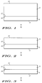
- FIG. 1 illustrates a highly enlarged cross-sectional view of a semiconductor wafer 11 to which support film 15 is bonded or attached in accordance with the present invention.
- a roll of support film 15 is placed on a peripheral portion of front-side 12 with contact surface 16 facing front-side 12.
- Support film 15 is rolled across front-side 12 from one edge located at the peripheral portion of semiconductor wafer 11 to an opposite edge.
- the act of rolling support film 15 across front-side 12 bonds or attaches to contact surface 16 and front-side 12 together without voids, thereby forming a mounted wafer 10.
- semiconductor wafer 11 may be placed on a vacuum chuck wherein the vacuum is enabled.
- support film 15 may be applied by hand or using a low-tension tape distribution apparatus. However, it is desirable that support film 15 not have any wrinkles. Further, the bonding of contact surface 16 and front-side 12 provides a substantially zero stress bond that does not significantly bow or warp semiconductor wafer 11 in its thinned state. If a vacuum chuck is used, the vacuum is disabled allowing removal of mounted wafer 10 from the vacuum chuck.
- Support film 15 provides support for semiconductor wafer 11 as well as covering front side 12, and providing protection for front-side 12 during the wafer thinning steps. Thus, support film 15 serves as a handle for subsequent wafer processing steps.
- a variety of methods for thinning semiconductor wafer 11 are available including mechanical grinding, lapping, chemical etching, and a combination mechanical grinding/chemical etching or lapping/chemical etching. It shall be understood that the step of thinning includes removing a desired thickness from semiconductor wafer 11 wherein the desired thickness is removed from back-side 13. Since mechanical grinding introduces a grinder induced stress, it is preferable that a combination of mechanical grinding and a chemical etching be performed to accomplish wafer thinning in accordance with the present invention.
- semiconductor wafer 11 comprising gallium arsenide and having a thickness of approximately 625 ⁇ m, is thinned by mechanical grinding to a thickness of approximately 400 ⁇ m (approximately 16 mils). Thus a desired thickness of approximately 225 ⁇ m is removed from back-side 13. It shall be understood that although semiconductor wafer 11 is thinned to a thickness of approximately 400 ⁇ m, mechanical grinding can be used to grind semiconductor wafer 11 to a thickness of approximately 250 ⁇ m. At thicknesses less than approximately 250 ⁇ m, a gallium arsenide semiconductor wafer becomes extremely fragile. An advantage of mechanical grinding is that this technique is a fast and accurate way to thin a semiconductor wafer.
- a semiconductor wafer 11 comprising silicon may be mechanically thinned to approximately 50 ⁇ m before becoming susceptible to breakage due to its fragility.
- FIG. 2 illustrates a highly enlarged cross-sectional view of semiconductor wafer 11 and support film 15 of FIG. 1 after the step of mechanically grinding back-side 13.
- back-side 13 is subjected to chemical etching.
- the chemical etching is performed in a single sided spray spin etcher such as, for example, an APT model 9165.
- An advantage in using a single sided spray spin etcher like the APT model 9165 is that it has a plurality of dispense ports which are microprocessor controlled thereby permitting a plurality of chemical etching steps without removing the mounted wafer 10 from the system.
- mounted wafer 10 is placed in the spray spin etcher.
- the spray spin etcher is enabled and an etchant comprising a mixture of sulfuric acid, hydrogen peroxide, and water is dispensed from a first dispense port to back-side 13.
- semiconductor wafer 11 is etched to a thickness ranging between approximately 50 and 360 ⁇ m (approximately 2 and 14 mils, respectively) using a chemical etchant such as the one described.
- the composition of the chemical etchant is not a limitation of the present invention.
- the etching of semiconductor wafer 11 is terminated by stopping the flow of etchant from the first dispense port and starting the flow of a cleaning solution comprising, for example, ammonium hydroxide and water from a second dispense port. It shall be understood that a thickness to which semiconductor wafer 11 is thinned or etched is not a limitation of the present invention.
- FIG. 3 illustrates a highly enlarged cross-sectional view of mounted wafer 10 after the step of chemically etching.
- the step of chemically etching using a spray spin etcher is not limited to a single sided spray spin etcher or to an APT model 9165.
- a batch Semitool spray etcher, or spray spin etching using models other than the APT model 9165 may be used to accomplish the step of chemical etching.
- semiconductor wafer 11 is thinned using the mechanical grinding technique of the first example followed by chemical etching.
- chemical etching is performed in an etch bath rather than a spray spin etcher.
- Methods for etching semiconductor wafers in an etch bath are well known to those skilled in the art.
- FIG. 4 illustrates a highly enlarged cross-sectional view of mounted wafer 10 having a metal layer 18 sputtered onto back-side 13 of semiconductor wafer 11.
- Metal film 18 may be, for example, a nickel-vanadium layer having a thickness of approximately 300 nanometers and a gold layer having a thickness of approximately 100 nanometers.
- FIG. 5 illustrates a highly enlarged cross-sectional view of a thinned wafer 11 having a metal film 18 mounted to a tape frame 20 and partial removal of support film 15
- tape frame 20 comprises a circular molded plastic ring 21 across which an adhesive tape 22 is stretched taut.
- Thinned wafer 11 is mounted to tape frame 20 in preparation for dicing.
- Tape frames and methods for mounting semiconductor wafers such as thinned wafer 11 to tape frames are well known and commonly used in wafer dicing operations.
- support film 15 is separated or removed from front-side 12 after mounting to support 20.
- Tape frame 20 provides support to semiconductor wafer 11 after support film 15 is removed.
- Support film 15 may be removed by peeling the film as indicated by arrow 21 of FIG. 5. Peeling support film 15 may be accomplished manually using, for example, vacuum tweezers, or an automated process.
- the present invention provides a method for thinning semiconductor wafers, thus increasing a thermal dissipation capability of semiconductor wafers.
- the method provides both structural support and front-side wafer protection throughout all the processing steps. More particularly, the support film providing these features may remain attached to the semiconductor wafer until the wafer is mounted in a tape frame, thus the semiconductor wafer is never in an unsupported state.
- the support provided by the support film or handle permits cassette to cassette handling of the mounted wafer such as those used in automated wafer handling systems.
- the thermal properties of the support film allow the mounted wafer to undergo high temperature processing steps such as, for example, back metal sputter deposition.
- the present invention also provides a method for thinning wafers that decreases the number of processing steps required to thin a wafer, thereby decreasing both cycle time and the monetary costs associated with wafer thinning.
Abstract
Description
- This invention relates, in general, to methods of processing a semiconductor wafer, and more particularly to methods of thinning a semiconductor wafer.
- Semiconductor wafer thinning techniques have been developed in response to the ever increasing demand for smaller, higher performance semiconductor devices. For example, semiconductor devices operated at high speeds generate large amounts of heat. This heat must be removed from the semiconductor device to prevent device failure due to heat stress and to prevent degradation of the frequency response due to a decrease in carrier mobility. One way to enhance thermal transfer away from the semiconductor device, thereby mitigating any deleterious temperature effects, is by thinning the semiconductor wafer in which the device is fabricated. Other reasons for thinning a semiconductor wafer include dimensional packaging constraints, optimization of transmission line characteristics, and formation of via holes.
- Typically, semiconductor devices are thinned while the devices are in wafer form. A consequence of thinning a semiconductor wafer is to increase its fragility. Thus, a semiconductor wafer is generally mounted to a submount prior to thinning, wherein the submount provides structural support as well as protection for the wafer surface. A first step in mounting a semiconductor wafer to the submount is coating a major surface of the wafer with an adhesive material. The adhesive coated major surface is bonded to the submount, thereby forming a bonded wafer. In addition to providing structural support for the semiconductor wafer the submount may serve as a handle. An example of a technique for applying an adhesive material to a semiconductor wafer and mounting the semiconductor wafer to a submount may be found in U.S. Patent Number 3,475,867 entitled "Processing of Semiconductor Wafers," and in U.S. Patent Number 3,492,763 entitled "Method and Apparatus for Mounting Semiconductor Slices," respectively.
- The bonded wafer is thinned by either mechanically grinding or chemically etching an exposed surface of the semiconductor wafer. The adhesive material bonding the semiconductor wafer to the submount must provide a bond capable of withstanding the shearing forces generated by mechanical grinding, the reactivity of a chemical etchant, and temperatures associated with semiconductor wafer processing.
- Although methods for thinning semiconductor wafers are known, they are not without limitations. For example, the step of mounting a semiconductor wafer to a submount requires expensive coating and bonding equipment and increases the overall processing time for manufacturing a semiconductor device, i.e. increases the cycle time. Further, the use of liquid adhesive materials increases the potential for introducing contaminants into the process area. In addition, the processing temperatures which the bonded wafer encounters must remain below the melting temperature of the adhesive material. Other limitations include the warping or bowing of semiconductor wafers due to mismatches between the coefficients of thermal expansion of the wafer and the submount, complications in automatic wafer handling due to the thickness of the bonded wafer, and having an unsupported wafer upon separation of the wafer and the submount.
- Accordingly, it would be advantageous to have a method for thinning a semiconductor wafer having an optimized number of processing steps and which is compatible with automated wafer handling systems. The method should decrease the cycle time required for processing a semiconductor wafer and be capable of employing either mechanical grinding, chemical etching, or a combination of the two. Further, it is desirable that the method provide a handle to eliminate any unsupported wafer handling that may occur after the wafer has been thinned and that the handle continue to provide support at temperatures used for sputter deposition of metals.
- Briefly stated, the present invention is a method for thinning a semiconductor wafer. A semiconductor wafer having a first major surface and a second major surface is provided. A support film having a first major surface which has an adhesive strength of less than approximately 20 grams per 25 millimeters of support film width at a 90 degree pulling angle is provided. The support film is capable of withstanding temperatures up to approximately 200 degrees Celsius. The first major surface of the support film is bonded with the first major surface of the semiconductor wafer. A desired thickness of the semiconductor wafer is removed from the second major surface. Subsequently, the support film is separated from the semiconductor wafer.
-
- FIG. 1 illustrates a highly enlarged cross-sectional view of a semiconductor wafer to which a support film is bonded in accordance with the present invention;
- FIG. 2 illustrates a highly enlarged cross-sectional view of the semiconductor wafer and support film of FIG. 1 after a mechanical thinning step in accordance with the present invention;
- FIG. 3 illustrates a highly enlarged cross-sectional view of the semiconductor wafer and support film of FIG. 2 after a chemical thinning step in accordance with the present invention;
- FIG. 4 illustrates a highly enlarged cross-sectional view of the semiconductor wafer and support film of FIG. 3 after metallization of a surface of the semiconductor wafer; and
- FIG. 5 illustrates a highly enlarged cross-sectional view of a thinned semiconductor wafer mounted to a tape frame and partial removal of the support film in accordance with the present invention.
- A
substrate 11 such as a semiconductor wafer (shown in FIG. 1) having amajor surface 12 and amajor surface 13 is provided. Semiconductor devices are fabricated onmajor surface 12 which is hereby defined herein as a front-side ofsemiconductor wafer 11.Major surface 13, commonly referred to as a back-side, is a portion that will be removed by mechanical grinding or chemical etching. Preferably,semiconductor wafer 11 is a gallium arsenide semiconductor wafer having a thickness of approximately 625 micrometers (approximately 24.6 mils) It shall be understood that the type of semiconductor material forsemiconductor wafer 11 and its initial thickness are not limitations of the present invention. For example,semiconductor wafer 11 may be silicon, silicon germanium, indium phosphide, or the like. - In addition, a support film 15 (shown in FIG. 1) having a
major surface 16 and amajor surface 17 is provided.Support film 15 is also referred to as a handle, a film, or a tape. Preferably,major surface 16 comprises a low-tack contact material capable of adhering to smooth surfaces. A smooth surface in the context of the present invention includes semiconductor wafers comprising semiconductor materials such as those mentioned previously, wherein one side of each semiconductor wafer has been processed to have semiconductor devices therein. Asuitable support film 15 is a tape having a part number WF-55-X4-HT sold as a Gel-Pak™ product line herein referred to as the support film. Gel-Pak™ is a trademark of the Chip Carrier Shipping System Division of Vichem Corporation. The Chip Carrier Shipping System Division of Vichem Corporation is located at 756 North Pastoria Avenue, Sunnyvale, California 94086. The tape or support film comprises a polyester layer having a thickness of approximately 127 µm (approximately 5 mils), a contact layer comprising a resilient silicone rubber having a thickness of approximately 153 µm (approximately 6 mils) and an interlayer therebetween comprising aluminum having a thickness of less than approximately 0.01 µm (approximately 100 angstroms). The aluminum interlayer provides additional stiffness, uniform temperature distribution, electrostatic discharge protection, and promotes adhesion between the polyester layer and the silicone rubber layer. Althoughsupport film 15 having part number WF-55-X4-HT is preferred and has an aluminum interlayer, it shall be understood that the aluminum interlayer is optional. - Typically, tapes are not used to provide support because they have an unacceptably high adhesive strength, degrade at temperatures used, for example, in metal sputter deposition processes, and provide a compressive stress to thinned semiconductor wafers such that they tend to bow or break the thinned semiconductor wafers. The Gel-Pak™ support
film 15, however, is a heat stable film capable of withstanding temperatures up to approximately 200 degrees Celsius (°C). The ability of supportfilm 15 to withstand temperatures up to approximately 200 °C enables its use in subsequent high temperature wafer processing steps such as back metal sputter deposition. Further,support film 15 is readily removed from, for example, a semiconductor wafer by peeling, wherein the support film has sufficient shear strength that it does not tear or separate and leave a portion on the semiconductor wafer. In addition, a thinned semiconductor wafer is not broken or otherwise damaged during the removal of the support film. - Although an adhesive strength or tackiness is not provided for the Gel-Pak™
support film 15 it is believed to have an adhesive strength less than approximately 20 grams per 25 millimeters of film width at a 90 degree pulling angle. Thus, films encompassed by the scope of the present invention include those capable of withstanding a temperature up to approximately 200°C, having an adhesive strength less than approximately 20 grams per 25 millimeters of film width at a 90 degree pulling angle, and providing substantially zero compressive stress to a substrate such as a thinned semiconductor wafer. - FIG. 1 illustrates a highly enlarged cross-sectional view of a
semiconductor wafer 11 to which supportfilm 15 is bonded or attached in accordance with the present invention. A roll ofsupport film 15 is placed on a peripheral portion of front-side 12 withcontact surface 16 facing front-side 12.Support film 15 is rolled across front-side 12 from one edge located at the peripheral portion ofsemiconductor wafer 11 to an opposite edge. The act of rollingsupport film 15 across front-side 12 bonds or attaches to contactsurface 16 and front-side 12 together without voids, thereby forming a mountedwafer 10. To facilitate bonding ofsupport film 15 tosemiconductor wafer 11,semiconductor wafer 11 may be placed on a vacuum chuck wherein the vacuum is enabled. It shall be understood that the method forbonding support film 15 tosemiconductor wafer 11 is not a limitation of the present invention. In other words,support film 15 may be applied by hand or using a low-tension tape distribution apparatus. However, it is desirable thatsupport film 15 not have any wrinkles. Further, the bonding ofcontact surface 16 and front-side 12 provides a substantially zero stress bond that does not significantly bow orwarp semiconductor wafer 11 in its thinned state. If a vacuum chuck is used, the vacuum is disabled allowing removal of mountedwafer 10 from the vacuum chuck. -
Support film 15 provides support forsemiconductor wafer 11 as well as coveringfront side 12, and providing protection for front-side 12 during the wafer thinning steps. Thus,support film 15 serves as a handle for subsequent wafer processing steps. A variety of methods for thinningsemiconductor wafer 11 are available including mechanical grinding, lapping, chemical etching, and a combination mechanical grinding/chemical etching or lapping/chemical etching. It shall be understood that the step of thinning includes removing a desired thickness fromsemiconductor wafer 11 wherein the desired thickness is removed from back-side 13. Since mechanical grinding introduces a grinder induced stress, it is preferable that a combination of mechanical grinding and a chemical etching be performed to accomplish wafer thinning in accordance with the present invention. In a first example,semiconductor wafer 11, comprising gallium arsenide and having a thickness of approximately 625 µm, is thinned by mechanical grinding to a thickness of approximately 400 µm (approximately 16 mils). Thus a desired thickness of approximately 225 µm is removed from back-side 13. It shall be understood that althoughsemiconductor wafer 11 is thinned to a thickness of approximately 400 µm, mechanical grinding can be used to grindsemiconductor wafer 11 to a thickness of approximately 250 µm. At thicknesses less than approximately 250 µm, a gallium arsenide semiconductor wafer becomes extremely fragile. An advantage of mechanical grinding is that this technique is a fast and accurate way to thin a semiconductor wafer. Thus, fragility of the gallium arsenide semiconductor wafer places a constraint to which a gallium arsenide semiconductor wafer can be thinned using a mechanical grinding technique. Asemiconductor wafer 11 comprising silicon, on the other hand, may be mechanically thinned to approximately 50 µm before becoming susceptible to breakage due to its fragility. - Methods for grinding wafers are well known in the art. A mechanical grinding method suitable for use in the present invention is described by Hishiguchi et al in their article "Mass Production Back-Grinding/Wafer-Thinning Technology for GaAs Devices" published in the IEEE Transaction on Components, Hybrids, and Manufacturing Technology,
Vol 13, No. 3, September 1990. - FIG. 2 illustrates a highly enlarged cross-sectional view of
semiconductor wafer 11 andsupport film 15 of FIG. 1 after the step of mechanically grinding back-side 13. - To relieve grinder induced stress and to further
thin semiconductor wafer 11, back-side 13 is subjected to chemical etching. Preferably, the chemical etching is performed in a single sided spray spin etcher such as, for example, an APT model 9165. An advantage in using a single sided spray spin etcher like the APT model 9165 is that it has a plurality of dispense ports which are microprocessor controlled thereby permitting a plurality of chemical etching steps without removing the mountedwafer 10 from the system. In a first step, mountedwafer 10 is placed in the spray spin etcher. The spray spin etcher is enabled and an etchant comprising a mixture of sulfuric acid, hydrogen peroxide, and water is dispensed from a first dispense port to back-side 13. Preferably,semiconductor wafer 11 is etched to a thickness ranging between approximately 50 and 360 µm (approximately 2 and 14 mils, respectively) using a chemical etchant such as the one described. The composition of the chemical etchant is not a limitation of the present invention. The etching ofsemiconductor wafer 11 is terminated by stopping the flow of etchant from the first dispense port and starting the flow of a cleaning solution comprising, for example, ammonium hydroxide and water from a second dispense port. It shall be understood that a thickness to whichsemiconductor wafer 11 is thinned or etched is not a limitation of the present invention. - The cleaning step is followed by a rinse with de-ionized water. The de-ionized water is dispensed from a third dispense port.
Semiconductor wafer 11 is dried using, for example, nitrogen. FIG. 3 illustrates a highly enlarged cross-sectional view of mountedwafer 10 after the step of chemically etching. - It shall be understood that the step of chemically etching using a spray spin etcher is not limited to a single sided spray spin etcher or to an APT model 9165. In other words a batch Semitool spray etcher, or spray spin etching using models other than the APT model 9165 may be used to accomplish the step of chemical etching.
- In a second example,
semiconductor wafer 11 is thinned using the mechanical grinding technique of the first example followed by chemical etching. However, in this example the chemical etching is performed in an etch bath rather than a spray spin etcher. Methods for etching semiconductor wafers in an etch bath are well known to those skilled in the art. - After drying, mounted
wafer 10 is ready for subsequent processing. In one embodiment, mountedwafer 10 is placed in a back metal sputter system for sputter deposition of a metal film. FIG. 4 illustrates a highly enlarged cross-sectional view of mountedwafer 10 having ametal layer 18 sputtered onto back-side 13 ofsemiconductor wafer 11. Methods of sputtering layers of metal on semiconductor wafers, such assemiconductor wafer 11 are well known in the art.Metal film 18 may be, for example, a nickel-vanadium layer having a thickness of approximately 300 nanometers and a gold layer having a thickness of approximately 100 nanometers. - FIG. 5 illustrates a highly enlarged cross-sectional view of a thinned
wafer 11 having ametal film 18 mounted to atape frame 20 and partial removal ofsupport film 15 In one embodiment,tape frame 20 comprises a circular moldedplastic ring 21 across which anadhesive tape 22 is stretched taut. Thinnedwafer 11 is mounted totape frame 20 in preparation for dicing. Tape frames and methods for mounting semiconductor wafers such as thinnedwafer 11 to tape frames are well known and commonly used in wafer dicing operations. Preferably,support film 15 is separated or removed from front-side 12 after mounting to support 20.Tape frame 20 provides support tosemiconductor wafer 11 aftersupport film 15 is removed.Support film 15 may be removed by peeling the film as indicated byarrow 21 of FIG. 5. Peelingsupport film 15 may be accomplished manually using, for example, vacuum tweezers, or an automated process. - By now it should be appreciated that the present invention provides a method for thinning semiconductor wafers, thus increasing a thermal dissipation capability of semiconductor wafers. The method provides both structural support and front-side wafer protection throughout all the processing steps. More particularly, the support film providing these features may remain attached to the semiconductor wafer until the wafer is mounted in a tape frame, thus the semiconductor wafer is never in an unsupported state. Moreover, the support provided by the support film or handle permits cassette to cassette handling of the mounted wafer such as those used in automated wafer handling systems.
- Further, the thermal properties of the support film allow the mounted wafer to undergo high temperature processing steps such as, for example, back metal sputter deposition. The present invention also provides a method for thinning wafers that decreases the number of processing steps required to thin a wafer, thereby decreasing both cycle time and the monetary costs associated with wafer thinning.
Claims (10)
- A method for thinning a semiconductor wafer (11), characterized in that:
providing the semiconductor wafer (11), wherein the semiconductor wafer (11) has a first major surface (12) and a second major surface (13);
providing a support film (15) capable of withstanding a temperature up to approximately 200 degrees Celsius, and having a first major surface (16) and a second major surface (17), wherein the first major surface (16) has an adhesive strength less than approximately 20 gram per 25 millimeters of support film width at a 90 degree pulling angle;
bonding the first major surface (16) of the support film (15) with the first major surface (12) of the semiconductor wafer (11);
removing a desired thickness from the semiconductor wafer (11) wherein the desired thickness is removed from a side of the semiconductor wafer (11) having the second major surface (13); and
separating the first major surface (16) of the support film (15) from the first major surface (12) of the semiconductor wafer (11). - A method for thinning a semiconductor wafer as claimed in claim 1 wherein the step of bonding the first major surface (16) of the support film (15) with the first major surface (12) of the semiconductor wafer (11) includes rolling the support film (15) onto the semiconductor wafer (11).
- A method for thinning a substrate (11), characterized in that:
providing the substrate (11), wherein the substrate (11) has a first major surface (12) and a second major surface (13);
providing a handle (15) having an adhesive strength less than approximately 20 grams per 25 millimeters of handle width at a 90 degree pulling angle;
covering the first major surface (12) with the handle (15);
removing a desired thickness from the substrate (11) wherein the desired thickness is removed from a side of the substrate (11) having the second major surface (13); and
removing the handle (15) from the first major surface (12) of the substrate (11). - A method for thinning a substrate (11) as claimed in claim 3 wherein the step of providing a handle (15) includes providing a handle (15) capable of withstanding temperatures ranging up to, approximately, 200 degrees Celsius.
- A method for thinning a substrate (11) as claimed in claim 3 wherein the step of removing a desired thickness from the substrate (11) includes the steps of:
mechanically grinding a desired thickness of the second major surface (13) of the substrate (11); and
chemically etching a desired thickness of the second major surface (13) of the substrate (11) . - A method for thinning a substrate (11) as claimed in claim 5 wherein the step of chemically etching the desired thickness includes the steps of:
etching the substrate (11) with a first solution, the first solution comprising sulfuric acid, hydrogen peroxide, and water;
cleaning the substrate (11) with a second solution, the second solution comprising ammonium hydroxide, and water;
rinsing the substrate (11) with water; and
drying the substrate (11). - A method for increasing a thermal dissipation capability of a semiconductor wafer (11), characterized in that:
providing the semiconductor wafer (11) having a first major surface (12) and a second major surface (13);
attaching a support film (15) to the first major surface (12) of the semiconductor wafer (11);
thinning the semiconductor wafer (11);
providing a metallic film (18) on the second major surface (13) of the semiconductor wafer (11); and
peeling the support film (15) from the first major surface (12) of the semiconductor wafer (11) - A method for increasing a thermal dissipation capability of a semiconductor wafer (11) as claimed in claim 7 wherein the step of attaching a support film (15) to the first major surface (12) of the semiconductor wafer (11) includes providing a support film (15), the support film (15) capable of withstanding temperatures ranging up to, approximately, 200 degrees Celsius.
- A method for increasing a thermal dissipation capability of a semiconductor wafer (11) as claimed in claim 7 wherein the step of peeling the support film (15) includes mounting the support film (15) in a tape frame (20) followed by peeling the support film (15).
- A method for increasing a thermal dissipation capability of a semiconductor wafer (11) as claimed in claim 7 wherein the step of attaching a support film (15) to the first major surface (12) of the semiconductor wafer (11) includes the steps of:
placing a portion of a first major surface (16) of the support film (15) on a peripheral portion of the first major surface (12) of the semiconductor wafer (11); and
rolling the support film (15) from one edge at the peripheral portion to an opposite edge of the first major surface (12) of the semiconductor wafer (11), wherein the step of rolling bonds the support film (15) to the semiconductor wafer (11)
Applications Claiming Priority (2)
| Application Number | Priority Date | Filing Date | Title |
|---|---|---|---|
| US993984 | 1992-12-21 | ||
| US07/993,984 US5268065A (en) | 1992-12-21 | 1992-12-21 | Method for thinning a semiconductor wafer |
Publications (2)
| Publication Number | Publication Date |
|---|---|
| EP0603514A2 true EP0603514A2 (en) | 1994-06-29 |
| EP0603514A3 EP0603514A3 (en) | 1995-07-26 |
Family
ID=25540154
Family Applications (1)
| Application Number | Title | Priority Date | Filing Date |
|---|---|---|---|
| EP93117874A Withdrawn EP0603514A3 (en) | 1992-12-21 | 1993-11-04 | Method for thinning a semiconductor wafer. |
Country Status (3)
| Country | Link |
|---|---|
| US (1) | US5268065A (en) |
| EP (1) | EP0603514A3 (en) |
| JP (1) | JPH06224095A (en) |
Cited By (6)
| Publication number | Priority date | Publication date | Assignee | Title |
|---|---|---|---|---|
| EP1054437A2 (en) * | 1999-05-21 | 2000-11-22 | Tokyo Seimitsu Co.,Ltd. | Method and apparatus for attaching wafer to wafer frame and planarization apparatus including attaching apparatus |
| EP1089326A2 (en) * | 1999-09-29 | 2001-04-04 | Shin-Etsu Chemical Co., Ltd. | Wafer support with a dustproof covering film and method for producing the same |
| US6573156B1 (en) | 2001-12-13 | 2003-06-03 | Omm, Inc. | Low defect method for die singulation and for structural support for handling thin film devices |
| DE102011079687A1 (en) | 2011-07-22 | 2013-01-24 | Wacker Chemie Ag | Temporary bonding of chemically similar substrates |
| WO2014075879A1 (en) | 2012-11-16 | 2014-05-22 | Wacker Chemie Ag | Abradable silicone elastomer compound and use thereof |
| CN107180781A (en) * | 2016-03-10 | 2017-09-19 | 东芝存储器株式会社 | The manufacture method of semiconductor device |
Families Citing this family (71)
| Publication number | Priority date | Publication date | Assignee | Title |
|---|---|---|---|---|
| DE4411409C2 (en) * | 1994-03-31 | 1998-05-14 | Siemens Ag | Process for backside thinning of structured silicon wafers |
| US5480842A (en) * | 1994-04-11 | 1996-01-02 | At&T Corp. | Method for fabricating thin, strong, and flexible die for smart cards |
| US6153891A (en) * | 1994-11-23 | 2000-11-28 | Intel Corporation | Method and apparatus providing a circuit edit structure through the back side of an integrated circuit die |
| US5976980A (en) * | 1994-11-23 | 1999-11-02 | Intel Corporation | Method and apparatus providing a mechanical probe structure in an integrated circuit die |
| US6020746A (en) * | 1994-11-23 | 2000-02-01 | Intel Corporation | Method and apparatus for probing an integrated circuit through the back side of an integrated circuit die |
| US5952247A (en) * | 1994-11-23 | 1999-09-14 | Intel Corporation | Method of accessing the circuitry on a semiconductor substrate from the bottom of the semiconductor substrate |
| DE19505906A1 (en) * | 1995-02-21 | 1996-08-22 | Siemens Ag | Process for damaging the back of a semiconductor wafer with the front of the wafer protected |
| JP3197788B2 (en) | 1995-05-18 | 2001-08-13 | 株式会社日立製作所 | Method for manufacturing semiconductor device |
| US5875110A (en) | 1995-06-07 | 1999-02-23 | American Greetings Corporation | Method and system for vending products |
| US6342434B1 (en) * | 1995-12-04 | 2002-01-29 | Hitachi, Ltd. | Methods of processing semiconductor wafer, and producing IC card, and carrier |
| US6083811A (en) * | 1996-02-07 | 2000-07-04 | Northrop Grumman Corporation | Method for producing thin dice from fragile materials |
| JP3993918B2 (en) * | 1997-08-25 | 2007-10-17 | 富士通株式会社 | Manufacturing method of semiconductor device |
| US5904486A (en) * | 1997-09-30 | 1999-05-18 | Intel Corporation | Method for performing a circuit edit through the back side of an integrated circuit die |
| US6309897B1 (en) | 1997-09-30 | 2001-10-30 | Intel Corporation | Method and apparatus providing a circuit edit structure through the back side of an integrated circuit die |
| TW425625B (en) * | 1997-11-18 | 2001-03-11 | Mitsui Chemicals Inc | Method of producing semiconductor wafer |
| AU3144899A (en) * | 1998-03-14 | 1999-10-11 | Michael Stromberg | Method and device for treating wafers presenting components during thinning of the wafer and separation of the components |
| US6159827A (en) * | 1998-04-13 | 2000-12-12 | Mitsui Chemicals, Inc. | Preparation process of semiconductor wafer |
| US6159754A (en) * | 1998-05-07 | 2000-12-12 | Intel Corporation | Method of making a circuit edit interconnect structure through the backside of an integrated circuit die |
| US6153536A (en) * | 1999-03-04 | 2000-11-28 | International Business Machines Corporation | Method for mounting wafer frame at back side grinding (BSG) tool |
| US6320269B1 (en) | 1999-05-03 | 2001-11-20 | Taiwan Semiconductor Manufacturing Company | Method for preparing a semiconductor wafer to receive a protective tape |
| DE19921230B4 (en) * | 1999-05-07 | 2009-04-02 | Giesecke & Devrient Gmbh | Method for handling thinned chips for insertion in chip cards |
| US6391220B1 (en) | 1999-08-18 | 2002-05-21 | Fujitsu Limited, Inc. | Methods for fabricating flexible circuit structures |
| US6448106B1 (en) | 1999-11-09 | 2002-09-10 | Fujitsu Limited | Modules with pins and methods for making modules with pins |
| JP2001157959A (en) | 1999-11-30 | 2001-06-12 | Tokyo Seimitsu Co Ltd | Surface grinding apparatus |
| US6368881B1 (en) | 2000-02-29 | 2002-04-09 | International Business Machines Corporation | Wafer thickness control during backside grind |
| JP2001345300A (en) * | 2000-05-31 | 2001-12-14 | Disco Abrasive Syst Ltd | Semiconductor wafer machining body and machining apparatus comprising chuck table for holding semiconductor wafer machining body |
| US6465353B1 (en) * | 2000-09-29 | 2002-10-15 | International Rectifier Corporation | Process of thinning and blunting semiconductor wafer edge and resulting wafer |
| US6506681B2 (en) | 2000-12-06 | 2003-01-14 | Micron Technology, Inc. | Thin flip—chip method |
| US6730595B2 (en) * | 2000-12-12 | 2004-05-04 | Mitsui Chemicals, Inc. | Protecting method for semiconductor wafer and surface protecting adhesive film for semiconductor wafer used in said method |
| KR100383265B1 (en) * | 2001-01-17 | 2003-05-09 | 삼성전자주식회사 | Semiconductor processing apparatus to remove wafer protection tape |
| AT502233B1 (en) * | 2001-06-07 | 2007-04-15 | Thallner Erich | Carrier detachment device aligns inner, near-edge surface of frame with semiconductor disk and bonds them to foil, before detaching disk from carrier |
| US20030006493A1 (en) * | 2001-07-04 | 2003-01-09 | Matsushita Electric Industrial Co., Ltd. | Semiconductor device and manufacturing method thereof |
| US6743722B2 (en) * | 2002-01-29 | 2004-06-01 | Strasbaugh | Method of spin etching wafers with an alkali solution |
| US6692995B2 (en) | 2002-04-05 | 2004-02-17 | Intel Corporation | Physically deposited layer to electrically connect circuit edit connection targets |
| US6614117B1 (en) * | 2002-06-04 | 2003-09-02 | Skyworks Solutions, Inc. | Method for metallization of a semiconductor substrate and related structure |
| US6713366B2 (en) * | 2002-06-12 | 2004-03-30 | Intel Corporation | Method of thinning a wafer utilizing a laminated reinforcing layer over the device side |
| JP2004079889A (en) * | 2002-08-21 | 2004-03-11 | Disco Abrasive Syst Ltd | Manufacturing method of semiconductor wafer |
| JP2004119718A (en) * | 2002-09-26 | 2004-04-15 | Shinko Electric Ind Co Ltd | Method of manufacturing thin semiconductor chip |
| DE10256247A1 (en) * | 2002-11-29 | 2004-06-09 | Andreas Jakob | Process for treating wafers comprises covering the front side of the wafer having components with a layer system consisting of a separating layer and a protective layer before the rear side of the wafer is coated |
| WO2004051708A2 (en) * | 2002-11-29 | 2004-06-17 | Fraunhofer-Gesellschaft zur Förderung der angewandten Forschung e.V. | Method and device for machining a wafer, in addition to a wafer comprising a separation layer and a support layer |
| JP4013753B2 (en) * | 2002-12-11 | 2007-11-28 | 松下電器産業株式会社 | Semiconductor wafer cutting method |
| US6869894B2 (en) | 2002-12-20 | 2005-03-22 | General Chemical Corporation | Spin-on adhesive for temporary wafer coating and mounting to support wafer thinning and backside processing |
| JP4544876B2 (en) * | 2003-02-25 | 2010-09-15 | 三洋電機株式会社 | Manufacturing method of semiconductor device |
| JP4502955B2 (en) * | 2003-09-01 | 2010-07-14 | 三井化学株式会社 | Adhesive film and metal film forming method using the same |
| US7713841B2 (en) * | 2003-09-19 | 2010-05-11 | Micron Technology, Inc. | Methods for thinning semiconductor substrates that employ support structures formed on the substrates |
| US20050064679A1 (en) * | 2003-09-19 | 2005-03-24 | Farnworth Warren M. | Consolidatable composite materials, articles of manufacture formed therefrom, and fabrication methods |
| US20050064683A1 (en) * | 2003-09-19 | 2005-03-24 | Farnworth Warren M. | Method and apparatus for supporting wafers for die singulation and subsequent handling |
| US7244665B2 (en) * | 2004-04-29 | 2007-07-17 | Micron Technology, Inc. | Wafer edge ring structures and methods of formation |
| US6984876B2 (en) * | 2004-05-27 | 2006-01-10 | Semiconductor Components Industries, L.L.C. | Semiconductor device formed having a metal layer for conducting the device current and for high contrast marking and method thereof |
| JP2005340655A (en) * | 2004-05-28 | 2005-12-08 | Shinko Electric Ind Co Ltd | Method for manufacturing semiconductor device, and structure for supporting semiconductor substrate |
| US20060040111A1 (en) * | 2004-08-20 | 2006-02-23 | Dolechek Kert L | Process chamber and system for thinning a semiconductor workpiece |
| US7354649B2 (en) | 2004-08-20 | 2008-04-08 | Semitool, Inc. | Semiconductor workpiece |
| US7193295B2 (en) * | 2004-08-20 | 2007-03-20 | Semitool, Inc. | Process and apparatus for thinning a semiconductor workpiece |
| US7288489B2 (en) * | 2004-08-20 | 2007-10-30 | Semitool, Inc. | Process for thinning a semiconductor workpiece |
| US20060046499A1 (en) * | 2004-08-20 | 2006-03-02 | Dolechek Kert L | Apparatus for use in thinning a semiconductor workpiece |
| US7244663B2 (en) * | 2004-08-31 | 2007-07-17 | Micron Technology, Inc. | Wafer reinforcement structure and methods of fabrication |
| US7413915B2 (en) * | 2004-12-01 | 2008-08-19 | Lexmark International, Inc. | Micro-fluid ejection head containing reentrant fluid feed slots |
| US7126825B2 (en) * | 2004-12-07 | 2006-10-24 | Cleavage Enterprise Co., Ltd. | Combined chip/heat-dissipating metal plate and method for manufacturing the same |
| US8124455B2 (en) * | 2005-04-02 | 2012-02-28 | Stats Chippac Ltd. | Wafer strength reinforcement system for ultra thin wafer thinning |
| DE102006004834B4 (en) * | 2005-07-15 | 2016-04-21 | Thin Materials Ag | Process for treating wafers during thinning |
| JP4937674B2 (en) * | 2006-08-16 | 2012-05-23 | 株式会社ディスコ | Wafer etching method |
| US7802359B2 (en) * | 2007-12-27 | 2010-09-28 | Freescale Semiconductor, Inc. | Electronic assembly manufacturing method |
| US7972969B2 (en) * | 2008-03-06 | 2011-07-05 | Taiwan Semiconductor Manufacturing Co., Ltd. | Method and apparatus for thinning a substrate |
| US7842543B2 (en) * | 2009-02-17 | 2010-11-30 | Alpha And Omega Semiconductor Incorporated | Wafer level chip scale package and method of laser marking the same |
| US8157621B2 (en) * | 2009-10-12 | 2012-04-17 | Nanya Technology Corp. | Wafer back side grinding process |
| US20130075892A1 (en) * | 2011-09-27 | 2013-03-28 | Taiwan Semiconductor Manufacturing Company, Ltd. | Method for Three Dimensional Integrated Circuit Fabrication |
| CN106206382A (en) * | 2016-08-30 | 2016-12-07 | 浙江中纳晶微电子科技有限公司 | The processing method that flake workpiece is bonded temporarily |
| KR102492533B1 (en) | 2017-09-21 | 2023-01-30 | 삼성전자주식회사 | Support substrate, Method of fabricating a semiconductor Package and Method of fabricating an electronic device |
| TWI687986B (en) * | 2018-11-16 | 2020-03-11 | 典琦科技股份有限公司 | Method for manufacturing chip package |
| US20230066183A1 (en) * | 2021-08-30 | 2023-03-02 | Taiwan Semiconductor Manufacturing Company Ltd. | Method of fabricating a semiconductor structure and semiconductor structure obtained therefrom |
| TWI819492B (en) * | 2022-02-16 | 2023-10-21 | 崇越科技股份有限公司 | Method for processing back of wafer |
Citations (8)
| Publication number | Priority date | Publication date | Assignee | Title |
|---|---|---|---|---|
| EP0157508A2 (en) * | 1984-03-12 | 1985-10-09 | Nitto Denko Corporation | Thin adhesive sheet for use in working semiconductor wafers |
| EP0185767A1 (en) * | 1984-05-29 | 1986-07-02 | MITSUI TOATSU CHEMICALS, Inc. | Film for machining wafers |
| JPS63164336A (en) * | 1986-12-26 | 1988-07-07 | Oki Electric Ind Co Ltd | Manufacture of semiconductor device |
| JPS63176265A (en) * | 1987-01-17 | 1988-07-20 | Nitto Electric Ind Co Ltd | Semiconductor wafer protecting member |
| EP0423648A1 (en) * | 1989-10-20 | 1991-04-24 | Fujitsu Limited | Wafer processing |
| EP0475259A2 (en) * | 1990-09-05 | 1992-03-18 | Sumitomo Electric Industries, Limited | Semiconductor element manufacturing process |
| EP0530729A1 (en) * | 1991-09-02 | 1993-03-10 | MITSUI TOATSU CHEMICALS, Inc. | Method for grinding back side of semiconductor wafer and pressure-sensitive adhesive tape used in said method |
| EP0539973A2 (en) * | 1991-11-01 | 1993-05-05 | The Furukawa Electric Co., Ltd. | A surface-protection method during etching |
Family Cites Families (9)
| Publication number | Priority date | Publication date | Assignee | Title |
|---|---|---|---|---|
| US3475867A (en) * | 1966-12-20 | 1969-11-04 | Monsanto Co | Processing of semiconductor wafers |
| US3492763A (en) * | 1967-09-18 | 1970-02-03 | Monsanto Co | Method and apparatus for mounting semiconductor slices |
| US3960623A (en) * | 1974-03-14 | 1976-06-01 | General Electric Company | Membrane mask for selective semiconductor etching |
| GB2027556B (en) * | 1978-07-31 | 1983-01-19 | Philips Electronic Associated | Manufacturing infra-red detectors |
| IT1175541B (en) * | 1984-06-22 | 1987-07-01 | Telettra Lab Telefon | PROCEDURE FOR EARTH CONNECTION OF PLANAR DEVICES AND INTEGRATED CIRCUITS AND PRODUCTS SO OBTAINED |
| NL8501773A (en) * | 1985-06-20 | 1987-01-16 | Philips Nv | METHOD FOR MANUFACTURING SEMICONDUCTOR DEVICES |
| US4846931A (en) * | 1988-03-29 | 1989-07-11 | Bell Communications Research, Inc. | Method for lifting-off epitaxial films |
| NL8802028A (en) * | 1988-08-16 | 1990-03-16 | Philips Nv | METHOD FOR MANUFACTURING AN APPARATUS |
| US5127984A (en) * | 1991-05-02 | 1992-07-07 | Avantek, Inc. | Rapid wafer thinning process |
-
1992
- 1992-12-21 US US07/993,984 patent/US5268065A/en not_active Expired - Lifetime
-
1993
- 1993-11-04 EP EP93117874A patent/EP0603514A3/en not_active Withdrawn
- 1993-12-17 JP JP5343287A patent/JPH06224095A/en active Pending
Patent Citations (8)
| Publication number | Priority date | Publication date | Assignee | Title |
|---|---|---|---|---|
| EP0157508A2 (en) * | 1984-03-12 | 1985-10-09 | Nitto Denko Corporation | Thin adhesive sheet for use in working semiconductor wafers |
| EP0185767A1 (en) * | 1984-05-29 | 1986-07-02 | MITSUI TOATSU CHEMICALS, Inc. | Film for machining wafers |
| JPS63164336A (en) * | 1986-12-26 | 1988-07-07 | Oki Electric Ind Co Ltd | Manufacture of semiconductor device |
| JPS63176265A (en) * | 1987-01-17 | 1988-07-20 | Nitto Electric Ind Co Ltd | Semiconductor wafer protecting member |
| EP0423648A1 (en) * | 1989-10-20 | 1991-04-24 | Fujitsu Limited | Wafer processing |
| EP0475259A2 (en) * | 1990-09-05 | 1992-03-18 | Sumitomo Electric Industries, Limited | Semiconductor element manufacturing process |
| EP0530729A1 (en) * | 1991-09-02 | 1993-03-10 | MITSUI TOATSU CHEMICALS, Inc. | Method for grinding back side of semiconductor wafer and pressure-sensitive adhesive tape used in said method |
| EP0539973A2 (en) * | 1991-11-01 | 1993-05-05 | The Furukawa Electric Co., Ltd. | A surface-protection method during etching |
Non-Patent Citations (2)
| Title |
|---|
| PATENT ABSTRACTS OF JAPAN vol. 12 no. 425 (E-681) ,10 November 1988 & JP-A-63 164336 (OKI ELECTRIC) 7 July 1988, * |
| PATENT ABSTRACTS OF JAPAN vol. 12 no. 445 (M-767) ,22 November 1988 & JP-A-63 176265 (NITTO ELECTRIC) 20 July 1988, * |
Cited By (13)
| Publication number | Priority date | Publication date | Assignee | Title |
|---|---|---|---|---|
| EP1054437A2 (en) * | 1999-05-21 | 2000-11-22 | Tokyo Seimitsu Co.,Ltd. | Method and apparatus for attaching wafer to wafer frame and planarization apparatus including attaching apparatus |
| EP1054437A3 (en) * | 1999-05-21 | 2005-01-19 | Tokyo Seimitsu Co.,Ltd. | Method and apparatus for attaching wafer to wafer frame and planarization apparatus including attaching apparatus |
| EP1089326A2 (en) * | 1999-09-29 | 2001-04-04 | Shin-Etsu Chemical Co., Ltd. | Wafer support with a dustproof covering film and method for producing the same |
| EP1089326A3 (en) * | 1999-09-29 | 2005-12-07 | Shin-Etsu Chemical Co., Ltd. | Wafer support with a dustproof covering film and method for producing the same |
| US6573156B1 (en) | 2001-12-13 | 2003-06-03 | Omm, Inc. | Low defect method for die singulation and for structural support for handling thin film devices |
| WO2013013986A2 (en) | 2011-07-22 | 2013-01-31 | Wacker Chemie Ag | Temporary adhesion of chemically similar substrates |
| DE102011079687A1 (en) | 2011-07-22 | 2013-01-24 | Wacker Chemie Ag | Temporary bonding of chemically similar substrates |
| US9034139B2 (en) | 2011-07-22 | 2015-05-19 | Wacker Chemie Ag | Temporary adhesion of chemically similar substrates |
| WO2014075879A1 (en) | 2012-11-16 | 2014-05-22 | Wacker Chemie Ag | Abradable silicone elastomer compound and use thereof |
| DE102012220954A1 (en) | 2012-11-16 | 2014-05-22 | Wacker Chemie Ag | Sandable silicone elastomer composition and use thereof |
| US9334435B2 (en) | 2012-11-16 | 2016-05-10 | Wacker Chemie Ag | Abradable silicone elastomer compound and use thereof |
| CN107180781A (en) * | 2016-03-10 | 2017-09-19 | 东芝存储器株式会社 | The manufacture method of semiconductor device |
| CN107180781B (en) * | 2016-03-10 | 2020-10-20 | 东芝存储器株式会社 | Method for manufacturing semiconductor device |
Also Published As
| Publication number | Publication date |
|---|---|
| EP0603514A3 (en) | 1995-07-26 |
| JPH06224095A (en) | 1994-08-12 |
| US5268065A (en) | 1993-12-07 |
Similar Documents
| Publication | Publication Date | Title |
|---|---|---|
| US5268065A (en) | Method for thinning a semiconductor wafer | |
| US5783022A (en) | Apparatus and methods for wafer debonding using a liquid jet | |
| KR101548173B1 (en) | Wafer temporary bonding method using Si direct bondingSDB and semiconductor device and fabricating method thereof using the same bonding method | |
| TW529095B (en) | Method of dividing wafer and manufacture of semiconductor device | |
| EP0631690B1 (en) | Method of fabricating a microelectronic device using an alternate substrate | |
| US6245677B1 (en) | Backside chemical etching and polishing | |
| JPH10154686A (en) | Method of cleaning semiconductor substrate processing device | |
| US6656820B2 (en) | Method for manufacturing a semiconductor device having a reliable thinning step | |
| JP2002270676A (en) | Method of manufacturing semiconductor device | |
| JP4040819B2 (en) | Wafer dividing method and semiconductor device manufacturing method | |
| EP1026735A2 (en) | Method of dividing a wafer and method of manufacturing a semiconductor device | |
| JP2004063645A (en) | Protection member exfoliation apparatus of semiconductor wafer | |
| CN111834280A (en) | Temporary bonding method | |
| JP2004241568A (en) | Substrate attachment/detachment device, substrate attachment/detachment method, and substrate treatment system | |
| JP2001093864A (en) | Semiconductor wafer fixing jig and method for manufacturing semiconductor device | |
| JP2003297786A (en) | Method for manufacturing semiconductor device | |
| EP1022778A1 (en) | Method of dividing a wafer and method of manufacturing a semiconductor device | |
| JPH08148452A (en) | Substrate surface protecting tape and substrate backside grinding method | |
| US6780703B2 (en) | Method for forming a semiconductor device | |
| US20190295877A1 (en) | Method of debonding work-carrier pair with thin devices | |
| JPH0697017A (en) | Manufacture of semiconductor device | |
| JPS61158145A (en) | Processing method for semiconductor substrate | |
| KR20110055977A (en) | Apartus for manufacturing semiconductor package and method for fabricating semiconductor package by using the same | |
| TWI819492B (en) | Method for processing back of wafer | |
| Kroninger et al. | Time for change in pre-assembly? The challenge of thin chips |
Legal Events
| Date | Code | Title | Description |
|---|---|---|---|
| PUAI | Public reference made under article 153(3) epc to a published international application that has entered the european phase |
Free format text: ORIGINAL CODE: 0009012 |
|
| AK | Designated contracting states |
Kind code of ref document: A2 Designated state(s): DE FR GB |
|
| PUAL | Search report despatched |
Free format text: ORIGINAL CODE: 0009013 |
|
| AK | Designated contracting states |
Kind code of ref document: A3 Designated state(s): DE FR GB |
|
| 17P | Request for examination filed |
Effective date: 19960402 |
|
| 17Q | First examination report despatched |
Effective date: 19960530 |
|
| STAA | Information on the status of an ep patent application or granted ep patent |
Free format text: STATUS: THE APPLICATION IS DEEMED TO BE WITHDRAWN |
|
| 18D | Application deemed to be withdrawn |
Effective date: 19971018 |