EP0475259A2 - Semiconductor element manufacturing process - Google Patents
Semiconductor element manufacturing process Download PDFInfo
- Publication number
- EP0475259A2 EP0475259A2 EP91114907A EP91114907A EP0475259A2 EP 0475259 A2 EP0475259 A2 EP 0475259A2 EP 91114907 A EP91114907 A EP 91114907A EP 91114907 A EP91114907 A EP 91114907A EP 0475259 A2 EP0475259 A2 EP 0475259A2
- Authority
- EP
- European Patent Office
- Prior art keywords
- grinding
- substrate
- micro
- gaas substrate
- semiconductor element
- Prior art date
- Legal status (The legal status is an assumption and is not a legal conclusion. Google has not performed a legal analysis and makes no representation as to the accuracy of the status listed.)
- Granted
Links
Images


Classifications
-
- H—ELECTRICITY
- H01—ELECTRIC ELEMENTS
- H01L—SEMICONDUCTOR DEVICES NOT COVERED BY CLASS H10
- H01L21/00—Processes or apparatus adapted for the manufacture or treatment of semiconductor or solid state devices or of parts thereof
- H01L21/02—Manufacture or treatment of semiconductor devices or of parts thereof
- H01L21/04—Manufacture or treatment of semiconductor devices or of parts thereof the devices having at least one potential-jump barrier or surface barrier, e.g. PN junction, depletion layer or carrier concentration layer
- H01L21/18—Manufacture or treatment of semiconductor devices or of parts thereof the devices having at least one potential-jump barrier or surface barrier, e.g. PN junction, depletion layer or carrier concentration layer the devices having semiconductor bodies comprising elements of Group IV of the Periodic System or AIIIBV compounds with or without impurities, e.g. doping materials
- H01L21/30—Treatment of semiconductor bodies using processes or apparatus not provided for in groups H01L21/20 - H01L21/26
- H01L21/302—Treatment of semiconductor bodies using processes or apparatus not provided for in groups H01L21/20 - H01L21/26 to change their surface-physical characteristics or shape, e.g. etching, polishing, cutting
- H01L21/306—Chemical or electrical treatment, e.g. electrolytic etching
- H01L21/30604—Chemical etching
- H01L21/30612—Etching of AIIIBV compounds
-
- H—ELECTRICITY
- H01—ELECTRIC ELEMENTS
- H01L—SEMICONDUCTOR DEVICES NOT COVERED BY CLASS H10
- H01L21/00—Processes or apparatus adapted for the manufacture or treatment of semiconductor or solid state devices or of parts thereof
- H01L21/02—Manufacture or treatment of semiconductor devices or of parts thereof
- H01L21/04—Manufacture or treatment of semiconductor devices or of parts thereof the devices having at least one potential-jump barrier or surface barrier, e.g. PN junction, depletion layer or carrier concentration layer
- H01L21/18—Manufacture or treatment of semiconductor devices or of parts thereof the devices having at least one potential-jump barrier or surface barrier, e.g. PN junction, depletion layer or carrier concentration layer the devices having semiconductor bodies comprising elements of Group IV of the Periodic System or AIIIBV compounds with or without impurities, e.g. doping materials
- H01L21/30—Treatment of semiconductor bodies using processes or apparatus not provided for in groups H01L21/20 - H01L21/26
- H01L21/302—Treatment of semiconductor bodies using processes or apparatus not provided for in groups H01L21/20 - H01L21/26 to change their surface-physical characteristics or shape, e.g. etching, polishing, cutting
- H01L21/304—Mechanical treatment, e.g. grinding, polishing, cutting
-
- H—ELECTRICITY
- H01—ELECTRIC ELEMENTS
- H01L—SEMICONDUCTOR DEVICES NOT COVERED BY CLASS H10
- H01L21/00—Processes or apparatus adapted for the manufacture or treatment of semiconductor or solid state devices or of parts thereof
- H01L21/70—Manufacture or treatment of devices consisting of a plurality of solid state components formed in or on a common substrate or of parts thereof; Manufacture of integrated circuit devices or of parts thereof
- H01L21/77—Manufacture or treatment of devices consisting of a plurality of solid state components or integrated circuits formed in, or on, a common substrate
- H01L21/78—Manufacture or treatment of devices consisting of a plurality of solid state components or integrated circuits formed in, or on, a common substrate with subsequent division of the substrate into plural individual devices
-
- Y—GENERAL TAGGING OF NEW TECHNOLOGICAL DEVELOPMENTS; GENERAL TAGGING OF CROSS-SECTIONAL TECHNOLOGIES SPANNING OVER SEVERAL SECTIONS OF THE IPC; TECHNICAL SUBJECTS COVERED BY FORMER USPC CROSS-REFERENCE ART COLLECTIONS [XRACs] AND DIGESTS
- Y10—TECHNICAL SUBJECTS COVERED BY FORMER USPC
- Y10S—TECHNICAL SUBJECTS COVERED BY FORMER USPC CROSS-REFERENCE ART COLLECTIONS [XRACs] AND DIGESTS
- Y10S148/00—Metal treatment
- Y10S148/051—Etching
-
- Y—GENERAL TAGGING OF NEW TECHNOLOGICAL DEVELOPMENTS; GENERAL TAGGING OF CROSS-SECTIONAL TECHNOLOGIES SPANNING OVER SEVERAL SECTIONS OF THE IPC; TECHNICAL SUBJECTS COVERED BY FORMER USPC CROSS-REFERENCE ART COLLECTIONS [XRACs] AND DIGESTS
- Y10—TECHNICAL SUBJECTS COVERED BY FORMER USPC
- Y10S—TECHNICAL SUBJECTS COVERED BY FORMER USPC CROSS-REFERENCE ART COLLECTIONS [XRACs] AND DIGESTS
- Y10S148/00—Metal treatment
- Y10S148/135—Removal of substrate
Definitions
- the present invention relates to a method of manufacturing a semiconductor device and more particularly relates to a treatment of a back surface of a GaAs substrate on which a semiconductor device is formed.
- a semiconductor element formed on a GaAs Substrate a chemical compound semiconductor, has a difficulty to dissipate heat generated from the device formed on a surface of the GaAs substrate, since thermal conductivity of GaAs is 1/3 times as low as that of Si. It adversely affects characteristics of the device. And, it is necessary to thin the substrate and assure a good dissipation of heat.
- GaAs is brittle compared with Si and easy to be cracked and/or broken off. So, chip cracking is easily caused starting from fine flaws and the like yielded at a thinning process.
- a grinding stone with fine grains must be used to perform the aforementioned mirror grinding. It means only a small amount to be ground off per a unit time and taking a long time of period to grind off a predetermined amount. It results in low productivity for mass production and in making a process complicated because of a need of facilities for mirror grinding.
- the present invention provides a method of manufacturing a semiconductor device comprising the steps of: forming a semiconductor element on one of major surfaces of a GaAs substrate; a grinding the substrate to make the GaAs substrate to a predetermined thickness by grinding the other surface of the GaAs substrate with a grinding stone having an average grain size of 6 micro-meters or larger; and an chemical etching the other surface of the substrate by 0.6 micro-meters or more just after the grinding step, without any further grinding treatment done on the other surface, just after the grinding step.
- a grinding stone with a grain size of 6 micro-meters or larger is used to grind a GaAs substrate, on which a semiconductor element is formed, in a short time of period. And thereafter a chemical etching removes a deformed layer on a back surface of the substrate caused by the above mentioned grinding step. It enables to manufacture a GaAs substrate with high strength, in a short time of period.
- the characterizing process is comprised of step 1 of forming a semiconductor element on a surface of the GaAs substrate, step 2 of grinding off a back side of the GaAs substrate on which the semiconductor element is formed, and a step 3 of performing chemical etching to remove the back side by a predetermined thickness, just after the grinding step.
- a semiconductor element is formed on one of main surfaces of the GaAs wafer first.
- the semiconductor element is, for example Shottky-gate type field effect transistor or the like and on the one main surface, monolithic microwave integrated circuit or the like is formed by such field effect transistors.
- This step is performed utilizing photo-lithograph technique, ion implantation technique and the like. These are not described in detail here, as conventionally well known.
- the one surface of the GaAs wafer on which the semiconductor element is formed is completely covered with a film made of organic material etc. and thereafter the wafer is mounted on a grinding machine by holding the covered surface thereof on a rotational stage of the grinding machine to grind the back side surface of the wafer.
- the rotational stage mounting the wafer thereon is rotated and forwarded to a grinding stone rotating and located so as to face to the rotational stage and as the result the back side of the wafer is made in contact with the grinding stone to be ground.
- a wafer rotation down-feed method is used, as grinding resistance can be kept constant in it.
- a diamond grinding stone with an average grain size of 6 micro-meters or larger is used.
- Fig.2 shows a relation between an average grain of a diamond grinding stone (horizontal axis) and a roughness (R max) (vertical axis) in the surface to be finished. As shown in Fig.
- the back surface of the wafer is chemically etched without any further grinding treatment.
- the side of the GaAs substrate on which the semiconductor element is formed is covered with a protection film, before the substrate is soaked in a mixture of ammonia, hydrogen dioxide and water.
- the mixture should have a very low etching speed.
- Various liquid mixture can be used as an etchant, for example, phosphoric based etchant, potassium-hydroxide based etchant or aqua regia etc.
- the step chemically etches the back surface of the GaAs wafer by 0.6 micro-meters or more.
- etching should be 0.6 micron-meters or more because the thickness of the deformed layer yielded on the back surface of the GaAs wafer by the previous grinding is about 0.6 micro-meters.
- a bend or the like in the wafer can be satisfactorily removed only by removing the deformed layer.
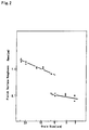
- Fig. 3 shows a relation between etching amount and surface condition factor(K) on the back surface of the substrate, and the surface condition factor corresponds to a bend degree of the wafer.
- the relation shown in Fig. 3 proves the etching amount is sufficient, because K value is restored to the same level as that of polished surface at 0.6 micro-meters etching (See "Technique of GaAs wafer mirror grinding" in Super-Precision Machining manual).
- a broken line shows polished surface, white dots non-mirror grinding (rough grinding) and filled dots mirror grinding respectively.
- the applicant measured "the Fracture Stress" of GaAs substrates respectively manufactured by the following two methods 1 and 2, by two different methods, one is a so-called “Four-Point Loading method” and the other is a so-called “Biaxial Loading method",
- Table I shows "Fracture Stress data” obtained by the Four-point Loading method and Table II shows “Fracture Stress data” obtained by the Biaxial Loading method.
- GaAs wafer is divided into individual IC chip by a dicing machine.
- the divided IC chip is die bonded on a ceramic plate by an eutectic alloy using AuSu etc.
- the back surface of the GaAs is metalized by Ti evaporation etc. and further Au layer is deposited thereon.
- a combination of the high speed grinding and the chemical etching enables a semiconductor element with sufficiently strong GaAs substrate to be manufactured in a short time of period.
- mirror grinding treatment can be eliminated, which simplifies manufacturing facilities and shortens manufacturing time. Consequently the present invention enables the semiconductor element to be manufactured at a low cost.
Landscapes
- Engineering & Computer Science (AREA)
- Microelectronics & Electronic Packaging (AREA)
- Condensed Matter Physics & Semiconductors (AREA)
- General Physics & Mathematics (AREA)
- Manufacturing & Machinery (AREA)
- Computer Hardware Design (AREA)
- Physics & Mathematics (AREA)
- Power Engineering (AREA)
- Chemical & Material Sciences (AREA)
- Chemical Kinetics & Catalysis (AREA)
- General Chemical & Material Sciences (AREA)
- Mechanical Treatment Of Semiconductor (AREA)
- Weting (AREA)
Abstract
Description
- The present invention relates to a method of manufacturing a semiconductor device and more particularly relates to a treatment of a back surface of a GaAs substrate on which a semiconductor device is formed.
- A semiconductor element formed on a GaAs Substrate, a chemical compound semiconductor, has a difficulty to dissipate heat generated from the device formed on a surface of the GaAs substrate, since thermal conductivity of GaAs is 1/3 times as low as that of Si. It adversely affects characteristics of the device. And, it is necessary to thin the substrate and assure a good dissipation of heat. On the other hand, GaAs is brittle compared with Si and easy to be cracked and/or broken off. So, chip cracking is easily caused starting from fine flaws and the like yielded at a thinning process. Therefore, mirror surface finish has been conventionally adopted with a grinding stone having fine grain sizes (See "THE IMPACT OF WAFER BACK SURFACE FINISH ON CHIP STRENGTH" of IEEE/IRPS). And, an application filed by the assignee and inventor of the present invention on Dec. 5, 1986 also disclosed that GaAs substrate has the maximum strength after die-bonding when back finish (R max) of the substrate is somewhat between 0.2 and 0.5 micro-meters. It is, however, difficult to obtain R max in this region only with grinding. And, in the prior art, mirror grinding has been used to obtain R max of 0.1 micro-meters or finer to eliminate fine flaws, consequently preventing a chip from being cracked.
- A grinding stone with fine grains, however, must be used to perform the aforementioned mirror grinding. It means only a small amount to be ground off per a unit time and taking a long time of period to grind off a predetermined amount. It results in low productivity for mass production and in making a process complicated because of a need of facilities for mirror grinding.
- In view of the above mentioned circumstances, it is an object of the present invention to provide a semiconductor device manufacturing process, wherein a back treatment can be performed in a short time of period and also semiconductor device can be manufactured with minimum chip cracking.
- Accordingly, the present invention provides a method of manufacturing a semiconductor device comprising the steps of: forming a semiconductor element on one of major surfaces of a GaAs substrate; a grinding the substrate to make the GaAs substrate to a predetermined thickness by grinding the other surface of the GaAs substrate with a grinding stone having an average grain size of 6 micro-meters or larger; and an chemical etching the other surface of the substrate by 0.6 micro-meters or more just after the grinding step, without any further grinding treatment done on the other surface, just after the grinding step.
- In a method according to the present invention, a grinding stone with a grain size of 6 micro-meters or larger is used to grind a GaAs substrate, on which a semiconductor element is formed, in a short time of period. And thereafter a chemical etching removes a deformed layer on a back surface of the substrate caused by the above mentioned grinding step. It enables to manufacture a GaAs substrate with high strength, in a short time of period.
- The present invention will become more fully understood from the detailed description given hereinbelow and the accompanying drawings which are given by way of illustration only, and thus are not to be considered as limiting the present invention.
- Further scope of applicability of the present invention will become apparent from the detailed description given hereinafter. However, it should be understood that the detailed description and specific examples, while indicating preferred embodiments of the invention, are given by way of illustration only, since various changes and modifications within the spirit and scope of the invention will become apparent to those skilled in the art form this detailed description.
-
- Fig. 1 shows a summarized flow chart of characterizing portions of an embodiment according to the present invention;
- Fig. 2 is a graph showing relation between grain size of grinding stone and finish surface roughness R max; and
- Fig. 3 is a graph showing relation between amount of etching and surface condition factor K of the back surface of GaAs substrate.
- Referring to Drawings, an embodiment according to the present invention is explained as follows.
- As shown in Fig. 1, the characterizing process is comprised of step 1 of forming a semiconductor element on a surface of the GaAs substrate,
step 2 of grinding off a back side of the GaAs substrate on which the semiconductor element is formed, and a step 3 of performing chemical etching to remove the back side by a predetermined thickness, just after the grinding step. - Concretely, a semiconductor element is formed on one of main surfaces of the GaAs wafer first. The semiconductor element is, for example Shottky-gate type field effect transistor or the like and on the one main surface, monolithic microwave integrated circuit or the like is formed by such field effect transistors. This step is performed utilizing photo-lithograph technique, ion implantation technique and the like. These are not described in detail here, as conventionally well known.
- Secondly, the one surface of the GaAs wafer on which the semiconductor element is formed is completely covered with a film made of organic material etc. and thereafter the wafer is mounted on a grinding machine by holding the covered surface thereof on a rotational stage of the grinding machine to grind the back side surface of the wafer. In the grinding, that is a so called a back grinding, the rotational stage mounting the wafer thereon is rotated and forwarded to a grinding stone rotating and located so as to face to the rotational stage and as the result the back side of the wafer is made in contact with the grinding stone to be ground. Usually, a wafer rotation down-feed method is used, as grinding resistance can be kept constant in it. And a diamond grinding stone with an average grain size of 6 micro-meters or larger is used. The reason why the average grain size of 6 or larger is adopted is that grinding speed would drastically decrease with a smaller grain size because the finish must be of mirror grinding. And, in case of the average grain size of 6 micro-meters or larger, surface finish roughness (R max) falls under approximately 1. This roughness enables the surface to be finished to nearly a desired value (0.2 to 0.5 micro-meters) with the chemical etching treatment following the prior grinding treatment. Fig.2 shows a relation between an average grain of a diamond grinding stone (horizontal axis) and a roughness (R max) (vertical axis) in the surface to be finished. As shown in Fig. 2, when the average grain changes from 6 micro-meters to 25 micro-meters, in response to the change, the roughness changes from 0.7 micro-meters to 3 micro-meters. Further in about 6 micro-meters of the average grain, the amount of R max changes incontinuously. This shows that 6 micro-meters in a size of the average grain is critical value. Generally, such incontinuous change in R max can not be observed in the grinding in Si wafer and such incontinuous change was also observed by a scanning electron microscope.
- Next, the back surface of the wafer is chemically etched without any further grinding treatment. In the chemical etching step 3, the side of the GaAs substrate on which the semiconductor element is formed is covered with a protection film, before the substrate is soaked in a mixture of ammonia, hydrogen dioxide and water. The mixture should have a very low etching speed. An example of the mixing ratio of such a mixture is NH₄OH : H₂O₂ : H₂O = 1 : 1 : 10, and the substrate is soaked in it for about 20 seconds. Various liquid mixture can be used as an etchant, for example, phosphoric based etchant, potassium-hydroxide based etchant or aqua regia etc. The step chemically etches the back surface of the GaAs wafer by 0.6 micro-meters or more.
- The amount of etching should be 0.6 micron-meters or more because the thickness of the deformed layer yielded on the back surface of the GaAs wafer by the previous grinding is about 0.6 micro-meters. A bend or the like in the wafer can be satisfactorily removed only by removing the deformed layer. Fig. 3 shows a relation between etching amount and surface condition factor(K) on the back surface of the substrate, and the surface condition factor corresponds to a bend degree of the wafer. The relation shown in Fig. 3 proves the etching amount is sufficient, because K value is restored to the same level as that of polished surface at 0.6 micro-meters etching (See "Technique of GaAs wafer mirror grinding" in Super-Precision Machining manual). In Fig.3, a broken line shows polished surface, white dots non-mirror grinding (rough grinding) and filled dots mirror grinding respectively.
- Semiconductor elements were manufactured by the above method and the Die-Shear Strength was compared between following two cases:
- (1) mirror grinding the back surface of the wafer to make R max to be 0.1 micro-meters and thereafter etching it by 0.1 micro-meters; and
- (2) rough grinding the back surface of the wafer to make R max to be 1 micro-meter and thereafter etching it by 0.6 micro-meters.
- And it was observed that the strength was 1.5 kg/mm in the both cases. In addition, no cracking was caused in a 5 x 5mm chip by 1000 cycle thermal impact of -65°C to +150°C, with 0.6 micro-meter etching even in case that R max was 1 micro-meter.
- Further, the applicant (inventor) measured "the Fracture Stress" of GaAs substrates respectively manufactured by the following two
methods 1 and 2, by two different methods, one is a so-called "Four-Point Loading method" and the other is a so-called "Biaxial Loading method", - (1) Method 1, Which is corresponding to a conventional method: Rough-grinding, Mirror-grinding and chemical etching are applied to a back surface of the substrate.
- (2)
Method 2, Which is corresponding to a method according to the present invention; - Rough grinding and chemical etching are applied to a back surface of the substrate without the application of Mirror grinding. Table I shows "Fracture Stress data" obtained by the Four-point Loading method and Table II shows "Fracture Stress data" obtained by the Biaxial Loading method.
TABLE I FRACTURE STRESS DATA FOR FOUR-POINT LOADING Manufacturing method Thickness Mean Fracture Stress Weibull Modulus 1 450 µm 163 2.2 1 300 µm 156 3.6 1 200 µm 181 2.4 2 450 µm 182 3.3 2 300 µm 173 3.4 2 200 µm 163 7.3 2 140 µm 154 2.1 TABLE II FRACTURE STRESS DATA FOR BIAXIAL LOADING Manufacturing method Thickness Mean Fracture Stress Weibull Modulus 1 450 µm 187 3.1 1 300 µm 179 2.5 1 200 µm 199 1.9 2 450 µm 129 5.5 2 300 µm 110 9.9 2 200 µm 102 5.8 2 140 µm 114 6.4 - The above results shown in the tables I and II was published in a paper titled as "High Mechanical Reliability of Back-ground GaAs LSI Chips with Low Thermal Resistance" on pages 890 to 896 in Proceedings of the 41st Electronic Components and Technology Conference (ECTC) held on May 13 to 15, 1991 at Atlanta in U.S.A., by the applicant (inventor) the present invention.
- As shown in the tables I and II, Fracture Stress data of the substrates manufactured by the two
method 1 and 2 are substantial equal to each other. Therefore, it can be understood that the substrate manufactured by themethod 2 has the substantially same strength as that of the substrate manufactured by themethod 2. - After the above chemical etching, GaAs wafer is divided into individual IC chip by a dicing machine. The divided IC chip is die bonded on a ceramic plate by an eutectic alloy using AuSu etc. Besides, before the die bonding, the back surface of the GaAs is metalized by Ti evaporation etc. and further Au layer is deposited thereon.
- As described above, according to the present invention, a combination of the high speed grinding and the chemical etching enables a semiconductor element with sufficiently strong GaAs substrate to be manufactured in a short time of period.
- Additionally, mirror grinding treatment can be eliminated, which simplifies manufacturing facilities and shortens manufacturing time. Consequently the present invention enables the semiconductor element to be manufactured at a low cost.
- From the invention thus described, it will be obvious that the invention may be varied in many ways. Such variations are not to be regarded as a departure from the spirit and scope of the invention, and all such modifications as would be obvious to one skilled in the art are intended to be included within the scope of the following claims.
Claims (3)
- A method of manufacturing a semiconductor device comprising the steps of:- forming a semiconductor element on one of major surfaces of a GaAs substrate;- grinding the other surface of the GaAs substrate with a grinding stone having an average grain size of about 6 µm or larger to make the GaAs substrate to a predetermined thickness; and- chemical etching the other surface of the substrate by 0.6 µm or more just after the grinding step, without any further grinding treatment done on this other surface.
- The method according to claim 1, wherein said grinding stone is a diamond grinding stone.
- The method according to claim 2, wherein said diamond grinding stone has an average grain size larger than 6 µm and smaller than 25 µm.
Applications Claiming Priority (2)
| Application Number | Priority Date | Filing Date | Title |
|---|---|---|---|
| JP2235152A JP2610703B2 (en) | 1990-09-05 | 1990-09-05 | Method for manufacturing semiconductor device |
| JP235152/90 | 1990-09-05 |
Publications (3)
| Publication Number | Publication Date |
|---|---|
| EP0475259A2 true EP0475259A2 (en) | 1992-03-18 |
| EP0475259A3 EP0475259A3 (en) | 1992-12-16 |
| EP0475259B1 EP0475259B1 (en) | 1995-08-30 |
Family
ID=16981823
Family Applications (1)
| Application Number | Title | Priority Date | Filing Date |
|---|---|---|---|
| EP91114907A Expired - Lifetime EP0475259B1 (en) | 1990-09-05 | 1991-09-04 | Semiconductor element manufacturing process |
Country Status (8)
| Country | Link |
|---|---|
| US (1) | US5122481A (en) |
| EP (1) | EP0475259B1 (en) |
| JP (1) | JP2610703B2 (en) |
| KR (1) | KR940002915B1 (en) |
| AU (1) | AU649063B2 (en) |
| CA (1) | CA2050675A1 (en) |
| DE (1) | DE69112545T2 (en) |
| DK (1) | DK0475259T3 (en) |
Cited By (5)
| Publication number | Priority date | Publication date | Assignee | Title |
|---|---|---|---|---|
| EP0603514A2 (en) * | 1992-12-21 | 1994-06-29 | Motorola, Inc. | Method for thinning a semiconductor wafer |
| EP0676717A2 (en) * | 1994-04-11 | 1995-10-11 | AT&T Corp. | Thin, strong and flexible die for smart cards |
| WO2000068990A1 (en) * | 1999-05-07 | 2000-11-16 | Giesecke & Devrient Gmbh | Method for handling thinned chips for introducing them into chip cards |
| EP1453090A2 (en) * | 2003-02-25 | 2004-09-01 | Sanyo Electric Co., Ltd. | Manufacturing method of semiconductor device |
| GB2459301A (en) * | 2008-04-18 | 2009-10-21 | Xsil Technology Ltd | A method of dicing wafers to give high die strength |
Families Citing this family (15)
| Publication number | Priority date | Publication date | Assignee | Title |
|---|---|---|---|---|
| US5279704A (en) * | 1991-04-23 | 1994-01-18 | Honda Giken Kogyo Kabushiki Kaisha | Method of fabricating semiconductor device |
| US5245794A (en) * | 1992-04-09 | 1993-09-21 | Advanced Micro Devices, Inc. | Audio end point detector for chemical-mechanical polishing and method therefor |
| JPH0817777A (en) * | 1994-07-01 | 1996-01-19 | Mitsubishi Materials Shilicon Corp | Method for washing silicon wafer |
| US5691248A (en) * | 1995-07-26 | 1997-11-25 | International Business Machines Corporation | Methods for precise definition of integrated circuit chip edges |
| US5648684A (en) * | 1995-07-26 | 1997-07-15 | International Business Machines Corporation | Endcap chip with conductive, monolithic L-connect for multichip stack |
| US6059637A (en) * | 1997-12-15 | 2000-05-09 | Lsi Logic Corporation | Process for abrasive removal of copper from the back surface of a silicon substrate |
| US6560871B1 (en) * | 2000-03-21 | 2003-05-13 | Hewlett-Packard Development Company, L.P. | Semiconductor substrate having increased facture strength and method of forming the same |
| US6520844B2 (en) * | 2000-08-04 | 2003-02-18 | Sharp Kabushiki Kaisha | Method of thinning semiconductor wafer capable of preventing its front from being contaminated and back grinding device for semiconductor wafers |
| ATE534142T1 (en) | 2002-03-12 | 2011-12-15 | Hamamatsu Photonics Kk | METHOD FOR SEPARATING A SUBSTRATE |
| JP2005005380A (en) * | 2003-06-10 | 2005-01-06 | Sanyo Electric Co Ltd | Method of manufacturing semiconductor device |
| JP2005026314A (en) * | 2003-06-30 | 2005-01-27 | Sanyo Electric Co Ltd | Method of manufacturing solid-state imaging device |
| JP2005303218A (en) * | 2004-04-16 | 2005-10-27 | Renesas Technology Corp | Semiconductor device and its manufacturing method |
| JP4872208B2 (en) * | 2004-11-18 | 2012-02-08 | 富士電機株式会社 | Manufacturing method of semiconductor device |
| JP5149020B2 (en) * | 2008-01-23 | 2013-02-20 | 株式会社ディスコ | Wafer grinding method |
| KR20230108142A (en) * | 2022-01-10 | 2023-07-18 | 도레이첨단소재 주식회사 | High tensile meta-aramid fiber and manufacturing method thereof |
Family Cites Families (9)
| Publication number | Priority date | Publication date | Assignee | Title |
|---|---|---|---|---|
| SU393073A1 (en) * | 1970-12-04 | 1973-08-10 | THE METHOD OF INCREASING THE DURABILITY OF DIAMOND, FOR EXAMPLE, ANIMAL TOOLING INSTRUMENTS | |
| AU527845B2 (en) * | 1978-01-19 | 1983-03-24 | E. Sachs & Co. Ltd | Fascia gutter |
| US4411107A (en) * | 1980-02-01 | 1983-10-25 | Disco Co., Ltd. | Grinding wheel for flat plates |
| FR2505713A1 (en) * | 1981-05-18 | 1982-11-19 | Procedes Equip Sciences Ind Sa | Semiconductor wafer carrying head for polishing machine - has circular disc covered in thin tissue with reduced pressure behind tissue to hold wafers |
| DE3148957A1 (en) * | 1981-12-10 | 1983-06-23 | Wacker-Chemitronic Gesellschaft für Elektronik-Grundstoffe mbH, 8263 Burghausen | "METHOD FOR THE BACK-SIDING SURFACE TREATMENT OF SEMICONDUCTOR DISC" |
| JPS58184727A (en) * | 1982-04-23 | 1983-10-28 | Disco Abrasive Sys Ltd | Processing apparatus for semiconductor material and satin-finished surface thereof |
| JPS62243332A (en) * | 1986-04-15 | 1987-10-23 | Toshiba Corp | Processing of semiconductor wafer |
| EP0272531B1 (en) * | 1986-12-08 | 1991-07-31 | Sumitomo Electric Industries Limited | Surface grinding machine |
| JPS6437025A (en) * | 1987-08-03 | 1989-02-07 | Sumitomo Electric Industries | Manufacture of semiconductor device |
-
1990
- 1990-09-05 JP JP2235152A patent/JP2610703B2/en not_active Expired - Lifetime
-
1991
- 1991-08-20 KR KR1019910014294A patent/KR940002915B1/en not_active IP Right Cessation
- 1991-09-03 AU AU83538/91A patent/AU649063B2/en not_active Ceased
- 1991-09-04 CA CA002050675A patent/CA2050675A1/en not_active Abandoned
- 1991-09-04 DE DE69112545T patent/DE69112545T2/en not_active Expired - Fee Related
- 1991-09-04 US US07/754,906 patent/US5122481A/en not_active Expired - Lifetime
- 1991-09-04 DK DK91114907.8T patent/DK0475259T3/en active
- 1991-09-04 EP EP91114907A patent/EP0475259B1/en not_active Expired - Lifetime
Non-Patent Citations (2)
| Title |
|---|
| IEEE TRANSACTIONS ON COMPONENTS,HYBRIDS,AND MANUFACTURING vol. 13, no. 3, 1 September 1990, NEW YORK US pages 528 - 533 M. NISHIGUCHI ET AL 'Mass Production Back-Grinding/Wafer Thinning Technology for GaAs Devices' * |
| PROCEEDINGS OF THE ELECTRONIC COMPONENTS AND TECHNOLOGY CONFERENCE. vol. 41, 11 May 1991, ATLANTA (US) pages 890 - 896 M. NISHIGUCHI ET AL 'High Mechanical Reliability Of Back-Ground GaAs LSI Chips with Low Thermal Resistance' * |
Cited By (11)
| Publication number | Priority date | Publication date | Assignee | Title |
|---|---|---|---|---|
| EP0603514A2 (en) * | 1992-12-21 | 1994-06-29 | Motorola, Inc. | Method for thinning a semiconductor wafer |
| EP0603514A3 (en) * | 1992-12-21 | 1995-07-26 | Motorola Inc | Method for thinning a semiconductor wafer. |
| EP0676717A2 (en) * | 1994-04-11 | 1995-10-11 | AT&T Corp. | Thin, strong and flexible die for smart cards |
| EP0676717A3 (en) * | 1994-04-11 | 1997-06-04 | At & T Corp | Thin, strong and flexible die for smart cards. |
| WO2000068990A1 (en) * | 1999-05-07 | 2000-11-16 | Giesecke & Devrient Gmbh | Method for handling thinned chips for introducing them into chip cards |
| DE19921230B4 (en) * | 1999-05-07 | 2009-04-02 | Giesecke & Devrient Gmbh | Method for handling thinned chips for insertion in chip cards |
| EP1453090A2 (en) * | 2003-02-25 | 2004-09-01 | Sanyo Electric Co., Ltd. | Manufacturing method of semiconductor device |
| EP1453090A3 (en) * | 2003-02-25 | 2008-06-04 | Sanyo Electric Co., Ltd. | Manufacturing method of semiconductor device |
| US7981807B2 (en) | 2003-02-25 | 2011-07-19 | Sanyo Electric Co., Ltd. | Manufacturing method of semiconductor device with smoothing |
| GB2459301A (en) * | 2008-04-18 | 2009-10-21 | Xsil Technology Ltd | A method of dicing wafers to give high die strength |
| GB2459301B (en) * | 2008-04-18 | 2011-09-14 | Xsil Technology Ltd | A method of dicing wafers to give high die strength |
Also Published As
| Publication number | Publication date |
|---|---|
| JP2610703B2 (en) | 1997-05-14 |
| KR940002915B1 (en) | 1994-04-07 |
| DE69112545T2 (en) | 1996-05-02 |
| EP0475259A3 (en) | 1992-12-16 |
| EP0475259B1 (en) | 1995-08-30 |
| AU8353891A (en) | 1992-03-12 |
| CA2050675A1 (en) | 1992-03-06 |
| KR920007104A (en) | 1992-04-28 |
| US5122481A (en) | 1992-06-16 |
| AU649063B2 (en) | 1994-05-12 |
| DK0475259T3 (en) | 1996-01-15 |
| JPH04115528A (en) | 1992-04-16 |
| DE69112545D1 (en) | 1995-10-05 |
Similar Documents
| Publication | Publication Date | Title |
|---|---|---|
| US5122481A (en) | Semiconductor element manufacturing process using sequential grinding and chemical etching steps | |
| US7427811B2 (en) | Semiconductor substrate | |
| US6245677B1 (en) | Backside chemical etching and polishing | |
| KR100589570B1 (en) | Method for manufacturing semiconductor device | |
| US6214704B1 (en) | Method of processing semiconductor wafers to build in back surface damage | |
| US5851924A (en) | Method for fabricating semiconductor wafers | |
| US7989358B2 (en) | Prevention of backside cracks in semiconductor chips or wafers using backside film or backside wet etch | |
| US6872598B2 (en) | Method of making a thin semiconductor chip | |
| US6750082B2 (en) | Method of assembling a package with an exposed die backside with and without a heatsink for flip-chip | |
| US6017822A (en) | Method of thinning semiconductor wafer of smaller diameter than thinning equipment was designed for | |
| JP2000294522A (en) | Dividing method of wafer and manufacture of semiconductor device | |
| US7498236B2 (en) | Silicon wafer thinning end point method | |
| US5849636A (en) | Method for fabricating a semiconductor wafer | |
| JP2588326B2 (en) | Method for manufacturing semiconductor wafer | |
| JP3803214B2 (en) | Manufacturing method of semiconductor device | |
| JP3179970B2 (en) | Resin-sealed semiconductor device and method of manufacturing the same | |
| US7504337B2 (en) | IC chip uniform delayering methods | |
| JPH0837169A (en) | Method and apparatus for grinding semiconductor substrate and manufacture of semiconductor device | |
| JP2000340530A (en) | Semiconductor device and manufacture thereof | |
| CN113053798A (en) | Ultrathin crystal thinning and cutting process utilizing tempered glass | |
| JP2001085285A (en) | Semiconductor device and its manufacture | |
| US6894389B2 (en) | Semiconductor device and manufacturing method therefor | |
| KR20060085848A (en) | Method of fabricating semiconductor wafer having bump forming process after back grinding | |
| JP2001071244A (en) | Precise chamfering method for semiconductor wafer | |
| JP2001297957A (en) | Compound semiconductor wafer |
Legal Events
| Date | Code | Title | Description |
|---|---|---|---|
| PUAI | Public reference made under article 153(3) epc to a published international application that has entered the european phase |
Free format text: ORIGINAL CODE: 0009012 |
|
| AK | Designated contracting states |
Kind code of ref document: A2 Designated state(s): DE DK FR GB IT NL |
|
| PUAL | Search report despatched |
Free format text: ORIGINAL CODE: 0009013 |
|
| AK | Designated contracting states |
Kind code of ref document: A3 Designated state(s): DE DK FR GB IT NL |
|
| 17P | Request for examination filed |
Effective date: 19930615 |
|
| 17Q | First examination report despatched |
Effective date: 19941019 |
|
| GRAA | (expected) grant |
Free format text: ORIGINAL CODE: 0009210 |
|
| AK | Designated contracting states |
Kind code of ref document: B1 Designated state(s): DE DK FR GB IT NL |
|
| REF | Corresponds to: |
Ref document number: 69112545 Country of ref document: DE Date of ref document: 19951005 |
|
| ITF | It: translation for a ep patent filed |
Owner name: ING. C. GREGORJ S.P.A. |
|
| ET | Fr: translation filed | ||
| REG | Reference to a national code |
Ref country code: DK Ref legal event code: T3 |
|
| PLBE | No opposition filed within time limit |
Free format text: ORIGINAL CODE: 0009261 |
|
| STAA | Information on the status of an ep patent application or granted ep patent |
Free format text: STATUS: NO OPPOSITION FILED WITHIN TIME LIMIT |
|
| 26N | No opposition filed | ||
| REG | Reference to a national code |
Ref country code: GB Ref legal event code: IF02 |
|
| PGFP | Annual fee paid to national office [announced via postgrant information from national office to epo] |
Ref country code: GB Payment date: 20040901 Year of fee payment: 14 |
|
| PGFP | Annual fee paid to national office [announced via postgrant information from national office to epo] |
Ref country code: DE Payment date: 20040902 Year of fee payment: 14 |
|
| PGFP | Annual fee paid to national office [announced via postgrant information from national office to epo] |
Ref country code: NL Payment date: 20040905 Year of fee payment: 14 |
|
| PGFP | Annual fee paid to national office [announced via postgrant information from national office to epo] |
Ref country code: FR Payment date: 20040908 Year of fee payment: 14 |
|
| PGFP | Annual fee paid to national office [announced via postgrant information from national office to epo] |
Ref country code: DK Payment date: 20040916 Year of fee payment: 14 |
|
| PG25 | Lapsed in a contracting state [announced via postgrant information from national office to epo] |
Ref country code: IT Free format text: LAPSE BECAUSE OF NON-PAYMENT OF DUE FEES;WARNING: LAPSES OF ITALIAN PATENTS WITH EFFECTIVE DATE BEFORE 2007 MAY HAVE OCCURRED AT ANY TIME BEFORE 2007. THE CORRECT EFFECTIVE DATE MAY BE DIFFERENT FROM THE ONE RECORDED. Effective date: 20050904 Ref country code: GB Free format text: LAPSE BECAUSE OF NON-PAYMENT OF DUE FEES Effective date: 20050904 |
|
| PG25 | Lapsed in a contracting state [announced via postgrant information from national office to epo] |
Ref country code: DK Free format text: LAPSE BECAUSE OF NON-PAYMENT OF DUE FEES Effective date: 20050930 |
|
| PG25 | Lapsed in a contracting state [announced via postgrant information from national office to epo] |
Ref country code: NL Free format text: LAPSE BECAUSE OF NON-PAYMENT OF DUE FEES Effective date: 20060401 Ref country code: DE Free format text: LAPSE BECAUSE OF NON-PAYMENT OF DUE FEES Effective date: 20060401 |
|
| REG | Reference to a national code |
Ref country code: DK Ref legal event code: EBP |
|
| GBPC | Gb: european patent ceased through non-payment of renewal fee |
Effective date: 20050904 |
|
| PG25 | Lapsed in a contracting state [announced via postgrant information from national office to epo] |
Ref country code: FR Free format text: LAPSE BECAUSE OF NON-PAYMENT OF DUE FEES Effective date: 20060531 |
|
| NLV4 | Nl: lapsed or anulled due to non-payment of the annual fee |
Effective date: 20060401 |
|
| REG | Reference to a national code |
Ref country code: FR Ref legal event code: ST Effective date: 20060531 |