EP0602579A1 - Halbleiterlaser und Herstellungsverfahren - Google Patents
Halbleiterlaser und Herstellungsverfahren Download PDFInfo
- Publication number
- EP0602579A1 EP0602579A1 EP93120076A EP93120076A EP0602579A1 EP 0602579 A1 EP0602579 A1 EP 0602579A1 EP 93120076 A EP93120076 A EP 93120076A EP 93120076 A EP93120076 A EP 93120076A EP 0602579 A1 EP0602579 A1 EP 0602579A1
- Authority
- EP
- European Patent Office
- Prior art keywords
- layers
- conductivity type
- semiconductor laser
- facets
- layer
- Prior art date
- Legal status (The legal status is an assumption and is not a legal conclusion. Google has not performed a legal analysis and makes no representation as to the accuracy of the status listed.)
- Granted
Links
- 239000004065 semiconductor Substances 0.000 title claims abstract description 87
- 238000004519 manufacturing process Methods 0.000 title claims description 12
- 239000000758 substrate Substances 0.000 claims abstract description 53
- 238000005253 cladding Methods 0.000 claims abstract description 40
- 238000000034 method Methods 0.000 claims abstract description 30
- 230000004888 barrier function Effects 0.000 claims abstract description 18
- 238000001451 molecular beam epitaxy Methods 0.000 claims abstract description 5
- 238000005229 chemical vapour deposition Methods 0.000 claims abstract description 4
- 239000002184 metal Substances 0.000 claims abstract description 4
- 239000000463 material Substances 0.000 claims description 12
- 238000005530 etching Methods 0.000 claims description 4
- 230000031700 light absorption Effects 0.000 abstract description 6
- 230000003287 optical effect Effects 0.000 abstract description 2
- 229910000980 Aluminium gallium arsenide Inorganic materials 0.000 description 7
- 229910001218 Gallium arsenide Inorganic materials 0.000 description 6
- 230000000903 blocking effect Effects 0.000 description 3
- VYPSYNLAJGMNEJ-UHFFFAOYSA-N Silicium dioxide Chemical compound O=[Si]=O VYPSYNLAJGMNEJ-UHFFFAOYSA-N 0.000 description 2
- 230000015572 biosynthetic process Effects 0.000 description 2
- 238000000151 deposition Methods 0.000 description 2
- 230000000694 effects Effects 0.000 description 2
- 238000007792 addition Methods 0.000 description 1
- 238000006243 chemical reaction Methods 0.000 description 1
- 229910052681 coesite Inorganic materials 0.000 description 1
- 230000001427 coherent effect Effects 0.000 description 1
- 229910052906 cristobalite Inorganic materials 0.000 description 1
- 230000007423 decrease Effects 0.000 description 1
- 230000002950 deficient Effects 0.000 description 1
- 230000008021 deposition Effects 0.000 description 1
- 239000012535 impurity Substances 0.000 description 1
- 239000011810 insulating material Substances 0.000 description 1
- 239000012212 insulator Substances 0.000 description 1
- 230000000873 masking effect Effects 0.000 description 1
- 238000012986 modification Methods 0.000 description 1
- 230000004048 modification Effects 0.000 description 1
- 230000010355 oscillation Effects 0.000 description 1
- 238000000206 photolithography Methods 0.000 description 1
- 239000000377 silicon dioxide Substances 0.000 description 1
- 235000012239 silicon dioxide Nutrition 0.000 description 1
- 229910052682 stishovite Inorganic materials 0.000 description 1
- 229910052905 tridymite Inorganic materials 0.000 description 1
- 239000012808 vapor phase Substances 0.000 description 1
Images


Classifications
-
- H—ELECTRICITY
- H01—ELECTRIC ELEMENTS
- H01S—DEVICES USING THE PROCESS OF LIGHT AMPLIFICATION BY STIMULATED EMISSION OF RADIATION [LASER] TO AMPLIFY OR GENERATE LIGHT; DEVICES USING STIMULATED EMISSION OF ELECTROMAGNETIC RADIATION IN WAVE RANGES OTHER THAN OPTICAL
- H01S5/00—Semiconductor lasers
- H01S5/10—Construction or shape of the optical resonator, e.g. extended or external cavity, coupled cavities, bent-guide, varying width, thickness or composition of the active region
- H01S5/16—Window-type lasers, i.e. with a region of non-absorbing material between the active region and the reflecting surface
-
- H—ELECTRICITY
- H01—ELECTRIC ELEMENTS
- H01S—DEVICES USING THE PROCESS OF LIGHT AMPLIFICATION BY STIMULATED EMISSION OF RADIATION [LASER] TO AMPLIFY OR GENERATE LIGHT; DEVICES USING STIMULATED EMISSION OF ELECTROMAGNETIC RADIATION IN WAVE RANGES OTHER THAN OPTICAL
- H01S5/00—Semiconductor lasers
- H01S5/02—Structural details or components not essential to laser action
- H01S5/026—Monolithically integrated components, e.g. waveguides, monitoring photo-detectors, drivers
-
- H—ELECTRICITY
- H01—ELECTRIC ELEMENTS
- H01S—DEVICES USING THE PROCESS OF LIGHT AMPLIFICATION BY STIMULATED EMISSION OF RADIATION [LASER] TO AMPLIFY OR GENERATE LIGHT; DEVICES USING STIMULATED EMISSION OF ELECTROMAGNETIC RADIATION IN WAVE RANGES OTHER THAN OPTICAL
- H01S5/00—Semiconductor lasers
- H01S5/20—Structure or shape of the semiconductor body to guide the optical wave ; Confining structures perpendicular to the optical axis, e.g. index or gain guiding, stripe geometry, broad area lasers, gain tailoring, transverse or lateral reflectors, special cladding structures, MQW barrier reflection layers
- H01S5/22—Structure or shape of the semiconductor body to guide the optical wave ; Confining structures perpendicular to the optical axis, e.g. index or gain guiding, stripe geometry, broad area lasers, gain tailoring, transverse or lateral reflectors, special cladding structures, MQW barrier reflection layers having a ridge or stripe structure
- H01S5/227—Buried mesa structure ; Striped active layer
- H01S5/2272—Buried mesa structure ; Striped active layer grown by a mask induced selective growth
-
- H—ELECTRICITY
- H01—ELECTRIC ELEMENTS
- H01S—DEVICES USING THE PROCESS OF LIGHT AMPLIFICATION BY STIMULATED EMISSION OF RADIATION [LASER] TO AMPLIFY OR GENERATE LIGHT; DEVICES USING STIMULATED EMISSION OF ELECTROMAGNETIC RADIATION IN WAVE RANGES OTHER THAN OPTICAL
- H01S5/00—Semiconductor lasers
- H01S5/30—Structure or shape of the active region; Materials used for the active region
- H01S5/34—Structure or shape of the active region; Materials used for the active region comprising quantum well or superlattice structures, e.g. single quantum well [SQW] lasers, multiple quantum well [MQW] lasers or graded index separate confinement heterostructure [GRINSCH] lasers
- H01S5/3428—Structure or shape of the active region; Materials used for the active region comprising quantum well or superlattice structures, e.g. single quantum well [SQW] lasers, multiple quantum well [MQW] lasers or graded index separate confinement heterostructure [GRINSCH] lasers layer orientation perpendicular to the substrate
Definitions
- the present invention relates to a semiconductor laser including a window structure at facets for producing high power output without catastrophic optical damage (COD) that is produced in a relatively simple process.
- COD catastrophic optical damage
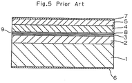
- Figure 5 is a cross-sectional view of a conventional semiconductor laser including an active layer with a multiple quantum well structure.
- That laser includes an n-type GaAs substrate 1 and a double heterojunction structure disposed on the substrate.
- the double heterojunction structure includes an n-type AlGaAs first cladding layer 2, an AlGaAs active layer 3 including a multiple quantum well structure, and a p-type AlGaAs second cladding layer 4.
- the semiconductor laser also includes a p-type GaAs contact layer 5 disposed on the second cladding layer 4 and electrodes 6 and 7 disposed on the substrate 1 and the contact layer 5, respectively.
- Opposed facets 8 and 9 of the semiconductor laser that form a resonator with the active layer and the first and second cladding layers are transverse to those layers.
- the active layer 3 includes alternatingly arranged well and barrier layers with relatively low and relatively high energy band gaps, respectively.
- the semiconductor laser When the semiconductor laser is forward biased, electrons and holes are injected into the active layer and recombine to produce light. When the current flowing between the electrodes exceeds a threshold current level, laser oscillation occurs and coherent light is produced by the laser. The light is emitted through one of the facets 8 and 9 that is coated with an imperfect reflector. Because of the reflection of the laser light within the active layer at the facets and the presence of surfaces states at the facets, during operation of the laser some of the light is absorbed at and adjacent the facets, locally increasing the temperature of the laser. If the temperature rises sufficiently, COD can occur in which semiconductor materials may begin to melt, destroying the semiconductor laser.
- window structures In order to increase the power output that a semiconductor laser can safely produce without COD, so-called window structures have been included in semiconductor lasers at the facets. Those window structures generally have an effective energy band gap larger than other parts of the active layer so that light is less easily absorbed at the facets than internally in the laser.
- a known technique for producing window structures includes disordering the multiple quantum well structure in the vicinity of the facets. When the multiple quantum well structure is disordered, the distinct boundaries between the well and barrier layers are blurred, resulting in a more homogeneous active layer at the facets. The more homogeneous material has a larger energy band gap than the effective energy band gap of the quantum well structure so that light absorption is reduced.
- Disordering may be produced thermally or by the introduction of impurities in controlled regions of the active layer adjacent the facets.
- impurities in controlled regions of the active layer adjacent the facets.
- a semiconductor laser comprises a semiconductor substrate of a first conductivity type; a first cladding layer of the first conductivity type, an active layer comprising a multiple quantum well structure including alternating well and barrier layers, and a second cladding layer of a second conductivity type, opposite the first conductivity type, successively disposed on the substrate; a contact layer of the second conductivity type disposed on the second cladding layer; and first and second electrodes respectively disposed on the substrate and the contact layer, the laser including opposed first and second facets transverse to the first and second cladding layers, wherein the well layers have a first thickness adjacent the first and second facets and a second thickness, greater than the first thickness, within the semiconductor laser intermediate the first and second facets.
- a method for producing a semiconductor laser comprises forming spaced apart insulating films on a semiconductor substrate of a first conductivity type defining a central groove and two regions transverse to, contiguous to, and continuous with the central groove, the semiconductor substrate being exposed in the groove and the two regions; successively, epitaxially growing a first cladding layer of a first conductivity type, an active layer comprising a multiple quantum well structure including alternating well and barrier layers, a second cladding layer of a second conductivity type, opposite the first conductivity type, and a contact layer of the second conductivity type on the semiconductor substrate using a process producing thicker well layers in the groove than in the two regions; and forming first and second electrodes on the substrate and the contact layer, respectively.
- a method for producing a semiconductor layer comprises forming a semiconductor substrate of a first conductivity type to include two opposed mesas separated by a central groove and adjacent two regions transverse to, contiguous to, and continuous with the central groove; successively, epitaxially growing a first cladding layer of a first conductivity type, an active layer comprising a multiple quantum well structure including alternating well and barrier layers, a second cladding layer of a second conductivity type, opposite the first conductivity type, and a contact layer of the second conductivity type on the semiconductor substrate using a process producing thicker well layers in the groove than in the two regions; and forming first and second electrodes on the substrate and the contact layer, respectively.
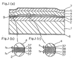
- Figure 1(a) is a cross-sectional view of a semiconductor laser in accordance with a first embodiment of the present invention.
- Figures 1(b) and 1(c) are enlarged partial views of parts of Figure 1(a).
- Figures 2(a)-2(c) are two perspective views and a sectional view illustrating a method of manufacturing the semiconductor laser of Figure 1(a).
- Figures 3(a)-3(c) are two perspective views and a sectional view illustrating a method of manufacturing the semiconductor laser of Figure 1(a).
- Figures 4(a)-4(c) are partial sectional views illustrating process steps that may be carried out subsequent to the step illustrated in Figure 3(c) in a method of making a semiconductor laser according to an embodiment of the invention.
- Figure 5 is a cross-sectional view of a prior art semiconductor laser.
- Figure 1(a) is a cross-sectional view of a semiconductor laser in accordance with an embodiment of the invention.
- the semiconductor laser of Figure 1(a) has a structure similar to the prior art semiconductor laser of Figure 5 except that the thickness of the active layer 3 varies.
- the active layer 3 is thinner adjacent the facets 8 and 9 than in the central parts of the semiconductor laser intermediate the facets 8 and 9.
- Figures 1(b) and 1(c) are enlarged detail views of the thinner and thicker parts of the active layer 3.
- Figure 1(b) the detailed structure of the multiple quantum well active layer 3 is shown. That structure includes well layers 38 that are sandwiched by barrier layers 37.
- the barrier layers 37 may be Al 0.2 Ga 0.8 As and have a thickness t3 of about 9 nanometers.
- the well layers 38 may be GaAs and have a thickness t4 of about 7.2 nanometers.
- the barrier layers 37 may have a thickness t1 of about 10 nanometers and the well layers may have a thickness t2 of about 8 nanometers.
- both the well layers and the barrier layers are about ten percent thinner in the vicinity of the facets 8 and 9 than in intermediate regions of the semiconductor laser remote from the facets.
- the fundamental operation of the semiconductor laser of Figure 1(a) is the same as that of the semiconductor laser of Figure 5.
- the novel semiconductor laser with the varying thickness active layer 3 if the well layers 38 are thinner than about 20 nanometers, the effective energy band gap of the multiple quantum well structure active layer 3 varies significantly with the thickness of the well layer due to quantum mechanical effects.
- the effective energy band gap of such a multiple quantum well structure increases as the thickness of the well layer decreases.
- the described multiple quantum well structure is symmetrical, i.e., has well layers of substantially the same thickness and barrier layers of substantially the same thickness.
- the invention is not limited to a perfectly symmetrical quantum well structure.
- the variations in the thicknesses of the well layers locally alter the effective energy band gap of the quantum well structure active layer.
- the energy band gap of the active layer 3 in the vicinity of the facets is larger than the energy band gap within the semiconductor laser.
- the larger energy band gap at the facets reduces light absorption so that the semiconductor laser according to the invention can be operated at a higher power than the prior art laser without risk of COD.
- the specific embodiment of the invention described above includes well and barrier layers of specific thicknesses and materials, other materials and thicknesses can be employed to produce the same effect providing the well layers are thinner in the vicinity of the laser facets than in the central portion of the laser structure. Since it is the thickness of the well layers that affects the effective energy band gap of the active layer 3, the barrier layers may have constant thicknesses throughout the active layer providing the well layers are thinner in the vicinity of the facets than elsewhere within the semiconductor laser.
- FIG. 2(a)-2(c) A method of making the semiconductor laser of Figure 1(a) is illustrated in Figures 2(a)-2(c).
- the n-type GaAs substrate 1 has masks 10a and 10b prepared on one of its surfaces for controlling epitaxial growth.
- the masks 10a and 10b are made of an insulator, such as SiO2 or SiN, about 100 nanometers thick. Other insulating materials may be used for the masks 10a and 10b as well.
- the unmasked portion of the substrate 1 resembles an upper case Roman letter I.
- the central part of the I is a stripe-shaped region or groove 11 that extends in what becomes the resonator length direction of the semiconductor laser.
- That groove 11 has a width W2, in one specific example of a semiconductor laser according to the invention, of 20 to 30 microns.
- the other parts of the letter I are the two regions 12 that are transverse to, contiguous to, and continuous with the groove 11.
- the two regions 12 are respectively disposed at what will become areas adjacent the two facets of the semiconductor laser.
- Those regions 12 have the full width of the substrate 1, W1, in this example about 300 microns.
- the length of those regions 12, L2, is about 10 to 20 microns.
- the overall length of the substrate, L1, in this example, is 300 to 500 microns.
- the representation in Figure 2(a) shows an isolated rectangular substrate 1, in practice, a plurality of semiconductor lasers are formed at the same time on a semiconductor wafer. Each semiconductor laser has a rectangular area defined on the wafer that corresponds to the substrate 1. Those rectangular areas may be adjacent and in contact with other, end-to-end and side-to-side.
- the n-type first cladding layer 2, the active layer 3, the second cladding layer 4, and the contact layer 5 are successively, epitaxially grown on the substrate 1.
- the epitaxial growth method chosen is one that results in the growth of crystalline semiconductor material preferentially on the semiconductor substrate 1 and not on the masks 10a and 10b.
- the species produced in a vapor phase reaction are highly mobile on the surfaces of the masks 10a and 10b but less mobile on the semiconductor substrate 1, resulting in preferential epitaxial growth on the substrate 1 and essentially no material deposition on the insulating film masks.
- Examples of such growth techniques are metal organic chemical vapor deposition (MOCVD) and molecular beam epitaxy (MBE).
- MOCVD metal organic chemical vapor deposition
- MBE molecular beam epitaxy
- Figure 2(c) is a cross-sectional view taken along line 2c-2c of Figure 2(b).
- Figure 2(c) is a cross-sectional view taken along line 2c-2c of Figure 2(b).
- the grown layers 2, 3, and 4 are thicker in the groove 11 than in the two transverse regions 12. Therefore, the first cladding layer 2, the well and barrier layers of the active layer 3, and the second cladding layer 4 are all thicker in the central region of the laser than adjacent the facets of the completed semiconductor laser. This result is achieved solely in the growth of the cladding and active layers. No additional process steps are required, as in the prior art, to form window regions by disordering a multiple quantum well structure active layer in the vicinity of the facets. Therefore, the window structures are produced simply and directly during the epitaxial growth process, improving the yield of the manufacturing process.
- a current confinement structure for concentrating current flow through the resonator section of the semiconductor laser is produced.
- One embodiment of a current confinement structure may be produced by controlling electrode geometry. Electrodes 6 and 7 are formed on the substrate 1 and the contact layer 5 of Figure 2(b), respectively. Then, the electrode 32 on the contact layer 5 is patterned to have a narrow stripe shape opposite the groove 11 and extending between the facets 8 and 9. That electrode geometry tends to direct the current flowing between the electrodes 6 and 7 to the part of the active layer 3 that is central along a direction transverse to the groove 11.
- a current confinement structure can include high resistivity or semi-insulating current blocking layers grown on opposite sides of and contacting the layers 2, 3, and 4, producing a buried heterojunction structure, for example, as described in more detail below with respect to Figures 4(b) and 4(c). If a current confinement structure is formed by growing or depositing high resistivity current blocking layers, after that step, the electrodes 6 and 7 are formed on the substrate 1 and the contact layer 5, respectively. If the electrode on the contact layer 5 is used as part of a current confinement structure, it is patterned. Subsequent to the formation of the electrodes 6 and 7, the facets 8 and 9 of the semiconductor laser are formed by cleaving, completing a semiconductor laser according to the invention.
- FIG. 3(a)-3(c) An alternative method of making the semiconductor laser of Figure 1(a) is illustrated in Figures 3(a)-3(c).
- the GaAs substrate 1 is shaped, for example, by masking and etching, to produce a structure having the same general shape as the substrate 1 of Figure 2(a) including the masks 10a and 10b.
- the substrate 1 of Figure 3(a) includes projecting mesas 14 and 15 defining a central groove 18 in which the resonator portion of the semiconductor laser will be formed by epitaxial growth. Two regions 19 at opposite ends of the substrate adjacent the mesas 14 and 15 are transverse to, contiguous to, and continuous with the central groove 18.
- the surface of the substrate 1 in the groove 18 and in the regions 19 lies in a single plane, as shown in Figure 3(a).
- the two regions 19 are at locations that will be adjacent the facets of the completed semiconductor laser.
- the regions 19 and the groove 18 are connected and again form the shape of the Roman letter I.
- the dimensions of the shaped substrate 1 of Figure 3(a) are essentially the same as those of the substrate 1 of Figure 2(a) except that the mesas 14 and 15 are about 5 microns in height as compared to the 100 nanometer thickness of the masks 10a and 10b of Figure 2(a).
- the first cladding layer 2, the active layer 3, the second cladding layer 4, and the contact layer 5 are successively grown by MOCVD or MBE, just as described with respect to Figure 2(b), to produce the structure shown in Figure 3(b).
- MOCVD or MBE MOCVD or MBE
- the difference in growth rates is not as large as in the embodiment of the invention described with respect to Figures 2(a) and 2(b).
- the same kind of structure is produced as a result of the epitaxial growth in both methods.
- the grown layers are thicker in the central portion of the semiconductor laser than adjacent the facets, producing the desired window structure as illustrated in the cross-sectional view of Figure 3(c) taken along line 3c-3c of Figure 3(b).
- Figures 4(a)-4(c) illustrate a process for forming a current confinement structure.
- Figure 4(a) is a cross-sectional view taken along line 4a-4a of Figure 3(b).
- a stripe-shaped etching mask 20, illustrated in Figure 4(b) is deposited on the contact layer 5 opposite the groove 18. Then, using the mask 20 to protect part of the grown layers, the laser structure is etched to remove the grown layers outside of the groove 18 and parts of the substrate 1 to produce the structure shown in Figure 4(b).
- a p-type AlGaAs layer 21, an n-type AlGaAs layer 22, and a p-type AlGaAs layer 23 are successively grown adjacent the mesa with the mask 20 in place to prevent the growth of semiconductor materials on the contact layer 5 at the top of the mesa.
- the mask 20 is subsequently removed and additional p-type GaAs is deposited as part of the contact layer 5 extending from the mesa across the p-type layer 23.
- the three grown layers 21-23, in combination with the contact layer 5 and the substrate 1 form a p-n-p-n current blocking structure.
- the semiconductor laser is completed by forming electrodes 6 and 7 on the contact layer and the substrate 1, respectively, followed by cleaving to produce the laser facets.
- the quantum well structure includes layers of AlGaAs.
- Other materials may be used for those layers and for the cladding layers, such as materials including AlInGaP.
Landscapes
- Physics & Mathematics (AREA)
- Condensed Matter Physics & Semiconductors (AREA)
- General Physics & Mathematics (AREA)
- Electromagnetism (AREA)
- Optics & Photonics (AREA)
- Semiconductor Lasers (AREA)
Applications Claiming Priority (2)
| Application Number | Priority Date | Filing Date | Title |
|---|---|---|---|
| JP4354578A JP2815769B2 (ja) | 1992-12-15 | 1992-12-15 | 半導体レーザの製造方法 |
| JP354578/92 | 1992-12-15 |
Publications (2)
| Publication Number | Publication Date |
|---|---|
| EP0602579A1 true EP0602579A1 (de) | 1994-06-22 |
| EP0602579B1 EP0602579B1 (de) | 1998-06-24 |
Family
ID=18438502
Family Applications (1)
| Application Number | Title | Priority Date | Filing Date |
|---|---|---|---|
| EP93120076A Expired - Lifetime EP0602579B1 (de) | 1992-12-15 | 1993-12-13 | Halbleiterlaser und Herstellungsverfahren |
Country Status (4)
| Country | Link |
|---|---|
| US (1) | US5486490A (de) |
| EP (1) | EP0602579B1 (de) |
| JP (1) | JP2815769B2 (de) |
| DE (1) | DE69319317T2 (de) |
Cited By (2)
| Publication number | Priority date | Publication date | Assignee | Title |
|---|---|---|---|---|
| WO1998021758A2 (de) * | 1996-11-08 | 1998-05-22 | Aventis Research & Technologies Gmbh & Co Kg | Elektrolumineszenzvorrichtung aus organischem material |
| EP1109231A2 (de) * | 1999-12-15 | 2001-06-20 | Matsushita Electronics Corporation | Lichtemittierende Halbleitervorrichtung und Herstellungsverfahren |
Families Citing this family (10)
| Publication number | Priority date | Publication date | Assignee | Title |
|---|---|---|---|---|
| JPH08307012A (ja) * | 1995-05-01 | 1996-11-22 | Mitsubishi Electric Corp | 選択成長用マスク,半導体光装置の製造方法,および半導体光装置 |
| JPH09128904A (ja) | 1995-11-01 | 1997-05-16 | Canon Inc | 情報再生装置 |
| US5757833A (en) * | 1995-11-06 | 1998-05-26 | The Furukawa Electric Co., Ltd. | Semiconductor laser having a transparent light emitting section, and a process of producing the same |
| JPH09252165A (ja) * | 1996-03-18 | 1997-09-22 | Fujitsu Ltd | 化合物半導体装置の製造方法 |
| US6267282B1 (en) * | 1999-04-01 | 2001-07-31 | Agere Systems Optoelectronics Guardian Corp. | Method and apparatus for handling laser bars |
| JP3804485B2 (ja) * | 2001-08-02 | 2006-08-02 | ソニー株式会社 | 半導体レーザー素子の製造方法 |
| US6898224B2 (en) * | 2001-08-22 | 2005-05-24 | The Furukawa Electric Co., Ltd. | Semiconductor laser device |
| KR100900471B1 (ko) * | 2004-01-29 | 2009-06-03 | 쇼와 덴코 가부시키가이샤 | 질화 갈륨계 화합물 반도체 다층 구조 및 그 제조방법 |
| DE102015104700A1 (de) * | 2015-03-27 | 2016-09-29 | Osram Opto Semiconductors Gmbh | Optoelektronischer Halbleiterchip |
| JP2017224763A (ja) * | 2016-06-16 | 2017-12-21 | 三菱電機株式会社 | 半導体素子の製造方法、半導体素子 |
Citations (6)
| Publication number | Priority date | Publication date | Assignee | Title |
|---|---|---|---|---|
| EP0081956A1 (de) * | 1981-12-03 | 1983-06-22 | Xerox Corporation | Injektionslaser mit integralem Wellenleiter |
| EP0264225A2 (de) * | 1986-10-07 | 1988-04-20 | Sharp Kabushiki Kaisha | Halbleiterlaservorrichtung und Verfahren zur Herstellung derselben |
| JPH01186693A (ja) * | 1988-01-14 | 1989-07-26 | Matsushita Electric Ind Co Ltd | 半導体装置およびその製造方法 |
| GB2237654A (en) * | 1989-11-02 | 1991-05-08 | Stc Plc | Semiconductor optical source |
| EP0472221A2 (de) * | 1990-08-24 | 1992-02-26 | Nec Corporation | Verfahren zur Herstellung einer optischen Halbleitervorrichtung |
| JPH04100291A (ja) * | 1990-08-20 | 1992-04-02 | Fujitsu Ltd | 半導体装置の製造方法および、光半導体装置の製造方法 |
Family Cites Families (4)
| Publication number | Priority date | Publication date | Assignee | Title |
|---|---|---|---|---|
| JPS6017979A (ja) * | 1983-07-11 | 1985-01-29 | Nec Corp | 半導体レ−ザ |
| JPH0314279A (ja) * | 1989-06-13 | 1991-01-22 | Matsushita Electric Ind Co Ltd | 半導体レーザ装置 |
| JPH0332084A (ja) * | 1989-06-29 | 1991-02-12 | Nec Corp | 半導体レーザの製造方法 |
| EP1186693B1 (de) * | 2000-09-04 | 2007-12-05 | Lg Electronics Inc. | Waschmachine und Verfahren zum ändern der Systemdaten in dieser Maschine |
-
1992
- 1992-12-15 JP JP4354578A patent/JP2815769B2/ja not_active Expired - Fee Related
-
1993
- 1993-12-13 DE DE69319317T patent/DE69319317T2/de not_active Expired - Fee Related
- 1993-12-13 EP EP93120076A patent/EP0602579B1/de not_active Expired - Lifetime
-
1994
- 1994-09-02 US US08/298,968 patent/US5486490A/en not_active Expired - Fee Related
Patent Citations (6)
| Publication number | Priority date | Publication date | Assignee | Title |
|---|---|---|---|---|
| EP0081956A1 (de) * | 1981-12-03 | 1983-06-22 | Xerox Corporation | Injektionslaser mit integralem Wellenleiter |
| EP0264225A2 (de) * | 1986-10-07 | 1988-04-20 | Sharp Kabushiki Kaisha | Halbleiterlaservorrichtung und Verfahren zur Herstellung derselben |
| JPH01186693A (ja) * | 1988-01-14 | 1989-07-26 | Matsushita Electric Ind Co Ltd | 半導体装置およびその製造方法 |
| GB2237654A (en) * | 1989-11-02 | 1991-05-08 | Stc Plc | Semiconductor optical source |
| JPH04100291A (ja) * | 1990-08-20 | 1992-04-02 | Fujitsu Ltd | 半導体装置の製造方法および、光半導体装置の製造方法 |
| EP0472221A2 (de) * | 1990-08-24 | 1992-02-26 | Nec Corporation | Verfahren zur Herstellung einer optischen Halbleitervorrichtung |
Non-Patent Citations (4)
| Title |
|---|
| A. SHIMA ET AL: "High power long cavity T3 laser with very narrow beam", JAPANESE JOURNAL OF APPLIED PHYSICS., vol. 28, no. 1, January 1989 (1989-01-01), TOKYO JP, pages L105 - L107, XP000111417, DOI: doi:10.1143/JJAP.28.L105 * |
| PATENT ABSTRACTS OF JAPAN vol. 13, no. 474 (E - 836) 26 October 1989 (1989-10-26) * |
| PATENT ABSTRACTS OF JAPAN vol. 16, no. 336 (E - 1237) 21 July 1992 (1992-07-21) * |
| R.D. BURNHAM ET AL: "Semiconductor injection lasers with quantum size effect transparant waveguiding", XEROX DISCLOSURE JOURNAL, vol. 11, no. 2, March 1986 (1986-03-01), STAMFORD, CONN US, pages 97 - 99 * |
Cited By (4)
| Publication number | Priority date | Publication date | Assignee | Title |
|---|---|---|---|---|
| WO1998021758A2 (de) * | 1996-11-08 | 1998-05-22 | Aventis Research & Technologies Gmbh & Co Kg | Elektrolumineszenzvorrichtung aus organischem material |
| WO1998021758A3 (de) * | 1996-11-08 | 1998-07-02 | Hoechst Res & Tech Gmbh & Co | Elektrolumineszenzvorrichtung aus organischem material |
| EP1109231A2 (de) * | 1999-12-15 | 2001-06-20 | Matsushita Electronics Corporation | Lichtemittierende Halbleitervorrichtung und Herstellungsverfahren |
| EP1109231A3 (de) * | 1999-12-15 | 2003-08-20 | Matsushita Electric Industrial Co., Ltd. | Lichtemittierende Halbleitervorrichtung und Herstellungsverfahren |
Also Published As
| Publication number | Publication date |
|---|---|
| JPH06181363A (ja) | 1994-06-28 |
| DE69319317D1 (de) | 1998-07-30 |
| EP0602579B1 (de) | 1998-06-24 |
| US5486490A (en) | 1996-01-23 |
| DE69319317T2 (de) | 1999-03-11 |
| JP2815769B2 (ja) | 1998-10-27 |
Similar Documents
| Publication | Publication Date | Title |
|---|---|---|
| KR100187778B1 (ko) | 매몰 헤테로 구조 레이저 및 그 제조 방법 | |
| EP0477013B1 (de) | Verfahren zur Herstellung eines Halbleiterlasers | |
| EP0663710A2 (de) | Optische Halbleitervorrichtung und Herstellungsverfahren | |
| US5737351A (en) | Semiconductor laser including ridge structure extending between window regions | |
| US5486490A (en) | Method of making semiconductor laser | |
| US5541950A (en) | Semiconductor laser including groove having variable dimensions | |
| EP0272096B1 (de) | Halbleiterlaser | |
| JPH0656906B2 (ja) | 半導体レ−ザ装置 | |
| US5115443A (en) | Semiconductor laser apparatus | |
| EP0157555B1 (de) | Halbleiterlaser und Verfahren zu dessen Fabrikation | |
| EP0488510B1 (de) | Oberflächenemittierender Laser für sichtbares Licht | |
| US5394421A (en) | Semiconductor laser device including a step electrode in a form of eaves | |
| EP0473443B1 (de) | Halbleiterlaser mit vergrabener Streifenstruktur | |
| US5870419A (en) | Double heterojunction semiconductor laser having improved light confinement | |
| EP0264225B1 (de) | Halbleiterlaservorrichtung und Verfahren zur Herstellung derselben | |
| EP0915542B1 (de) | Halbleiterlaser mit verbesserten stromsperrenden Schichten und Herstellungsverfahren | |
| US4841535A (en) | Semiconductor laser device | |
| US5887011A (en) | Semiconductor laser | |
| US5490159A (en) | Visible light semiconductor laser | |
| US5360763A (en) | Method for fabricating an optical semiconductor device | |
| JPH11150320A (ja) | 半導体発光装置とその製造方法 | |
| JP2550725B2 (ja) | 半導体レーザとその製造方法 | |
| JPH06260715A (ja) | 半導体レーザ素子およびその製造方法 | |
| JP2973215B2 (ja) | 半導体レーザ装置 | |
| JPH11354880A (ja) | 半導体レーザ素子およびその製造方法 |
Legal Events
| Date | Code | Title | Description |
|---|---|---|---|
| PUAI | Public reference made under article 153(3) epc to a published international application that has entered the european phase |
Free format text: ORIGINAL CODE: 0009012 |
|
| AK | Designated contracting states |
Kind code of ref document: A1 Designated state(s): DE FR GB NL |
|
| 17P | Request for examination filed |
Effective date: 19941007 |
|
| 17Q | First examination report despatched |
Effective date: 19960125 |
|
| GRAG | Despatch of communication of intention to grant |
Free format text: ORIGINAL CODE: EPIDOS AGRA |
|
| GRAG | Despatch of communication of intention to grant |
Free format text: ORIGINAL CODE: EPIDOS AGRA |
|
| GRAH | Despatch of communication of intention to grant a patent |
Free format text: ORIGINAL CODE: EPIDOS IGRA |
|
| GRAH | Despatch of communication of intention to grant a patent |
Free format text: ORIGINAL CODE: EPIDOS IGRA |
|
| GRAA | (expected) grant |
Free format text: ORIGINAL CODE: 0009210 |
|
| AK | Designated contracting states |
Kind code of ref document: B1 Designated state(s): DE FR GB NL |
|
| REF | Corresponds to: |
Ref document number: 69319317 Country of ref document: DE Date of ref document: 19980730 |
|
| ET | Fr: translation filed | ||
| PLBE | No opposition filed within time limit |
Free format text: ORIGINAL CODE: 0009261 |
|
| STAA | Information on the status of an ep patent application or granted ep patent |
Free format text: STATUS: NO OPPOSITION FILED WITHIN TIME LIMIT |
|
| 26N | No opposition filed | ||
| REG | Reference to a national code |
Ref country code: GB Ref legal event code: 727 |
|
| REG | Reference to a national code |
Ref country code: GB Ref legal event code: 727A |
|
| REG | Reference to a national code |
Ref country code: GB Ref legal event code: 727B |
|
| REG | Reference to a national code |
Ref country code: GB Ref legal event code: SP |
|
| REG | Reference to a national code |
Ref country code: GB Ref legal event code: IF02 |
|
| PGFP | Annual fee paid to national office [announced via postgrant information from national office to epo] |
Ref country code: NL Payment date: 20031205 Year of fee payment: 11 |
|
| PGFP | Annual fee paid to national office [announced via postgrant information from national office to epo] |
Ref country code: GB Payment date: 20031210 Year of fee payment: 11 Ref country code: FR Payment date: 20031210 Year of fee payment: 11 |
|
| PGFP | Annual fee paid to national office [announced via postgrant information from national office to epo] |
Ref country code: DE Payment date: 20031229 Year of fee payment: 11 |
|
| PG25 | Lapsed in a contracting state [announced via postgrant information from national office to epo] |
Ref country code: GB Free format text: LAPSE BECAUSE OF NON-PAYMENT OF DUE FEES Effective date: 20041213 |
|
| PG25 | Lapsed in a contracting state [announced via postgrant information from national office to epo] |
Ref country code: NL Free format text: LAPSE BECAUSE OF NON-PAYMENT OF DUE FEES Effective date: 20050701 Ref country code: DE Free format text: LAPSE BECAUSE OF NON-PAYMENT OF DUE FEES Effective date: 20050701 |
|
| GBPC | Gb: european patent ceased through non-payment of renewal fee |
Effective date: 20041213 |
|
| PG25 | Lapsed in a contracting state [announced via postgrant information from national office to epo] |
Ref country code: FR Free format text: LAPSE BECAUSE OF NON-PAYMENT OF DUE FEES Effective date: 20050831 |
|
| NLV4 | Nl: lapsed or anulled due to non-payment of the annual fee |
Effective date: 20050701 |
|
| REG | Reference to a national code |
Ref country code: FR Ref legal event code: ST |