EP0594413B1 - Modulator mit Kontrolle einer laufenden Digitalsumme - Google Patents
Modulator mit Kontrolle einer laufenden Digitalsumme Download PDFInfo
- Publication number
- EP0594413B1 EP0594413B1 EP93308352A EP93308352A EP0594413B1 EP 0594413 B1 EP0594413 B1 EP 0594413B1 EP 93308352 A EP93308352 A EP 93308352A EP 93308352 A EP93308352 A EP 93308352A EP 0594413 B1 EP0594413 B1 EP 0594413B1
- Authority
- EP
- European Patent Office
- Prior art keywords
- dsv
- margin
- bit
- signal
- margin bit
- Prior art date
- Legal status (The legal status is an assumption and is not a legal conclusion. Google has not performed a legal analysis and makes no representation as to the accuracy of the status listed.)
- Expired - Lifetime
Links
Images


Classifications
-
- G—PHYSICS
- G11—INFORMATION STORAGE
- G11B—INFORMATION STORAGE BASED ON RELATIVE MOVEMENT BETWEEN RECORD CARRIER AND TRANSDUCER
- G11B20/00—Signal processing not specific to the method of recording or reproducing; Circuits therefor
- G11B20/10—Digital recording or reproducing
-
- G—PHYSICS
- G11—INFORMATION STORAGE
- G11B—INFORMATION STORAGE BASED ON RELATIVE MOVEMENT BETWEEN RECORD CARRIER AND TRANSDUCER
- G11B20/00—Signal processing not specific to the method of recording or reproducing; Circuits therefor
- G11B20/10—Digital recording or reproducing
- G11B20/14—Digital recording or reproducing using self-clocking codes
- G11B20/1403—Digital recording or reproducing using self-clocking codes characterised by the use of two levels
- G11B20/1423—Code representation depending on subsequent bits, e.g. delay modulation, double density code, Miller code
- G11B20/1426—Code representation depending on subsequent bits, e.g. delay modulation, double density code, Miller code conversion to or from block codes or representations thereof
-
- H—ELECTRICITY
- H03—ELECTRONIC CIRCUITRY
- H03M—CODING; DECODING; CODE CONVERSION IN GENERAL
- H03M5/00—Conversion of the form of the representation of individual digits
- H03M5/02—Conversion to or from representation by pulses
- H03M5/04—Conversion to or from representation by pulses the pulses having two levels
- H03M5/14—Code representation, e.g. transition, for a given bit cell depending on the information in one or more adjacent bit cells, e.g. delay modulation code, double density code
- H03M5/145—Conversion to or from block codes or representations thereof
-
- G—PHYSICS
- G11—INFORMATION STORAGE
- G11B—INFORMATION STORAGE BASED ON RELATIVE MOVEMENT BETWEEN RECORD CARRIER AND TRANSDUCER
- G11B20/00—Signal processing not specific to the method of recording or reproducing; Circuits therefor
- G11B20/10—Digital recording or reproducing
- G11B20/14—Digital recording or reproducing using self-clocking codes
- G11B20/1403—Digital recording or reproducing using self-clocking codes characterised by the use of two levels
- G11B20/1423—Code representation depending on subsequent bits, e.g. delay modulation, double density code, Miller code
- G11B20/1426—Code representation depending on subsequent bits, e.g. delay modulation, double density code, Miller code conversion to or from block codes or representations thereof
- G11B2020/1461—8 to 14 modulation, e.g. the EFM code used on CDs or mini-discs
-
- G—PHYSICS
- G11—INFORMATION STORAGE
- G11B—INFORMATION STORAGE BASED ON RELATIVE MOVEMENT BETWEEN RECORD CARRIER AND TRANSDUCER
- G11B20/00—Signal processing not specific to the method of recording or reproducing; Circuits therefor
- G11B20/10—Digital recording or reproducing
- G11B20/14—Digital recording or reproducing using self-clocking codes
- G11B20/1403—Digital recording or reproducing using self-clocking codes characterised by the use of two levels
- G11B20/1423—Code representation depending on subsequent bits, e.g. delay modulation, double density code, Miller code
- G11B20/1426—Code representation depending on subsequent bits, e.g. delay modulation, double density code, Miller code conversion to or from block codes or representations thereof
- G11B2020/1469—Code representation depending on subsequent bits, e.g. delay modulation, double density code, Miller code conversion to or from block codes or representations thereof modulation code with one or more merging bits between consecutive codewords
Definitions
- the present invention relates to signal modulators such as recording-system modulators for recording digital audio signals and, more particularly but not exclusively, to modulators for use in a recording/reproducing apparatus for a write-once type compact disc or a magneto-optical compact disc, for controlling a digital sum variation (hereinafter referred to as a DSV) of channel coding.
- signal modulators such as recording-system modulators for recording digital audio signals and, more particularly but not exclusively, to modulators for use in a recording/reproducing apparatus for a write-once type compact disc or a magneto-optical compact disc, for controlling a digital sum variation (hereinafter referred to as a DSV) of channel coding.
- DSV digital sum variation
- Fig. 1 (A) of the accompanying drawings shows an outline of a signal format based on a compact disc (CD).
- EFM eight-to-fourteen modulation
- an input 8-bit code hereinafter referred to as a symbol
- a resultant code is added with a 24-channel-bit synchronizing signal and a 14-channel-bit subcode
- the signal and the subcode are linked together with three channel margin bits to be recorded on an NRZI (Non Return to Zero Inverted) basis.
- NRZI Non Return to Zero Inverted
- Fig. 1 (B) shows a CD-based frame configuration.
- data consisting of 24 symbols (a music signal) and a parity consisting of eight symbols coming from a CIRC (Cross Interleave Reed-Solomon Code) encoder to the modulator in one synchronous frame (six sampled-value divisions, six samples for each of L and R channels, each sample being 16-bit data) period are each converted into blocks each consisting of 14 channel bits. These blocks are linked to each other with a pattern of three channel margin bits.
- the frame thus consisting of 588 channel bits is recorded on a CD at a bit rate of 4.3218 Mbps on the NRZI basis.
- Each of the symbols entered in the modulator is converted into a channel bit pattern having two or more and not greater than 10 "0"s between two consecutive “1”s by referring to a look-up table ROM (Read Only Memory).
- a channel bit pattern of a frame synchronizing signal Sf is "100000000001000000000010".
- For a margin bit pattern one of four patterns "000”, "001", "010” and "100” is selected.
- Fig. 1 (C) one subcoding frame is made up of 98 frames. For subcodes of frame 0 and frame 1, subcode synchronizing signals S 0 ("00100000000001”) and S 1 ("00000000010010”) are added respectively.
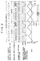
- Fig. 2 shows a channel bit pattern and a DSV obtained after EFM processing with reference to a sampled value by way of example.
- a 16-bit sample is divided into upper eight bits and lower eight bits, which are entered in the modulator via the CIRC encoder to be eight-to-fourteen modulated, providing information bits.
- For the margin bits one of "000”, "001", "010” and "100” is selected. This rule is always-established also at a location linking information bit patterns.
- an EFM signal on a 17-channel-bit basis (or a 27-channel-bit basis in the case of the frame synchronization signal Sf) is output from the modulator at a bit rate of 4.3218 Mbps.
- a period (or recording wavelength) of a low level or a high level of an NRZI recording waveform is always 3T or more and less than 11T as shown in Fig. 2.
- a minimum recording wavelength is 3T and a maximum recording wavelength is 11T.
- T is one period of channel clock 4.3218 MHz.
- this is referred to as an EMF 3T-to-11T rule.
- DSV Digital Sum Variation
- the DSV is given as a time integration of a recording waveform. That is, a variation of the DSV obtained when the high level of the recording waveform continues for a unit time T is +1; the variation obtained when the low level of the recording waveform continues for the unit time T is -1.
- a modulation signal in a period between t 1 and t 2 is not determined straight by 17-channel-bit pattern "01000001000001001"; rather, the modulation signal depends on a level of the signal at time t 1 , that is, a final level of a modulation signal waveform in a period between t 0 and t 1 (this level is hereinafter referred to as a CWLL).
- margin bits to be inserted in a period between t 0+14 and t 1 will be described.
- the DSV obtained when "010" is inserted as the margin bits is indicated with a solid line, while the DSV obtained when "000" is inserted is indicated with a dashed line.
- Fig. 3 shows a prior-art modulator having a margin bit generator.
- An input terminal 10 receives data with one sync frame consisting of 32 symbols from a data generator, not shown. Each 8-bit symbol is eight-to-fourteen modulated by an EFMROM 11 into 14-bit data.
- Frames 0 and 1 of 98 sync frames constituting a subcoding frame are added with 14-bit subcode sync signals S 0 and S 1 as mentioned above.
- the addition of these subcode signals is performed by a subcode sync adder 12 based on a subcode sync timing signal, not shown.
- a 14-bit data Dp including the subcode sync signals S 0 and S 1 and the dummy frame sync signal S'f are sequentially sent to a register 14 to be latched and upper 12 bits are sent to an inhibit margin bit decision circuit 20.
- a last 14-bit data Db hitherto latched in the register 14 are output to a frame sync converter 15 and the inhibit margin bit decision circuit 20 with lower two bits stored in a register 31.
- Lower two bits stored last, or lower two bits of 14-bit data Dbb before the last are supplied from the register 31 to the inhibit margin bit decision circuit 20.
- the inhibit margin bit decision circuit 20 determines margin bits which violate the EFM 3T-to-11T rule and an exceptional inhibit rule. If violating bits are found, the decision circuit sends them to the margin bit generator 40 as an inhibit signal Sinh.
- the inhibit signal Sinh consists of four bits, each of which corresponds to the four types of margin bits "100", “010", "001” and "000". For example, if the first and third margin bits "100" and "001" are inhibited by the EFM 3T-to-11T rule and the exceptional inhibit rule, the 4-bit inhibit signal Sinh is "1010".
- the dummy frame sync adder 13, registers 14, 31 and 32, and inhibit margin bit decision circuit 20 constitute a decision circuit 30.
- the decision circuit 30 receives the 14-bit data Dp coming from the subcode sync adder 12 and the margin bits Mp coming from the margin bit generator 40 and outputs the 14-bit data Db stored last to the frame sync converter 15 and the 4-bit inhibit signal to the margin bit generator 40 indicating that the margin bits Mp should not be used to link the last 14-bit data Db and the current 14-bit data Dp.
- Fig. 4 shows an algorithm for determining inhibit margin bits.
- the inhibit margin bit decision circuit 20 tests bits shown in shadow selected from among the input signals Dp, Db, Mb and Dbb. According to a test result, the decision circuit 20 determines the margin bits Minh not to be used for linking the last 14-bit data Db with the current 14-bit data Dp, sending the 4-bit inhibit signal Sinh to the margin bit generator 40.
- an algorithm for determining the inhibit margin bit Minh by the EFM 3T-to-11T rule is as follows:
- an inhibit margin bit pattern which does not violate the EFM 3T-to-11T rule but is inhibited to prevent erroneous generation of a framing sync signal, or an inhibit margin bit pattern to be inhibited by the exceptional inhibit rule is determined as follows:
- Case 1 the number of "0"s in the end of the last 14-bit data Db is seven and the frame sync signal is generated in a current timing.
- the frame sync converter 15 converts the dummy frame sync signal S'f of sequentially entered 14-bit data into the normal 24-bit frame sync signal Sf based on the frame sync timing, not shown.
- the 14-bit data other than the dummy frame sync signal are supplied to a P/S (Parallel-in/Serial-out) register 16.
- the 24-bit P/S register 16 alternately outputs 14-bit data (or 24-bit data for the frame sync signal Sf) and 3-bit data (margin bits) based on a channel bit clock of 4.3218 MHz.
- a serial signal output from the P/S register at a rate of 4.3218 Mbps is NRZI-modulated by an NRZI circuit 17 to be supplied as an EFM signal to a recording head, not shown, or a laser diode, not shown, via a rotary transformer and a recording amplifier, not shown, for example.
- the EFM signal is then digitally recorded on a CD.
- a DSV integrator 60 Upon receiving the EFM signal, a DSV integrator 60 integrates a DC component of the EFM signal in units of 17 channel bits. Based on a resultant cumulative DSV, the DSV integrator 60 outputs a 3-bit control signal to the margin bit generator 40. For example, if the cumulative DSV is positive in polarity, the bit pattern "001" instructing decrement (-) of the cumulative DSV is output as the control signal. If the cumulative DSV is zero, the bit pattern "010" instructing balance (0) of the cumulative DSV is output. If the cumulative DSV is negative in polarity, the bit pattern "100" instructing increment (+) of the cumulative DSV is output.
- the margin bit generator 40 operates as follows. This circuit outputs a most suitable margin bit pattern of the four types the margin bit patterns "100", “010", "001" and "000".
- the most suitable bit pattern denotes that, when the two pieces of 14-bit data Db and Dp are linked together with this margin bit pattern, the EFM 3T-to-11T rule is also established at the link, no erroneous generation of the frame sync signal occurs, and the cumulative DSV of the EFM signal converges to zero.
- the margin bit generator 40 does not test each margin bit pattern individually for determining the most suitable one; rather, this circuit determines the most suitable pattern from the beginning based on conditions such as the bit patterns of the two pieces of 14-bit data and the cumulative DSV. Input signals to the margin bit generator 40 are as follows.
- a 4-bit inhibit signal Sinh comes from the inhibit margin bit decision circuit 20. If a margin bit pattern violating the EFM 3T-to-11T rule is found or a margin bit pattern which cannot be inserted between the two pieces of 14-bit data Db and Dp because the pattern will erroneously generate the frame sync signal is found, such a pattern is disabled by setting a bit of the inhibit signal corresponding to the margin bit to "1". For example, of the four margin bit patterns "100”, “010", "001" and "000”, if the first and third patterns are disabled, the 4-bit inhibit signal will be "1010".
- a 3-bit control signal is entered in the margin bit generator 40 from the DSV integrator 60 according to the cumulative DSV.
- This 3-bit control signal indicates, from the most significant bit to the least significant bit, that a desired control direction of the cumulative DSV is increment (+), balance (0), and decrement (-). Accordingly, if the cumulative DSV is greater than zero, this control signal is "001" to instruct decrement of the cumulative DSV; if the cumulative DSV is smaller than zero, the control signal is "100" to instruct increment of the cumulative DSV; and if the cumulative DSV is equal to zero, the control signal is "010" to instruct to balance the cumulative DSV as far as possible.
- Fig. 7 shows an example of NRZI waveforms of the two pieces of 14-bit data Db and Dp to be linked together by the margin bits.
- a variation of the cumulative DSV caused by adding the margin bits to the last 14-bit data Db, or a DC component of the margin bits (hereinafter referred to as the DSV of the margin bits) is represented with reference to a low level ("0") of a signal level, or the CWLL of an NRZI waveform at a start of the margin bits.
- a variation of the cumulative DSV caused by linking the 14-bit data Db with following 14-bit data Dp by using 3-bit margin bit pattern, or the 17NWD is obtained by subtracting the 14NWD from the DSV of margin bits for the first, second or third margin bit pattern; for the fourth margin bit pattern ("000"), the variation is obtained by adding the 14NWD to the DSV of margin bits.
- each of (A), (B), (C) and (D) indicates the 17NWD corresponding to each of the four margin bit patters "100", “010", “001” and "000” to be inserted.
- the margin bit pattern "100” is given a second priority
- the margin bit pattern "101” is given a third priority
- the margin bit pattern "001” is given a fourth priority.
- the margin bit patterns "010”, "001", "100” and "000” are prioritized in this order, the most suitable margin bit pattern can be determined straightforwardly.
- the margin bit patterns are prioritized for each of five cases in which the 14NWD of the next 14-bit data Dp is +3 or more, +2, +1, 0 and -1 or less.
- both flags are symmetrical to each other with an x-axis (indicating the 14NWD) in between. Therefore, inverting a sign of an y-axis (indicating the 17NWD) makes the monograph of Fig. 9 be the same as the monograph of Fig. 8.
- reference numeral 41 represents a decoder which decodes the 3-bit control signal with the CWLL signals used as gate signals.
- a truth table of the decoding is shown in Fig. 10 (A).
- Reference numeral 42 represents a decoder for converting the 14NWD represented in a 5-bit two's complement to a 4-bit signal indicating the above-mentioned five cases.
- a truth table of the decoding is shown in Fig. 10 (B).
- Reference numeral 43 represents a programmable logic array (PLA) programmed so that it receives the 4-bit inhibit signal from the inhibit margin bit decision circuit 20, the 3-bit control signal from the decoder 41, and 4-bit signal from the decoder 42 to output a most suitable margin bit pattern 44.
- PLA programmable logic array
- the inhibit signal "X011"
- the most suitable margin bit pattern 44 logically determined by the PLA 43 is output.
- the conventional modulator for example as disclosed in EP-A-0 476 766, controls the margin bit patterns only based on the DSV polarities by a certain gain without monitoring the DSV absolute value. This causes poor convergence when the DSV absolute value is large. When the DSV absolute value is small, an extra gain is added to make the DSV unstable.
- an amplitude of a signal read from a disc on a mini-disc system is as small as about 1/30 of that of a signal read from a full-size compact disc, requiring to control the DSV properly. This requirement has not been fully satisfied due to the above-mentioned problem.
- EP-A-0 535 560 which was published after the priority and filing dates of the present application (Article 54(3) EPC), discloses a modulator in which DSV variation of a channel bit pattern signal is provided with a saturation characteristic so as to prevent output divergence.
- a margin bit generating circuit receives a number of signals for selecting the margin bit pattern.
- JP-A-62 281 523 discloses a modulator having convergence characteristics set by a margin bit selection circuit receiving signals indicative of DSV, polarity, a DSV after a margin bit and a rule violation signal.
- a modulator wherein input m bit code series are converted to n channel bit patterns (where n > m) which are linked to each other with one of a plurality of margin bit patterns to limit maximum and minimum recording wavelengths and suppress a low-frequency component of a recording waveform, said modulator comprising margin bit generating means for selecting a margin bit pattern most suitable for controlling a cumulative digital sum variation from among said plurality of margin bit patterns on the basis of the following signals supplied to said margin bit generating means:
- a preferred embodiment of the present invention is capable of monitoring the DSV absolute value to generate a margin bit pattern having a proper gain, thereby improving the convergence of the DSV.
- Fig. 13 which illustrates a preferred embodiment of the invention, the following four types of signals are entered in a margin bit generator 40A.
- the bits in the 4-bit inhibit signal correspond, from a most significant bit to a least significant bit, to the margin bit patterns "001", “010", “100” and "000” for example.
- Flag "1" is set to any of the margin bit patterns that violates the EFM 3T-to-11T rule and/or erroneously generates a frame sync.
- the margin bit pattern "000” is inhibited by the EFM 3T-to-11T rule and the 4-bit inhibit signal "0001" is sent from the inhibit margin bit decision circuit 20 to a programmable logic array (PLA) 43A shown in Fig. 17.
- PPA programmable logic array
- the above-mentioned 3-bit control signal coming from the DSV integrator 60A is sent to the PLA 43A via a decoder 41A which uses the CWLL signal as a gate signal.
- the decoder 41A based on CWLL and DSV polarities, converts the 3-bit control signal and sends a resultant signal to the PLA 43A so that the PLA 43A outputs the most suitable margin bit pattern 44A.
- the DSV of the 14-bit data Dp, or a variation (14NWD) of cumulative DSV resulted from adding the 14-bit data Dp to the end of a margin bit pattern is represented in a 5-bit two's complement and is entered as a 14NWD signal in a decoder 42A to be decoded into one of four cases that follow:
- the PLA 43A outputs the most suitable margin bit pattern 44A based on combinations of the input signals consisting of a total of 10 bits (the 4-bit signal indicating an inhibit margin bit pattern, the 3-bit control signal instructing control direction of the cumulative DSV and its gain, and 3-bit signal indicating one of the four cases of 14NWD).
- Fig. 13 The basic constitution of the modulator practiced as a preferred embodiment of the invention as shown in Fig. 13 is generally similar to that of Fig. 3, and therefore description of overlapping portions will be omitted.
- a DSV integrator 60A operates differently from the previously-proposed DSV integrator 60 of Fig. 3. Further, unlike the previously-proposed circuit, the preferred embodiment includes a decision circuit 70 for determining a zero-cross point of a DSV integrated value and a margin bit replacing circuit 80.
- a serial signal having been NRZI-converted by an NRZI circuit 17, is output from the modulator at a rate of 4.3218 Mbps as an EFM signal to a recording head or a laser diode, both not shown, via a rotary transformer and a recording amplifier, both not shown, for example, to be eventually recorded on a compact disc (CD) in a digital manner.
- CD compact disc
- the DSV integrator 60A integrates a DC component of the signal in units of 17 channel bits.
- the cumulative DSV cannot be directed as desired due to reasons such as presence of an inhibit margin bit pattern. If the cumulative DSV is positive, its absolute value gets larger and larger because a margin bit pattern to put the cumulative DSV in a negative direction cannot be selected, eventually causing the DSV integrator to overflow (actually, a decoder or an overflow limiter 63 of Fig. 18 operates).
- a margin bit replacing circuit 80 is provided for this purpose.
- Fig. 13 suppose that data 93 having a pattern "10010011" enters in a terminal 10. The data is converted by an EFMROM 11 into a 14-bit pattern "00100000100001". If this pattern comes one after another continuously, a margin bit pattern "001" or "000” of Fig. 12 is selected for an inhibit margin bit pattern by the EFM 3T-to-11T rule.
- the margin bit replacing circuit 80 measures how long it has passed since a last zero-crossing of the cumulative DSV.
- a more than certain time is forcibly replaced with another in the range permitted by the EFM 3T-to-11T rule.
- the most suitable margin bit pattern is not only simply replaced; additonally, such a margin bit pattern containing "1" as “100", “010” or “001” is converted to "000” and the margin bit pattern "000” is converted to "100", "010” or "001” within the range permitted by the inhibit margin bit pattern.
- the 17NWD becomes -3; however the CWLL goes high starting with a next symbol to make the 17NWD go up to +1, forcibly putting the cumulative DSV in a zero-converging direction.
- a margin bit generator 40A operates as follows.
- the margin bit generator 40A outputs a most suitable margin bit pattern from among the four types of the margin bit patterns "100", “010", “001” and "000” mentioned above.
- the margin bit generator 40A monitors a magnitude of the absolute value of the cumulative DSV to output a margin bit pattern having a proper gain. Signals to enter this circuit are as follows.
- a 4-bit inhibit signal comes from the inhibit margin bit decision circuit 20.
- This 4-bit inhibit signal indicates that a margin bit pattern cannot be inserted between two pieces of 14-bit data Db and Dp because the pattern violates the EFM 3T-to-11T rule or erroneously generates a frame sync signal.
- the indication is made by setting a bit corresponding to the margin bit pattern to "1". For example, of the four types of margin bit patterns "100”, “010", "001" and "000”, if the first and third patterns are inhibited, this 4-bit inhibit signal becomes "1010".
- a 3-bit control signal comes from the DSV integrator 60A according to the cumulative DSV.
- a most significant bit of this 3-bit control signal indicates a desirable control direction of the cumulative DSV is an increment direction (+).
- a mid bit of the control signal instructs a maximum gain or a minimum gain to be used for directing the cumulative DSV.
- a least significant bit of the control signal indicates that the desirable control direction of the cumulative DSV is an decrement direction (-).
- a monograph for obtaining a 17NWD from a 14NWD is the same as used in the prior-art technology.
- Fig. 18 shows a preferred embodiment of the DSV integrator 60A.
- a DSV integrator 65 increments by one (+1) when a EFM signal is high for one T based on a channel clock (4.3218 MHz) and decrements by one (-1) when the EFM signal is low for one T. Since this integrator 65 consists of eight bits and a signal to handle is represented in a two's complement, up to ⁇ 128 states are represented.
- a most significant bit of the integrator 65 indicates a sign of an integrated value: when this bit is "0", it indicates a plus sign; when this bit is "1", it indicates a minus sign.
- This sign decision is performed by a decoder 62 of Fig. 18.
- the most significant bit of the integrator 65 provides a DSVM signal, or the sign bit. When this bit is "1", the cumulative DSV is negative.
- An 8-input NOR circuit 62a in the decoder 62 detects that the integrated value is ⁇ 0. An output of the NOR circuit is NORed with the DSVM to output DSVP. That is, if the cumulative DSV is neither negative nor 0, it is positive.
- a decoder 61 determines a magnitude of an absolute value of the cumulative DSV. If upper six bits of the 8-bit integrator 65 are all “0"s or all “1”s (-4 ⁇ DSV ⁇ +3), the ABSM is set to "0" to send a minimum gain instruction to a margin bit generating PLA 40A.
- the decoder 63 is an overflow limiter of the integrator 65 and issues an increment inhibit instruction when the cumulative DSV is +127 and a decrement inhibit instruction when the cumulative DSV is -128. Controlling an enable EN of the DSV integrator 65 by these instructions prevents the DSV integrator from overflowing.
- Fig. 20 shows a truth table for the decoder 41A.
- a decoder 42A converts the 14NWD represented in a 5-bit two's complement into a 4-bit signal that represents the above-mentioned five cases.
- Fig. 21 shows a truth table for the decoder 42A.
- Reference numeral 43A indicates a PLA programmed beforehand so that it outputs the most suitable margin bit pattern 44A from the 4-bit inhibit signal supplied from the inhibit margin bit decision circuit 20, the 3-bit control signal supplied from the decoder 41A, and the 5-bit signal supplied from the decoder 42A.
- Fig. 22 shows a truth table preprogrammed in the PLA 43A.
- the inhibit signal "X011"
- the most suitable margin bit pattern 44A logically determined by the PLA 43A is output.
- the DSV converges to zero.
- the margin bit pattern "001" or "000” there are the two types of margin bit patterns that cause the DSV to converge to zero. Since the DSV has a large absolute value, it is ideally desirable that the 17NWD be negative and large in value. Hence, the margin bit pattern "001" is selected under such a condition.
- margin bit patterns that make the 17NWD negative. Since the DSV is positive and large in value, it is advantageous for the 17NWD to be negative and large in value in converging the DSV. Hence, in the above-mentioned conditions, the margin bit pattern "001" is selected.
- the conventional technique selects the margin bit pattern "010", so that the DSV changes in its magnitude as small as from +29 to +26.
- Fig. 24 shows curves obtained by plotting the above-mentioned DSV transitions.
- Curve 95 is obtained by the conventional control technique, while curve 96 is obtained by the novel art.
- a difference in speed in converging the DSV which has greatly deviated from zero because of the inhibit margin bit pattern or the like is obvious between both the techniques. It should be noted that the curves of Fig. 24 have been obtained by supposing that the CWLL of all data is low and there are no margin bit pattern.
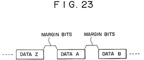
- the margin bit patterns that take the DSV in a converging direction are "100" and "010". Of these margin bit patterns, "100" is more excellent in zero-convergence because the DSV up to data "Z" is -4 as long as this one symbol is concerned.
- margin bit pattern "100” is selected here, there is no inhibit margin bit pattern because the 14NWD of next data "B" is also supposed to be ⁇ 0. And if the CWLL is also low, "100" is also selected as a margin bit pattern to be added to the data "B". This is the selection represented by the DSV curve of Fig. 25 obtained by the conventional control technique. Although the zero convergence is excellent in this case, the DSV zero-crossing is heavy, making the curve unstable.
- the DSV is drawn back as small as from -4 to -3 for a single symbol. However, if the same condition continues, the DSV curve finely converges to zero from -4 to -3 to -2 to -1 to ⁇ 0.
- the DSV obtained according to the present invention has no excess zero-cross and its value is more stable than that obtained by the prior-art technique as shown in Fig. 25.
- control for drawing the DSV back to zero is made by monitoring the absolute value of the DSV (by controlling the maximum and minimum gains), resulting in following advantages:
- margin bit patterns that satisfy the EFM 3T-to-11T rule are first selected at a connection between information bit patterns; then a margin bit pattern most suitable for bringing the DSV to zero by monitoring the absolute value of the DSV and with a suitable gain is selected from the first selected group.
- the above-mentioned technological concept according to this invention applies in general to any modulating circuit that converts an input m bit codes to n channel bit patterns (where n >m) which are linked to each other with one of multiple margin bit patterns to limit maximum and minimum recording wavelengths and suppress a low frequency component of a recording waveform.
- the above-mentioned modulator having the margin bit generator embodying the invention allows the convergence of the cumulative DSV to be enhanced and instability caused by convergence control to be eliminated by monitoring the absolute value of the cumulative DSV and using a proper gain, unlike the previously-proposed method in which the margin bit pattern most suitable for the convergence control is selected based only on the polarity of the cumulative DSV.
Landscapes
- Engineering & Computer Science (AREA)
- Signal Processing (AREA)
- Theoretical Computer Science (AREA)
- Signal Processing For Digital Recording And Reproducing (AREA)
Claims (9)
- Modulator, bei dem eingegebene Codeserien mit m Bit in n Kanal-Bitmuster (wobei n > m) umgesetzt werden, die miteinander durch eines von mehreren Randbitmustern verbunden werden, um die minimale und maximale Aufzeichnungs-Wellenlänge zu begrenzen und eine niederfrequente Komponente eines Aufzeichnungs-Signalverlaufs zu unterdrücken, wobei der Modulator eine Randbit-Erzeugungseinrichtung (40A) zur Auswahl eines zur Steuerung einer kumulativen digitalen Summenvariation (DSV) geeignetsten Randbitmusters aus den mehreren Randbitmustern auf Grundlage der folgenden, der Randbit-Erzeugungseinrichtung (40A) zugeführten Signale aufweist:ein Signal (Sinh) hinsichtlich eines der mehreren Randbitmuster, das gesperrt werden soll,ein Signal (CWLL) hinsichtlich des abschließenden Signalverlaufspegels von jedem der n Kanal-Bitmuster, das vor jedem der mehreren Randbitmuster angeordnet werden soll,ein Steuersignal (DSVP, DSVM) hinsichtlich der Polarität der kumulativen digitalen Summenvariation (DSV), undein Signal hinsichtlich der kumulativen digitalen Summenvariation (DSV) von jedem der n Kanal-Bitmuster, die nach jedem der mehreren Randbitmustern angeordnet werden sollen,dadurch gekennzeichnet, daß weiterhin die folgenden Signale zu der Randbit-Erzeugungseinrichtung (40A) zur Wahl des Randbitmusters gegeben werden:ein Steuersignal (ABSM) hinsichtlich des Betrags des Absolutwerts der digitalen Summenvariation (DSV), undein Steuersignal zur Einstellung des Faktors der digitalen Summenvariation (DSV) als Antwort auf den Betrag des Amplitudenwerts der digitalen Summenvariation (DSV).
- Modulator nach Anspruch 1,
bei dem das Steuersignal hinsichtlich der Polarität einer kumulativen digitalen Summenvariation (DSV) aus einem Signal (DSVP), das anzeigt, daß die Polarität der digitalen Summenvariation (DSV) positiv ist, und einem Signal (DSVM) besteht, das anzeigt, daß die Polarität der digitalen Summenvariation (DSV) negativ ist, und das Signal (ABSM) hinsichtlich des Betrags des Absolutwerts der kumulativen digitalen Summenvariation (DSV) anzeigt, daß die kumulative digitale Summenvariation (DSV) durch einen maximalen Faktor oder einen minimalen Faktor entsprechend des Betrags des Absolutwerts der kumulativen digitalen Summenvariation (DSV) auf Null gezogen werden soll. - Modulator nach Anspruch 1 oder 2, aufweisend:eine Entscheidungsschaltung (70) zur Bestimmung eines Auftretens eines Nulldurchgangs der kumulativen digitalen Summenvariation (DSV), undeine Ersetzungseinrichtung (80) zur Messung der Zeit, die nach dem Auftreten des Nulldurchgangs der kumulativen digitalen Summenvariation (DSV) verstrichen ist, um zwangsweise nach dem Verstreichen einer gewissen Zeit nach dem Auftreten des Nulldurchgangs ein von der Randbit-Erzeugungseinrichtung (40A) ausgegebenes Randbitmuster durch ein anderes zu ersetzen.
- Modulator nach einem der Ansprüche 1 bis 3,
bei dem das Steuersignal zur Einstellung des Faktors der digitalen Summenvariation (DSV) den Faktor bei einem vorbestimmten Wert des Absolutwerts der digitalen Summenvariation (DSV) verringert. - Modulator nach Anspruch 4,
bei dem der vorbestimmte Wert des Absolutwerts der digitalen Summenvariation (DSV) kleiner oder gleich 4 ist. - Modulator nach einem der vorhergehenden Ansprüche,
der auf ein Steuersignal zur Begrenzung eines Überlaufsignals der digitalen Summenvariation (DSV) antwortet. - Modulator nach Anspruch 6,
bei dem das Überlaufsignal auf eine vorbestimmte Zeit nach dem Nulldurchgang der kumulativen digitalen Summenvariation (DSV) begrenzt ist. - Modulator nach Anspruch 7,
bei dem die vorbestimmte Zeitdauer gleich 32 Symbole beträgt. - Modulator nach Anspruch 7,
bei dem die vorbestimmte Zeitdauer ungefähr 136 µs beträgt.
Applications Claiming Priority (2)
| Application Number | Priority Date | Filing Date | Title |
|---|---|---|---|
| JP28431992A JP3355666B2 (ja) | 1992-10-22 | 1992-10-22 | 変調回路 |
| JP284319/92 | 1992-10-22 |
Publications (2)
| Publication Number | Publication Date |
|---|---|
| EP0594413A1 EP0594413A1 (de) | 1994-04-27 |
| EP0594413B1 true EP0594413B1 (de) | 1997-09-03 |
Family
ID=17677015
Family Applications (1)
| Application Number | Title | Priority Date | Filing Date |
|---|---|---|---|
| EP93308352A Expired - Lifetime EP0594413B1 (de) | 1992-10-22 | 1993-10-20 | Modulator mit Kontrolle einer laufenden Digitalsumme |
Country Status (5)
| Country | Link |
|---|---|
| US (1) | US5486827A (de) |
| EP (1) | EP0594413B1 (de) |
| JP (1) | JP3355666B2 (de) |
| KR (1) | KR100263691B1 (de) |
| DE (1) | DE69313581T2 (de) |
Families Citing this family (9)
| Publication number | Priority date | Publication date | Assignee | Title |
|---|---|---|---|---|
| JP3464558B2 (ja) * | 1995-03-31 | 2003-11-10 | 富士通株式会社 | エンコード装置及び記憶装置 |
| US5574448A (en) * | 1995-05-08 | 1996-11-12 | Quantum Corporation | Method and apparatus for encoding data with variable block lengths |
| JP3661890B2 (ja) * | 1995-12-15 | 2005-06-22 | ソニー株式会社 | 画像データ送信方法及び画像データ受信方法 |
| DE69706871T2 (de) * | 1997-10-21 | 2002-04-11 | Hewlett-Packard Co. (N.D.Ges.D.Staates Delaware), Palo Alto | Verfahren zur Verhinderung des Kopierens von digitalen Daten |
| JP4717208B2 (ja) | 1998-02-27 | 2011-07-06 | ダグ カーソン アンド アソシエーツ,インク. | 光ディスクマスタ作成プロセスにおけるピットおよびランド遷移ロケーションの個別調整方法、およびそのための最適化回路 |
| JP2003323761A (ja) * | 2002-05-02 | 2003-11-14 | Sony Corp | デジタルデータの記録媒体、記録方法、記録装置、再生方法、再生装置、送信方法および送信装置 |
| TW594700B (en) * | 2002-06-07 | 2004-06-21 | Mediatek Inc | Method for performing DSV protection on EFM/EFM+ encoding system and its device |
| CN100392740C (zh) * | 2002-09-24 | 2008-06-04 | 联发科技股份有限公司 | 一种对编码系统做数字总和值保护的方法及装置 |
| DK2573166T3 (da) * | 2004-02-26 | 2016-07-04 | Immunovative Therapies Ltd | Fremgangsmåder til fremstilling af T-celler til celleterapi |
Family Cites Families (9)
| Publication number | Priority date | Publication date | Assignee | Title |
|---|---|---|---|---|
| EP0178813B1 (de) * | 1984-10-01 | 1993-08-18 | Matsushita Electric Industrial Co., Ltd. | Verfahren und Vorrichtung zur numerischen Datenkodierung |
| JP2656024B2 (ja) * | 1986-05-29 | 1997-09-24 | 松下電器産業株式会社 | 変調回路 |
| NL8801076A (nl) * | 1988-04-26 | 1989-11-16 | Philips Nv | Inrichting voor het optekenen van een digitaal informatiesignaal. |
| JP2974678B2 (ja) * | 1988-06-23 | 1999-11-10 | ソニー株式会社 | データ誤り検出方式 |
| JP2809832B2 (ja) * | 1990-07-13 | 1998-10-15 | 株式会社東芝 | 符号変調方法 |
| NL9002070A (nl) * | 1990-09-21 | 1992-04-16 | Philips Nv | Inrichting voor het optekenen van een digitaal informatiesignaal in een registratiedrager. |
| JP2741112B2 (ja) * | 1991-03-29 | 1998-04-15 | シャープ株式会社 | ディジタル変調方式およびディジタル変調装置 |
| EP0511498B1 (de) * | 1991-03-30 | 1998-12-09 | Kabushiki Kaisha Toshiba | Kodiereinrichtung für digitale Signale mit verbesserter Kanal-Blockkodierung |
| US5349349A (en) * | 1991-09-30 | 1994-09-20 | Sony Corporation | Modulator circuit for a recording for a digital recording medium |
-
1992
- 1992-10-22 JP JP28431992A patent/JP3355666B2/ja not_active Expired - Lifetime
-
1993
- 1993-10-18 US US08/136,949 patent/US5486827A/en not_active Expired - Lifetime
- 1993-10-20 DE DE69313581T patent/DE69313581T2/de not_active Expired - Fee Related
- 1993-10-20 EP EP93308352A patent/EP0594413B1/de not_active Expired - Lifetime
- 1993-10-22 KR KR1019930022004A patent/KR100263691B1/ko not_active IP Right Cessation
Also Published As
| Publication number | Publication date |
|---|---|
| US5486827A (en) | 1996-01-23 |
| DE69313581T2 (de) | 1998-03-26 |
| JP3355666B2 (ja) | 2002-12-09 |
| DE69313581D1 (de) | 1997-10-09 |
| KR940010046A (ko) | 1994-05-24 |
| KR100263691B1 (ko) | 2000-08-01 |
| JPH06139708A (ja) | 1994-05-20 |
| EP0594413A1 (de) | 1994-04-27 |
Similar Documents
| Publication | Publication Date | Title |
|---|---|---|
| US4760378A (en) | Method and apparatus for converting a run length limited code | |
| US4677421A (en) | Digital information signal encoding method with reduced run length and improved self-clocking | |
| KR0165441B1 (ko) | 디지털 데이터 채널 부호화 및 복호화방법과 그 장치 | |
| EP1168331B1 (de) | Signaldemodulationsverfahren und Signaldemodulationsvorrichtung | |
| US4833471A (en) | Data processing apparatus | |
| JPH05266600A (ja) | 2値符号記録媒体 | |
| EP0625828A2 (de) | Modulationsverfahren und -vorrichtung und Demodulationsvorrichtung | |
| EP0535560A2 (de) | Modulatorschaltung für die Regenerierung eines digitalen Aufzeichnungsmediums | |
| EP0594413B1 (de) | Modulator mit Kontrolle einer laufenden Digitalsumme | |
| US7519119B2 (en) | Method and apparatus of converting a series of data words into a modulated signal | |
| US5508701A (en) | Data conversion method and recording and reproduction apparatus | |
| EP0557130A2 (de) | Datenumsetzungsverfahren und Aufzeichnungs-/Wiedergabegerät zur Durchführung desselben | |
| JP2805096B2 (ja) | ディジタル変調方法及び復調方法 | |
| US6778105B2 (en) | Method of modulating series of data words into constrained sequence | |
| US6731228B2 (en) | Method and apparatus of converting a series of data words into a modulated signal | |
| KR0144965B1 (ko) | 이.에프.엠.(efm)복조의 에러정정방법 | |
| EP1425858A2 (de) | Kodierungsverfahren und vorrichtung | |
| KR100817936B1 (ko) | 일련의 데이터 워드를 변조신호로 변환하는 방법 및 장치 | |
| JPH01175323A (ja) | 8/9符号変換方式 | |
| JPH0683272B2 (ja) | 8−12変調方法 | |
| JPH0746481B2 (ja) | デイジタル変調装置 | |
| JPH06111487A (ja) | 変調回路 |
Legal Events
| Date | Code | Title | Description |
|---|---|---|---|
| PUAI | Public reference made under article 153(3) epc to a published international application that has entered the european phase |
Free format text: ORIGINAL CODE: 0009012 |
|
| AK | Designated contracting states |
Kind code of ref document: A1 Designated state(s): DE FR GB |
|
| 17P | Request for examination filed |
Effective date: 19940929 |
|
| 17Q | First examination report despatched |
Effective date: 19960524 |
|
| GRAG | Despatch of communication of intention to grant |
Free format text: ORIGINAL CODE: EPIDOS AGRA |
|
| GRAH | Despatch of communication of intention to grant a patent |
Free format text: ORIGINAL CODE: EPIDOS IGRA |
|
| GRAH | Despatch of communication of intention to grant a patent |
Free format text: ORIGINAL CODE: EPIDOS IGRA |
|
| GRAA | (expected) grant |
Free format text: ORIGINAL CODE: 0009210 |
|
| AK | Designated contracting states |
Kind code of ref document: B1 Designated state(s): DE FR GB |
|
| REF | Corresponds to: |
Ref document number: 69313581 Country of ref document: DE Date of ref document: 19971009 |
|
| ET | Fr: translation filed | ||
| PLBE | No opposition filed within time limit |
Free format text: ORIGINAL CODE: 0009261 |
|
| STAA | Information on the status of an ep patent application or granted ep patent |
Free format text: STATUS: NO OPPOSITION FILED WITHIN TIME LIMIT |
|
| 26N | No opposition filed | ||
| REG | Reference to a national code |
Ref country code: GB Ref legal event code: IF02 |
|
| PGFP | Annual fee paid to national office [announced via postgrant information from national office to epo] |
Ref country code: FR Payment date: 20031003 Year of fee payment: 11 |
|
| PGFP | Annual fee paid to national office [announced via postgrant information from national office to epo] |
Ref country code: GB Payment date: 20031016 Year of fee payment: 11 |
|
| PGFP | Annual fee paid to national office [announced via postgrant information from national office to epo] |
Ref country code: DE Payment date: 20031030 Year of fee payment: 11 |
|
| PG25 | Lapsed in a contracting state [announced via postgrant information from national office to epo] |
Ref country code: GB Free format text: LAPSE BECAUSE OF NON-PAYMENT OF DUE FEES Effective date: 20041020 |
|
| PG25 | Lapsed in a contracting state [announced via postgrant information from national office to epo] |
Ref country code: DE Free format text: LAPSE BECAUSE OF NON-PAYMENT OF DUE FEES Effective date: 20050503 |
|
| GBPC | Gb: european patent ceased through non-payment of renewal fee |
Effective date: 20041020 |
|
| PG25 | Lapsed in a contracting state [announced via postgrant information from national office to epo] |
Ref country code: FR Free format text: LAPSE BECAUSE OF NON-PAYMENT OF DUE FEES Effective date: 20050630 |
|
| REG | Reference to a national code |
Ref country code: FR Ref legal event code: ST |