EP0592671A1 - Halbleiterkörper und verfahren zu dessen reinigung - Google Patents
Halbleiterkörper und verfahren zu dessen reinigung Download PDFInfo
- Publication number
- EP0592671A1 EP0592671A1 EP92914382A EP92914382A EP0592671A1 EP 0592671 A1 EP0592671 A1 EP 0592671A1 EP 92914382 A EP92914382 A EP 92914382A EP 92914382 A EP92914382 A EP 92914382A EP 0592671 A1 EP0592671 A1 EP 0592671A1
- Authority
- EP
- European Patent Office
- Prior art keywords
- silicon wafer
- wafer
- oxide film
- nh4oh
- washing
- Prior art date
- Legal status (The legal status is an assumption and is not a legal conclusion. Google has not performed a legal analysis and makes no representation as to the accuracy of the status listed.)
- Withdrawn
Links
Images
Classifications
-
- H—ELECTRICITY
- H01—ELECTRIC ELEMENTS
- H01L—SEMICONDUCTOR DEVICES NOT COVERED BY CLASS H10
- H01L21/00—Processes or apparatus adapted for the manufacture or treatment of semiconductor or solid state devices or of parts thereof
- H01L21/02—Manufacture or treatment of semiconductor devices or of parts thereof
- H01L21/02041—Cleaning
- H01L21/02043—Cleaning before device manufacture, i.e. Begin-Of-Line process
- H01L21/02052—Wet cleaning only
Definitions
- the present invention relates to a silicon wafer for use in LSI manufacturing, and in particular, relates to a silicon wafer having little empty lattice on the wafer surface thereof.
- the present inventors have discovered the following with respect to the relationship among the washing method, the state of the wafer surface after washing, and the element characteristics, as a result of intensive research with respect to washing methods of silicon wafers.
- a silicon monocrystal produced by the pull method was sliced, and the surface roughnesses Ra of the CZ silicon wafers which were obtained by mirror polishing the slices were measured by means of a scanning tunnelling microscope, and were found to be within approximately a range of 0.1 -0.4 nanometers.
- surface roughness Ra represents the average central surface roughness, and represents an averaging of the absolute values of the size of the imperfections from the center line along which imperfections were averaged.
- the roughening of the surface of the silicon wafer as a result of NH4OH-H2O2 washing is thought by the present inventors to take place as a result of the interpolation of the empty lattice of the silicon. That is to say, in the first washing, the silicon surface is subjected to etching on a level of approximately 80 angstroms; however, when an empty lattice exists, isotropic etching cannot be conducted, and anisotropic acid etching occurs as a result of the empty lattice, so that the periphery of the empty lattice is etched to a greater degree, and it is thought that as a result, the surface becomes rough.
- the present invention has as an object thereof to provide a silicon wafer which is capable of suppressing the surface roughness of the wafer resulting from NH4OH-H2O2 washing with respect to large diameter wafers having a diameter of 8 inches or more, and which is capable of forming high performance elements.
- a first feature of the present invention resides in a silicon wafer, characterized in that a thermal oxide film is formed over the entirety of the surface of a silicon wafer having a diameter of 8 inches or more which is obtained by the slicing of an ingot produced by means of the pull method.
- a second feature of the present invention resides in a wafer cleaning method, characterized in that after a thermal oxide film is removed from the silicon wafer of the first feature, the entire surface of the wafer is washed with NH4OH-H2O2.
- the silicon wafers of the present invention are sliced from an ingot produced by means of the pull method, are subjected to mirror polishing, and are washed, and then these are heated and oxidized in an oxidizing atmosphere of, for example, an oxidation furnace or the like, and a thermal oxide film is thus formed on the surface thereof.
- thermal oxidizing treatment By combining temperature, oxidizing gas or moisture concentration, flow rate, time period, and the like, various conditions can be selected for the thermal oxidizing treatment; however, conditions which produce an oxide film thickness of 0.7 micrometers are desirable.
- a 0.7 micrometer thermal oxide film may be produced, for example, by means of wet oxidizing at a temperature of 1000°C and for a period of 4 hours.
- dry oxidizing may also be employed.
- the thickness of the surface layer in which the above empty lattice density is reduced be 800 angstroms or greater.
- the roughening of the surface will be suppressed, and when elements are produced on a wafer which has been subjected to this type of treatment, the element characteristics, such as, for example, the dielectric breakdown voltage, the MOS characteristics, and the like, will be greatly improved.
- the oxide film may be removed from the silicon wafer after the formation thereof by means of etching; however, if thermal oxide film remains on the silicon wafer, it is possible to prevent the occurrence of damage to the wafer resulting from collision with cases and the like during silicon wafer transportation, and to prevent the adhesion of particles, such as debris and the like, to the silicon surface.
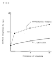
- Figure 1 is a graph showing the relationship between NH4OH-H2O2 washing and silicon wafer surface roughness Ra.
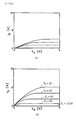
- Figure 2 shows graphs indicating the current (I D ) - voltage (V D ) characteristics of an n-channel MOS; (a) indicates a conventional example, while (b) indicates that of the embodiment.
- a CZ silicon wafer having a diameter of 8 inches was placed in an oxidizing furnace at a temperature of 1000°C, and was heated for a period of 4 hours under a gas flow of 1 L/min of H2 and 1 L/min of O2, and a thermal oxide film of 0.7 micrometers was formed on the wafer surface.
- the thermal oxide film was subjected to etching using a hydrofluoric acid buffer solution (NH4OH + HF + H2O), and was washed for a period of 10 minutes in an NH4OH-H2O2-H2O (1:1:5) washing solution.
- the surface roughness Ra after washing was measured with a scanning tunneling microscope and the results thereof are shown in Figure 1.
- the surface roughness Ra of a conventional wafer which was not subjected to thermal oxide film formation but which was subjected to NH4OH-H2O2 washing, was measured in the same manner. The results thereof are also shown in Figure 1.
- the conventional wafer which was not subjected to thermal oxide film formation, had a surface roughness of 0.15 micrometers prior to washing, and the surface roughness increased to 0.45 micrometers after 10 minutes of washing, and when washing was repeated 10 times, the surface roughness increased to 0.65 micrometers.
- the wafer of the present embodiment had a surface roughness of 0.2 nanometers after one washing, thus representing almost no change in surface roughness, and even after 10 washings, the surface roughness was 0.35 micrometers, so that the approximate surface state after wafer polishing was maintained.
- the thickness of the surface layer in which the empty lattice density is reduced is 800 angstroms or more, so that no adverse effects will be exerted on the devices formed on the wafer surface. Furthermore, it became clear that the density was reduced to 1/10th that of bulk density or less. This was confirmed by results of measurements of the wafers of the present embodiment and the conventional wafers using the DLTS method (Deep Level Transient Spectroscopy).
- the thermal oxide film which is produced on the silicon wafer of the present embodiment exhibits extremely desirable characteristics as an insulating film in comparison with the conventional silicon wafer.
- the present invention it is possible to suppress the roughening of the surface caused by washing with NH4OH-H2O2, so that it becomes possible to provide a silicon wafer for use in high-performance elements having, for example, a thin gate oxide film or capacitor. Furthermore, it has become possible to prevent damage to the silicon wafer resulting from collision with cases and the like during transport, and to prevent the adhesion of particles such as debris or the like to the silicon.
Landscapes
- Engineering & Computer Science (AREA)
- Physics & Mathematics (AREA)
- Condensed Matter Physics & Semiconductors (AREA)
- General Physics & Mathematics (AREA)
- Manufacturing & Machinery (AREA)
- Computer Hardware Design (AREA)
- Microelectronics & Electronic Packaging (AREA)
- Power Engineering (AREA)
- Formation Of Insulating Films (AREA)
- Cleaning Or Drying Semiconductors (AREA)
Applications Claiming Priority (3)
| Application Number | Priority Date | Filing Date | Title |
|---|---|---|---|
| JP18814891A JPH0513395A (ja) | 1991-07-02 | 1991-07-02 | シリコンウエハ−及び洗浄方法 |
| JP188148/91 | 1991-07-02 | ||
| PCT/JP1992/000839 WO1993001615A1 (en) | 1991-07-02 | 1992-07-02 | Silicon wafer and its cleaning method |
Publications (1)
| Publication Number | Publication Date |
|---|---|
| EP0592671A1 true EP0592671A1 (de) | 1994-04-20 |
Family
ID=16218592
Family Applications (1)
| Application Number | Title | Priority Date | Filing Date |
|---|---|---|---|
| EP92914382A Withdrawn EP0592671A1 (de) | 1991-07-02 | 1992-07-02 | Halbleiterkörper und verfahren zu dessen reinigung |
Country Status (3)
| Country | Link |
|---|---|
| EP (1) | EP0592671A1 (de) |
| JP (1) | JPH0513395A (de) |
| WO (1) | WO1993001615A1 (de) |
Cited By (2)
| Publication number | Priority date | Publication date | Assignee | Title |
|---|---|---|---|---|
| WO2001053582A1 (en) | 2000-01-19 | 2001-07-26 | Benetton Group S.P.A. | Vibration absorbing device, particularly for shoes or sports implements |
| US8043871B2 (en) | 2008-04-25 | 2011-10-25 | Shin-Etsu Handotai Co., Ltd. | Method for forming oxide film on silicon wafer |
Families Citing this family (3)
| Publication number | Priority date | Publication date | Assignee | Title |
|---|---|---|---|---|
| US6348157B1 (en) | 1997-06-13 | 2002-02-19 | Tadahiro Ohmi | Cleaning method |
| JP4135780B2 (ja) * | 1997-08-29 | 2008-08-20 | ユーシーティー株式会社 | 薬液定量注入装置および方法 |
| CN111842330A (zh) * | 2020-07-31 | 2020-10-30 | 江苏高照新能源发展有限公司 | 一种单晶硅片清洗装置及工艺 |
Family Cites Families (3)
| Publication number | Priority date | Publication date | Assignee | Title |
|---|---|---|---|---|
| JPS58168237A (ja) * | 1982-03-30 | 1983-10-04 | Toshiba Corp | シリコン基板 |
| JPS60247928A (ja) * | 1984-05-23 | 1985-12-07 | Seiko Instr & Electronics Ltd | 半導体基板の洗浄方法 |
| JPS61294824A (ja) * | 1985-06-21 | 1986-12-25 | Nec Corp | 半導体集積回路の製造装置 |
-
1991
- 1991-07-02 JP JP18814891A patent/JPH0513395A/ja active Pending
-
1992
- 1992-07-02 WO PCT/JP1992/000839 patent/WO1993001615A1/ja not_active Application Discontinuation
- 1992-07-02 EP EP92914382A patent/EP0592671A1/de not_active Withdrawn
Non-Patent Citations (1)
| Title |
|---|
| See references of WO9301615A1 * |
Cited By (2)
| Publication number | Priority date | Publication date | Assignee | Title |
|---|---|---|---|---|
| WO2001053582A1 (en) | 2000-01-19 | 2001-07-26 | Benetton Group S.P.A. | Vibration absorbing device, particularly for shoes or sports implements |
| US8043871B2 (en) | 2008-04-25 | 2011-10-25 | Shin-Etsu Handotai Co., Ltd. | Method for forming oxide film on silicon wafer |
Also Published As
| Publication number | Publication date |
|---|---|
| JPH0513395A (ja) | 1993-01-22 |
| WO1993001615A1 (en) | 1993-01-21 |
Similar Documents
| Publication | Publication Date | Title |
|---|---|---|
| JP4486753B2 (ja) | 単結晶シリコン基板上に単結晶ゲルマニウム層を得る方法およびそれにより得られた生成物 | |
| US6376335B1 (en) | Semiconductor wafer manufacturing process | |
| JPH0793437B2 (ja) | 半導体装置のゲート酸化膜形成法 | |
| US5272119A (en) | Process for contamination removal and minority carrier lifetime improvement in silicon | |
| US7226513B2 (en) | Silicon wafer cleaning method | |
| Miyazaki et al. | Influence of crystal-originated “particle” microstructure on silicon wafers on gate oxide integrity | |
| EP3502322B1 (de) | Gaas-substrat und herstellungsverfahren dafür | |
| JPWO2009150896A1 (ja) | シリコンエピタキシャルウェーハ及びその製造方法 | |
| JP3085184B2 (ja) | Soi基板及びその製造方法 | |
| EP0592671A1 (de) | Halbleiterkörper und verfahren zu dessen reinigung | |
| US6066571A (en) | Method of preparing semiconductor surface | |
| EP3522202A1 (de) | Verfahren zur herstellung eines soi-wafers | |
| JP3449509B2 (ja) | エピタキシャルウェーハの製造方法 | |
| JP3450683B2 (ja) | 半導体被処理面の調製方法 | |
| EP1187189A1 (de) | Siliziumschiff mit schutzlage, seine herstellung und hitzebehandlung einer siliziumscheibe darin | |
| US4954189A (en) | Silicon wafers for producing oxide layers of high breakdown strength and process for the production thereof | |
| JPH09266212A (ja) | シリコンウエーハおよびその製造方法 | |
| JP4239324B2 (ja) | 張り合わせsoiウェーハの製造方法 | |
| JP2000277525A (ja) | 半導体用シリコンウエハ及びその製造方法 | |
| JP3359434B2 (ja) | エピタキシャルウェーハの製造方法 | |
| JPH09199379A (ja) | 高品位エピタキシャルウエハ及びその製造方法 | |
| JP2602598B2 (ja) | 半導体基板の処理方法 | |
| JPH07321078A (ja) | 半導体ウェーハの製造方法 | |
| JP3234054B2 (ja) | 半導体デバイス用シリコンウェーハおよびその製造方法 | |
| KR100227641B1 (ko) | 반도체 소자의 게이트 산화막 형성 방법 |
Legal Events
| Date | Code | Title | Description |
|---|---|---|---|
| PUAI | Public reference made under article 153(3) epc to a published international application that has entered the european phase |
Free format text: ORIGINAL CODE: 0009012 |
|
| AK | Designated contracting states |
Kind code of ref document: A1 Designated state(s): BE FR GB IT NL |
|
| 17P | Request for examination filed |
Effective date: 19940405 |
|
| STAA | Information on the status of an ep patent application or granted ep patent |
Free format text: STATUS: THE APPLICATION HAS BEEN WITHDRAWN |
|
| 18W | Application withdrawn |
Withdrawal date: 19950712 |