US8043871B2 - Method for forming oxide film on silicon wafer - Google Patents

Method for forming oxide film on silicon wafer Download PDF

Info

Publication number
US8043871B2
US8043871B2 US12/921,492 US92149209A US8043871B2 US 8043871 B2 US8043871 B2 US 8043871B2 US 92149209 A US92149209 A US 92149209A US 8043871 B2 US8043871 B2 US 8043871B2
Authority
US
United States
Prior art keywords
oxide film
silicon wafer
forming
thickness
surface roughness
Prior art date
Legal status (The legal status is an assumption and is not a legal conclusion. Google has not performed a legal analysis and makes no representation as to the accuracy of the status listed.)
Active
Application number
US12/921,492
Other versions
US20110033958A1 (en
Inventor
Tsuyoshi Ohtsuki
Satoshi Tobe
Yasushi Mizusawa
Current Assignee (The listed assignees may be inaccurate. Google has not performed a legal analysis and makes no representation or warranty as to the accuracy of the list.)
Shin Etsu Handotai Co Ltd
Original Assignee
Shin Etsu Handotai Co Ltd
Priority date (The priority date is an assumption and is not a legal conclusion. Google has not performed a legal analysis and makes no representation as to the accuracy of the date listed.)
Filing date
Publication date
Application filed by Shin Etsu Handotai Co Ltd filed Critical Shin Etsu Handotai Co Ltd
Assigned to SHIN-ETSU HANDOTAI CO., LTD. reassignment SHIN-ETSU HANDOTAI CO., LTD. ASSIGNMENT OF ASSIGNORS INTEREST (SEE DOCUMENT FOR DETAILS). Assignors: MIZUSAWA, YASUSHI, OHTSUKI, TSUYOSHI, TOBE, SATOSHI
Publication of US20110033958A1 publication Critical patent/US20110033958A1/en
Application granted granted Critical
Publication of US8043871B2 publication Critical patent/US8043871B2/en
Active legal-status Critical Current
Anticipated expiration legal-status Critical

Links

Images

Classifications

    • HELECTRICITY
    • H01ELECTRIC ELEMENTS
    • H01LSEMICONDUCTOR DEVICES NOT COVERED BY CLASS H10
    • H01L21/00Processes or apparatus adapted for the manufacture or treatment of semiconductor or solid state devices or of parts thereof
    • H01L21/02Manufacture or treatment of semiconductor devices or of parts thereof
    • H01L21/02104Forming layers
    • H01L21/02107Forming insulating materials on a substrate
    • H01L21/02225Forming insulating materials on a substrate characterised by the process for the formation of the insulating layer
    • H01L21/02227Forming insulating materials on a substrate characterised by the process for the formation of the insulating layer formation by a process other than a deposition process
    • H01L21/0223Forming insulating materials on a substrate characterised by the process for the formation of the insulating layer formation by a process other than a deposition process formation by oxidation, e.g. oxidation of the substrate
    • H01L21/02233Forming insulating materials on a substrate characterised by the process for the formation of the insulating layer formation by a process other than a deposition process formation by oxidation, e.g. oxidation of the substrate of the semiconductor substrate or a semiconductor layer
    • H01L21/02236Forming insulating materials on a substrate characterised by the process for the formation of the insulating layer formation by a process other than a deposition process formation by oxidation, e.g. oxidation of the substrate of the semiconductor substrate or a semiconductor layer group IV semiconductor
    • H01L21/02238Forming insulating materials on a substrate characterised by the process for the formation of the insulating layer formation by a process other than a deposition process formation by oxidation, e.g. oxidation of the substrate of the semiconductor substrate or a semiconductor layer group IV semiconductor silicon in uncombined form, i.e. pure silicon
    • HELECTRICITY
    • H01ELECTRIC ELEMENTS
    • H01LSEMICONDUCTOR DEVICES NOT COVERED BY CLASS H10
    • H01L21/00Processes or apparatus adapted for the manufacture or treatment of semiconductor or solid state devices or of parts thereof
    • H01L21/02Manufacture or treatment of semiconductor devices or of parts thereof
    • H01L21/02104Forming layers
    • H01L21/02107Forming insulating materials on a substrate
    • H01L21/02109Forming insulating materials on a substrate characterised by the type of layer, e.g. type of material, porous/non-porous, pre-cursors, mixtures or laminates
    • H01L21/02112Forming insulating materials on a substrate characterised by the type of layer, e.g. type of material, porous/non-porous, pre-cursors, mixtures or laminates characterised by the material of the layer
    • H01L21/02123Forming insulating materials on a substrate characterised by the type of layer, e.g. type of material, porous/non-porous, pre-cursors, mixtures or laminates characterised by the material of the layer the material containing silicon
    • H01L21/02164Forming insulating materials on a substrate characterised by the type of layer, e.g. type of material, porous/non-porous, pre-cursors, mixtures or laminates characterised by the material of the layer the material containing silicon the material being a silicon oxide, e.g. SiO2
    • HELECTRICITY
    • H01ELECTRIC ELEMENTS
    • H01LSEMICONDUCTOR DEVICES NOT COVERED BY CLASS H10
    • H01L21/00Processes or apparatus adapted for the manufacture or treatment of semiconductor or solid state devices or of parts thereof
    • H01L21/02Manufacture or treatment of semiconductor devices or of parts thereof
    • H01L21/02104Forming layers
    • H01L21/02107Forming insulating materials on a substrate
    • H01L21/02225Forming insulating materials on a substrate characterised by the process for the formation of the insulating layer
    • H01L21/02227Forming insulating materials on a substrate characterised by the process for the formation of the insulating layer formation by a process other than a deposition process
    • H01L21/02255Forming insulating materials on a substrate characterised by the process for the formation of the insulating layer formation by a process other than a deposition process formation by thermal treatment
    • HELECTRICITY
    • H01ELECTRIC ELEMENTS
    • H01LSEMICONDUCTOR DEVICES NOT COVERED BY CLASS H10
    • H01L21/00Processes or apparatus adapted for the manufacture or treatment of semiconductor or solid state devices or of parts thereof
    • H01L21/02Manufacture or treatment of semiconductor devices or of parts thereof
    • H01L21/04Manufacture or treatment of semiconductor devices or of parts thereof the devices having at least one potential-jump barrier or surface barrier, e.g. PN junction, depletion layer or carrier concentration layer
    • H01L21/18Manufacture or treatment of semiconductor devices or of parts thereof the devices having at least one potential-jump barrier or surface barrier, e.g. PN junction, depletion layer or carrier concentration layer the devices having semiconductor bodies comprising elements of Group IV of the Periodic System or AIIIBV compounds with or without impurities, e.g. doping materials
    • H01L21/30Treatment of semiconductor bodies using processes or apparatus not provided for in groups H01L21/20 - H01L21/26
    • H01L21/31Treatment of semiconductor bodies using processes or apparatus not provided for in groups H01L21/20 - H01L21/26 to form insulating layers thereon, e.g. for masking or by using photolithographic techniques; After treatment of these layers; Selection of materials for these layers
    • H01L21/314Inorganic layers
    • H01L21/316Inorganic layers composed of oxides or glassy oxides or oxide based glass
    • H01L21/3165Inorganic layers composed of oxides or glassy oxides or oxide based glass formed by oxidation
    • H01L21/31654Inorganic layers composed of oxides or glassy oxides or oxide based glass formed by oxidation of semiconductor materials, e.g. the body itself
    • H01L21/31658Inorganic layers composed of oxides or glassy oxides or oxide based glass formed by oxidation of semiconductor materials, e.g. the body itself by thermal oxidation, e.g. of SiGe
    • H01L21/31662Inorganic layers composed of oxides or glassy oxides or oxide based glass formed by oxidation of semiconductor materials, e.g. the body itself by thermal oxidation, e.g. of SiGe of silicon in uncombined form
    • HELECTRICITY
    • H01ELECTRIC ELEMENTS
    • H01LSEMICONDUCTOR DEVICES NOT COVERED BY CLASS H10
    • H01L21/00Processes or apparatus adapted for the manufacture or treatment of semiconductor or solid state devices or of parts thereof
    • H01L21/02Manufacture or treatment of semiconductor devices or of parts thereof
    • H01L21/04Manufacture or treatment of semiconductor devices or of parts thereof the devices having at least one potential-jump barrier or surface barrier, e.g. PN junction, depletion layer or carrier concentration layer
    • H01L21/18Manufacture or treatment of semiconductor devices or of parts thereof the devices having at least one potential-jump barrier or surface barrier, e.g. PN junction, depletion layer or carrier concentration layer the devices having semiconductor bodies comprising elements of Group IV of the Periodic System or AIIIBV compounds with or without impurities, e.g. doping materials
    • H01L21/30Treatment of semiconductor bodies using processes or apparatus not provided for in groups H01L21/20 - H01L21/26
    • H01L21/31Treatment of semiconductor bodies using processes or apparatus not provided for in groups H01L21/20 - H01L21/26 to form insulating layers thereon, e.g. for masking or by using photolithographic techniques; After treatment of these layers; Selection of materials for these layers
    • H01L21/3205Deposition of non-insulating-, e.g. conductive- or resistive-, layers on insulating layers; After-treatment of these layers
    • H01L21/321After treatment
    • H01L21/32105Oxidation of silicon-containing layers
    • HELECTRICITY
    • H01ELECTRIC ELEMENTS
    • H01LSEMICONDUCTOR DEVICES NOT COVERED BY CLASS H10
    • H01L22/00Testing or measuring during manufacture or treatment; Reliability measurements, i.e. testing of parts without further processing to modify the parts as such; Structural arrangements therefor
    • H01L22/10Measuring as part of the manufacturing process
    • H01L22/12Measuring as part of the manufacturing process for structural parameters, e.g. thickness, line width, refractive index, temperature, warp, bond strength, defects, optical inspection, electrical measurement of structural dimensions, metallurgic measurement of diffusions
    • HELECTRICITY
    • H01ELECTRIC ELEMENTS
    • H01LSEMICONDUCTOR DEVICES NOT COVERED BY CLASS H10
    • H01L22/00Testing or measuring during manufacture or treatment; Reliability measurements, i.e. testing of parts without further processing to modify the parts as such; Structural arrangements therefor
    • H01L22/20Sequence of activities consisting of a plurality of measurements, corrections, marking or sorting steps
    • HELECTRICITY
    • H01ELECTRIC ELEMENTS
    • H01LSEMICONDUCTOR DEVICES NOT COVERED BY CLASS H10
    • H01L2924/00Indexing scheme for arrangements or methods for connecting or disconnecting semiconductor or solid-state bodies as covered by H01L24/00
    • H01L2924/0001Technical content checked by a classifier
    • H01L2924/0002Not covered by any one of groups H01L24/00, H01L24/00 and H01L2224/00

Landscapes

  • Engineering & Computer Science (AREA)
  • Manufacturing & Machinery (AREA)
  • Computer Hardware Design (AREA)
  • Microelectronics & Electronic Packaging (AREA)
  • Power Engineering (AREA)
  • Physics & Mathematics (AREA)
  • Condensed Matter Physics & Semiconductors (AREA)
  • General Physics & Mathematics (AREA)
  • Testing Or Measuring Of Semiconductors Or The Like (AREA)
  • Formation Of Insulating Films (AREA)

Abstract

The present invention provides a method for forming an oxide film on a silicon wafer, comprising: measuring surface roughness of the silicon wafer and/or crystallinity in a surface layer portion of the silicon wafer in advance; adjusting oxidizing conditions for the silicon wafer based on the measurement value; and forming the oxide film on the silicon wafer under the adjusted oxidizing conditions. As a result, there can be provided the method for forming an oxide film by which the oxidizing conditions can be adjusted based on a state of the surface and/or the surface layer of the silicon wafer before forming the oxide film and even an ultrathin oxide film can be thereby accurately formed.

Description

TECHNICAL FIELD
The present invention relates to a method for forming, e.g., a thin oxide film on a silicon wafer.
BACKGROUND ART
Semiconductor devices such as an MOS (Metal Oxide Semiconductor) capacitor or a transistor are formed on a main surface of a semiconductor silicon wafer. A thickness of an insulator film such as a gate oxide film formed in such semiconductor devices is reduced with realization of high densities of the semiconductor devices and, on the other hand, decreasing a power supply voltage is difficult, whereby the insulator film is used with a high electric field intensity. Therefore, an insulator film having a higher quality is required.
As a reduction in film thickness of silicon oxide films involved by miniaturization advances, an unevenness allowable range for an oxide film thickness closes on a value corresponding to several atoms as an absolute value. Further, since insulation properties are degraded due to a direct tunnel current and gate leak increases in time of applying an electric field to an oxide film with a reduction in film thickness, new High-k materials have been studied with respect to a limit as the insulator film. However, in case that such new materials are used, a silicon oxide film is grown thinly and a High-k material is grown thereon. Therefore, accurately forming a thin oxide film is becoming more important.
An oxidation technique and others have been examined as control over growth of such an oxide film. Although a crystal orientation (B. E. Deal, J. Electrochem. Soc., 125, 576 (1978)., and E. A. Irene et. al., J. Electrochem. Soc., 133, 1253 (1986)., and S. I. Raider et. al., J. Electrochem. Soc., 127, 1783 (1980).) and a dopant (B. E. Deal et. al., 3. Electrochem. Soc., 112, 430 (1965)., and C. P. Ho et. al., J. Electrochem. Soc., 125, 665 (1978)., and Seong S. Choi et. al., Appl. Phys. Lett., 51, 1001 (1987)., and C. P. Ho et. al., J. Electrochem. Soc., 126, 1516, 1523 (1979).) and others are well known as influences of a silicon wafer itself, parameters other than those described above have been rarely reported in the era of a so-called ultrathin oxide film having a thickness of nearly 5 nm or below.
In regard to crystal orientation dependence, an oxidation rate has a relationship of <111>><100> irrespective of wet oxidation or dry oxidation. This plane orientation dependence of oxidation rate has been explained with a silicon atom density difference between crystal planes of respective plane orientations. A surface density is 7.85×10¹⁴(/cm2) in <111> while a surface density is 6.8×10¹⁴(/cm2) in <100>, and the oxidation rate rises as the surface density increases.
However, there is complexity between <110> plane and <111> plane. The surface density is 7.85×10¹⁴(/cm2) in <111> while a surface density is 9.6×10¹⁴(/cm2) in <110>, and an oxidation rate relationship can be assumed to be <110>><111> in terms of the surface density argument. This order is provided when an oxide film is as thin as approximately 15 nm, but the order is reversed and <111>><110> is achieved when the film thickness increases. Such a complicated behavior has been still argued.
Further, although a dopant acts in a direction along which the oxidation rate is accelerated, in more detail, if the dopant is phosphorus, a degree of an increase in oxidation rate rises as a temperature is reduced, and a rate increasing effect is decreased as the temperature is increased. Arsenic has the same tendency. On the other hand, in case of boron, the rate increasing effect is maintained even though the temperature is high.
Furthermore, according to recent studies (e.g, “Growth Kinetics of Very Thin Silicon Oxide Layers Monitored in Real-time by RHEED-AES” by Takakuwa, Surface Science, 23, 536 (2002).), models in which both vacancies that are point defects produced due to an interface damage and emitted Si atoms play the role of promoting an oxidizing reaction have been proposed. These models attempt an explanation of an oxidation mechanism in a thin-film region in particular which cannot be explained with a conventional Deal-Grove model as detailed analysis of the oxidizing reaction advances.
However, the above-described conventional parameters alone are insufficient to provide a uniform film thickness when forming, e.g., an ultrathin oxide film, and new parameters for accurately adjusting oxidizing conditions are required.
DISCLOSURE OF INVENTION
Therefore, in view of the above-described problems, it is an object of the present invention to provide a method for forming an oxide film by which oxidizing conditions can be adjusted based on a state of a surface and/or a surface layer of a silicon wafer before forming an oxide film and, e.g., an ultrathin oxide film can be thereby accurately formed.
To achieve this object, according to the present invention, there is provided a method for forming an oxide film on a silicon wafer, comprising: measuring surface roughness of the silicon wafer and/or crystallinity in a surface layer portion of the silicon wafer in advance; adjusting oxidizing conditions for the silicon wafer based on the measurement value; and forming the oxide film on the silicon wafer under the adjusted oxidizing conditions.
As described above, according to the method for forming an oxide film of the present invention, since the oxidizing conditions can be adjusted based on the surface roughness and/or the crystallinity of the silicon wafer, the measurement can be performed by the simple method and the oxidizing conditions can be accurately adjusted. Furthermore, according to the method of the present invention, since the oxidizing conditions can be adjusted based on the surface roughness or the crystallinity, even if wafers have the same material or the same crystal orientation which has been utilized as a conventional parameter, oxidation rates of the respective wafers can be grasped, each oxide film can be accurately formed, and even a thin oxide film can be formed with a uniform film thickness on each wafer. Moreover, as different from a conventional oxidation rate parameter, the surface roughness or the crystallinity can be adjusted by e.g., repolishing after the measurement and before the formation of the oxide film, whereby the oxidation rate for the wafer can be adjusted and the oxide film having a good quality can be formed.
Additionally, since the crystallinity and the surface roughness have a close relationship, the oxidizing conditions for the silicon wafer can be accurately adjusted by measuring both of them or checking one of them.
Further, an oxidation rate of a wafer having excellent surface roughness or crystallinity becomes uniform within a wafer plane, and an oxide film having a thickness that is uniform within the wafer plane can be readily formed, whereby a wafer having excellent surface roughness or crystallinity can be sorted to form an oxide film.
At this time, it is preferable that the surface roughness of the silicon wafer is measured by using an AFM to measure an Ra value of the surface roughness of the silicon wafer.
As described above, according to the present invention, to measure the surface roughness, the Ra value of the surface roughness of the silicon wafer can be measured by the generally adopted AFM.
At this time, it is preferable to adjust the oxidizing conditions for the silicon wafer based on whether the measured Ra value of the surface roughness is not more than 0.17 nm.
As described above, when the Ra value of the surface roughness measured by the AFM is not more than 0.17 nm, the oxidation rate is sufficiently small, a film thickness of the oxide film can be readily controlled, the oxide film that is uniform within the wafer plane can be readily formed, and hence the oxidizing conditions can be further easily adjusted by, e.g., sorting each wafer on which the oxide film is to be formed together based on the above-described value.
Furthermore, it is preferable that the crystallinity in the surface layer portion of the silicon wafer is measured by measuring a full width at half maximum of a rocking curve obtained by X-ray diffraction measurement.
When the crystallinity is measured by measuring a full width at half maximum of the rocking curve obtained by the X-ray diffraction measurement as described above, a numerical value accurately indicating the crystallinity can be grasped, thus further readily adjusting the oxidizing conditions.
At this time, it is preferable to adjust the oxidizing conditions for the silicon wafer based on whether the measured full width at half maximum of the rocking curve is not more than 0.00074°.
When the full width at half maximum of the rocking curve obtained by the X-ray diffraction measurement is not more than 0.00074° as described above, a film thickness of the oxide film can be easily controlled since the oxidation rate is sufficiently low, the oxide film that is uniform within the wafer plane can be easily formed, and hence the oxidizing conditions can be further readily adjusted by, e.g., sorting wafers that are put into the same batch based on the above-described value.
At this time, it is preferable to set a thickness of the oxide film to be formed to 5 nm or below.
Even in the case of an ultrathin oxide film of 5 nm or below, according to the method for forming an oxide film of the present invention, the oxidation rate for each silicon wafer can be accurately grasped and thereby the oxide film that has a good film thickness accuracy and is uniform within the wafer plane can be formed.
As described above, according to the method for forming an oxide film on a silicon wafer of the present invention, since the oxidizing conditions can be adjusted based on the surface roughness or the crystallinity before forming the oxide film on the silicon wafer, as different from the conventional oxidation rate parameter using a dope amount or a crystal orientation, oxidation rate of wafers having the same material or the same crystal orientation can be grasped, and the oxide film having a desired thickness can be accurately formed by the simple method. Moreover, since wafers having good surface roughness or crystallinity have oxidation rates, which are substantially the same within the planes thereof, such wafers can be selected to form the excellent oxide film having a thickness that is uniform within the wafer plane. Therefore, in the present invention, if the measurement is performed and a result is poor surface roughness or poor crystallinity, e.g., repolishing is performed and thereby the oxide film having a film thickness that is uniform within the wafer plane can be efficiently formed based on the simple method. In particular, according to the present invention, even an ultrathin oxide film of 5 nm or below can be formed by accurately controlling its thickness.
BRIEF DESCRIPTION OF DRAWINGS
FIG. 1 is a graph showing a relationship between surface roughness and an oxide film thickness of a silicon wafer;
FIG. 2 is a view showing an outline of X-ray diffraction measurement;
FIG. 3 is a graph showing a relationship between a full width at half maximum of a rocking curve and surface roughness; and
FIG. 4 is a graph showing Weibull plot of a TDDB evaluation result.
BEST MODE(S) FOR CARRYING OUT THE INVENTION
For example, when forming an ultrathin oxide film, there is a problem that unevenness in film thickness is observed in the formed oxide film due to a difference in oxidation rate between respective wafers even though the wafers have the same specifications.
In regard to this point, to first examine a relationship between surface roughness and an oxidation rate, the present inventors formed an oxide film on each of wafers having different surface roughness values under the same conditions. Consequently, as shown in FIG. 1 representing a relationship between an oxide film thickness and surface roughness, they discovered that the oxidation rate and the surface roughness have a correlation since a formed oxide film is thin (a lower oxidation rate) in a wafer having a smaller surface roughness value.
Then, surface roughness of a silicon wafer and crystallinity in a surface layer portion of the silicon wafer were examined. The surface roughness was examined by measuring an Ra value by an AFM, and the crystallinity was examined by performing X-ray diffraction measurement with respect to a portion of the wafer near the outermost surface in an In-Plane arrangement to obtain a full width at half maximum of a rocking curve. A Cu ray was used as the X-ray.
Consequently, as shown in FIG. 3 depicting a relationship between the surface roughness and the full width at half maximum, it can be understood that both of them have a good correlation. This result reveals a fact that, as findings of an oxidation mechanism, especially a behavior on an initial stage of oxidation, a wafer having large surface roughness has a high oxidation rate, but this tendency has a close relationship with silicon surface crystallinity. That is, it was considered that, when the crystallinity is disordered (the surface roughness is increased), silicon-silicon bonding is apt to be cleaved and oxygen atoms can readily enter this cleavage whereby the oxidation rate increases.
As a result of the above-described review, the present inventors discovered that, when the surface roughness of a silicon wafer and/or the crystallinity in a surface layer portion of the silicon wafer is measured and oxidizing conditions are adjusted based on a measurement value to form the oxide film, the oxide film having a uniform and accurate thickness can be formed even tough it is an ultrathin oxide film, thereby bringing the present invention to completion.
Although an embodiment of a method for forming an oxide film on a silicon wafer according to the present invention will now be described in detail hereinafter, the present invention is not restricted thereto.
In the method for forming an oxide film according to the present invention, surface roughness of a silicon wafer and/or crystallinity in a surface layer portion of the silicon wafer is first measured.
Both or one of the surface roughness and the crystallinity may be measured. Both of them have a close correlation, an oxidation rate can be sufficiently grasped by just measuring one of them, and both of them may be measured for a further accuracy.
At this time, it is preferable to measure the surface roughness of the silicon wafer by measuring an Ra value of the surface roughness by using an AFM (Atomic Force Microscope). As described above, the Ra value that is generally utilized to represent the surface roughness can be readily obtained by using the AFM.
Further, it is preferable to measure the crystallinity in the surface layer portion of the silicon wafer by measuring a full width at half maximum of a rocking curve obtained by X-ray diffraction measurement.
When a full width at half maximum of a rocking curve obtained by the X-ray diffraction measurement is used as described above, the crystallinity of the wafer surface layer portion can be accurately grasped as a numerical value.
Although a method of this X-ray diffraction measurement is not restricted in particular, for example, a Cu ray may be used as the X-ray, and the measurement can be performed in an In-Plane arrangement. FIG. 2 shows an outline of the X-ray diffraction measurement in this case. An X-ray reflecting position in FIG. 2 changes when an Si crystal lattice expands or contracts due to a damage.
Then, in the present invention, oxidizing conditions for the silicon wafer are adjusted based on a measurement value obtained from the measurement as described above.
Since an oxidation rate of the silicon wafer is low when the surface roughness is small (the crystallinity is good), the oxidizing conditions can be readily adjusted based on the measurement value obtained from the measurement as described above. At this time, the oxidizing conditions to be adjusted are not restricted in particular, and an oxidation time, an oxidation temperature and others can be adjusted. Additionally, the oxidizing conditions can be adjusted by e.g., oxidizing wafers having substantially the same surface roughness (the crystallinity) in the same batch to form an oxide film having a uniform thickness on each of wafers in the batch.
Further, for example, when wafers having the same surface roughness/crystallinity are utilized as film thickness monitors, dissociation of film thicknesses from actual wafers can be dissipated, thereby suppressing unevenness in oxide film between batches.
At this time, when the Ra value of the surface roughness is measured by using the AFM, it is preferable to adjust the oxidizing conditions for the silicon wafer based on whether the Ra value is not more than 0.17 nm.
When the Ra value is not more than 0.17 nm as described above, since the oxidation rate is sufficiently small as shown in FIG. 1, a film thickness of the oxide film can be readily controlled, and the oxide film that is uniform within a wafer plane can be easily formed, whereby the oxidizing conditions can be further readily adjusted by, e.g., sorting wafers that are put into the same batch based on the above-described value.
Furthermore, when a full width at half maximum of the rocking curve is measured based on the X-ray diffraction measurement, it is preferable to adjust the oxidizing conditions for the silicon wafer based on whether this full width at half maximum is not more than 0.00074°.
When the full width at half maximum of the silicon wafer surface layer portion is not more than 0.00074° as described above, the Ra value of the surface roughness of this surface is approximately 0.17 nm or below as shown in FIG. 3, the oxidation rate is thus sufficiently low, a film thickness of the oxide film can be easily controlled, and the oxide film that is uniform within the wafer plane can be readily formed, whereby the oxidizing conditions can be further easily adjusted by, e.g., sorting wafers that are put into the same batch based on the above-described value.
Additionally, for example, an ultrathin oxide film may be formed on each wafer having the measurement value or a lower value alone, each wafer having the measurement value or a larger value may be subjected to, e.g., repolishing so that each wafer has the measurement value or a smaller value, and the oxide film can be formed thereon.
Then, in the present invention, the oxide film is formed on each silicon wafer under the thus adjusted oxidizing conditions.
At this time, a method for forming the oxide film is not restricted in particular, and a wafer can be subjected to, e.g., dry oxidation in a vertical heat treating furnace, thereby forming the oxide film under the adjusted oxidizing conditions.
At this time, it is preferable to form the oxide film having a thickness of 5 nm or below.
As described above, since the oxidation rate can be accurately grasped by using the method for forming an oxide film according to the present invention, an oxide film having an accurate thickness can be formed with high precision when forming an ultrathin oxide film of 5 nm or below, and an oxide film thickness within a wafer plane can have excellent uniformity. Therefore, it is possible to sufficiently cope with a recent cutting-edge device using an ultrathin oxide film.
As described above, according to the present invention, since the oxidizing conditions can be adjusted by measuring the surface roughness and/or the crystallinity, the oxidizing conditions can be accurately adjusted by the simple method, thereby accurately controlling a thickness of the oxide film.
The present invention will now be more specifically explained hereinafter based on an example, but the present invention is not restricted thereto.
EXAMPLE
Samples are first fabricated. P-type boron-doped semiconductor silicon wafers each having a diameter of 200 mm were prepared as samples.
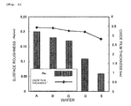
The thus prepared semiconductor silicon wafers were subjected to polishing and others to provide wafers on 5 standards (A, B, C, D and E) having different surface roughness values obtained by measurement using an AFM. These semiconductor silicon wafers were placed on a boat to be put into a vertical heat treating furnace, a film thickness of 3 nm was determined as a target, and a heat treatment was performed at 800° C., in a dry oxygen atmosphere (an oxygen partial pressure of 0.1 atom: diluted oxidation) to form an oxide film on each wafer main surface. Then, an ellipsometer (λ=633 nm) was utilized to measure an oxide film thickness on each wafer (A, B, C, D or E). FIG. 1 shows a relationship between this oxide film thickness and the surface roughness.
As apparent from FIG. 1, it can be understood that a thickness of the oxide film is small (an oxidation rate is low) as the surface roughness is small (as the surface is flat). Therefore, it can be also understood that using such a measurement result enables adjusting oxidizing conditions.
A surface layer portion of each of these semiconductor silicon wafers (A, B, C, D and E) before a heat treatment was subjected to In-plane diffraction (see FIG. 2) as X-ray diffraction measurement to obtain a rocking curve, and its full width at half maximum was measured. FIG. 3 shows a relationship between the full width at half maximum and the surface roughness at this time.
As apparent from FIG. 3, it can be understood that the surface roughness and crystallinity have a close correlation, and both of them can be measured to be used as oxidation rate parameters.
Then, these semiconductor wafers (A, B, C, D and E) were placed on the boat and put into the vertical heat treating furnace, each oxide film was further formed by dry oxidation at 800° C. until reaching a thickness of 5 nm, thereby forming each gate oxide film.
Subsequently, these semiconductor wafers (A, B, C, D and E) were put into a CVD furnace, and a polysilicon layer was grown on each gate oxide film while doping phosphorus. A thickness of the grown polysilicon layer was approximately 300 nm, and a resistance value was approximately 25 Ω/sq in terms of sheet resistance.
Then, these semiconductor silicon wafers (A, B, C, D and E) were subjected to patterning using a photolithography technology and polysilicon layer removal based on etching, and 100 MOS capacitors using the polysilicon layer as an electrode were fabricated within each semiconductor silicon wafer plane. It is to be noted that, as polysilicon etching after photolithography, wet etching using a hydrofluoric-nitric acid was performed. At last, to remove the silicon oxide film formed on each semiconductor silicon wafer back surface, a resist was applied to each semiconductor silicon wafer main surface, and wet etching using a diluted hydrofluoric acid was carried out to remove the silicon oxide film on the wafer back surface.
An electric field stress was applied to the gate oxide film by using a constant-current TDDB method for applying a constant current to each processed semiconductor wafer (A, B, C, D or E) until the gate oxide film is destroyed. The applied current stress was 0.001 A/cm2, and a measurement temperature was set to 100° C. while considering a reduction in measurement time. A tester connected to a fully-automatic prober was used for the measurement. An electrode area in this example was 4 mm2. FIG. 4 shows a measurement result as a Weibull plot.
FIG. 4 is called the Weibull plot and it is often used when describing a semiconductor device failure distribution such as TDDB. Its abscissa represents a charge amount Qbd (C/cm2) applied to the oxide film as an index while its ordinate represents lnln (1/(1−F(t))). Here, F(t) represents a cumulative failure rate and, for example, a Weibull value when the cumulative failure rate is 50% is −0.37.
As can be seen from FIG. 4, degradation in TDDB characteristics (a reduction in reliability) was observed in the wafers A and B each having Ra equal to or above 0.18 nm and a full width at half maximum higher than 0.00074°. As a result, it can be understood that a degree of degradation in TDDB characteristics is small in a silicon wafer having Ra of 0.17 nm or below and a full width at half maximum of 0.00074° or below. That is considered to be because an oxidation rate is sufficiently low and control over an oxide film thickness is easy in such a silicon wafer, an accurate film thickness can be thus obtained, and the oxidation rate is relatively uniform within a wafer plane, whereby film thickness uniformity of the oxide film is high.
It is to be noted that the present invention is not restricted to the foregoing embodiment. The embodiment is just an exemplification, and any examples that have substantially the same configuration and demonstrate the same functions and effects as the technical concept described in claims of the present invention are included in the technical scope of the present invention.

Claims (19)

1. A method for forming an oxide film on a silicon wafer, comprising: measuring surface roughness of the silicon wafer and/or crystallinity in a surface layer portion of the silicon wafer to obtain at least one measurement value; after the measuring, adjusting oxidizing conditions for the silicon wafer based on the at least one measurement value; and forming the oxide film on the silicon wafer under the adjusted oxidizing conditions.
2. The method for forming an oxide film on a silicon wafer according to claim 1, wherein the surface roughness of the silicon wafer is measured by using an AFM to measure an Ra value of the surface roughness of the silicon wafer.
3. The method for forming an oxide film on a silicon wafer according to claim 2, wherein the oxidizing conditions for the silicon wafer are adjusted based on whether the measured Ra value of the surface roughness is not more than 0.17 nm.
4. The method for forming an oxide film on a silicon wafer according to claim 1, wherein the crystallinity in the surface layer portion of the silicon wafer is measured by measuring a full width at half maximum of a rocking curve obtained by X-ray diffraction measurement.
5. The method for forming an oxide film on a silicon wafer according to claim 2, wherein the crystallinity in the surface layer portion of the silicon wafer is measured by measuring a full width at half maximum of a rocking curve obtained by X-ray diffraction measurement.
6. The method for forming an oxide film on a silicon wafer according to claim 3, wherein the crystallinity in the surface layer portion of the silicon wafer is measured by measuring a full width at half maximum of a rocking curve obtained by X-ray diffraction measurement.
7. The method for forming an oxide film on a silicon wafer according to claim 4, wherein the oxidizing conditions for the silicon wafer are adjusted based on whether the measured full width at half maximum of the rocking curve is not more than 0.00074°.
8. The method for forming an oxide film on a silicon wafer according to claim 5, wherein the oxidizing conditions for the silicon wafer are adjusted based on whether the measured full width at half maximum of the rocking curve is not more than 0.00074°.
9. The method for forming an oxide film on a silicon wafer according to claim 6, wherein the oxidizing conditions for the silicon wafer are adjusted based on whether the measured full width at half maximum of the rocking curve is not more than 0.00074°.
10. The method for forming an oxide film on a silicon wafer according to claim 1, wherein a thickness of the oxide film to be formed is set to 5 nm or below.
11. The method for forming an oxide film on a silicon wafer according to claim 2, wherein a thickness of the oxide film to be formed is set to 5 nm or below.
12. The method for forming an oxide film on a silicon wafer according to claim 3, wherein a thickness of the oxide film to be formed is set to 5 nm or below.
13. The method for forming an oxide film on a silicon wafer according to claim 4, wherein a thickness of the oxide film to be formed is set to 5 nm or below.
14. The method for forming an oxide film on a silicon wafer according to claim 5, wherein a thickness of the oxide film to be formed is set to 5 nm or below.
15. The method for forming an oxide film on a silicon wafer according to claim 6, wherein a thickness of the oxide film to be formed is set to 5 nm or below.
16. The method for forming an oxide film on a silicon wafer according to claim 7, wherein a thickness of the oxide film to be formed is set to 5 nm or below.
17. The method for forming an oxide film on a silicon wafer according to claim 8, wherein a thickness of the oxide film to be formed is set to 5 nm or below.
18. The method for forming an oxide film on a silicon wafer according to claim 9, wherein a thickness of the oxide film to be formed is set to 5 nm or below.
19. The method for forming an oxide film on a silicon wafer according to claim 1, wherein the oxidizing conditions for the silicon wafer are adjusted by at least one of:
an oxidation time,
an oxidation temperature and
sorting each silicon wafer on which the oxide film is to be formed together.
US12/921,492 2008-04-25 2009-03-24 Method for forming oxide film on silicon wafer Active US8043871B2 (en)

Applications Claiming Priority (3)

Application Number Priority Date Filing Date Title
JP2008-115672 2008-04-25
JP2008115672A JP5272496B2 (en) 2008-04-25 2008-04-25 Method for forming oxide film on silicon wafer
PCT/JP2009/001281 WO2009130847A1 (en) 2008-04-25 2009-03-24 Method for formation of oxide film for silicon wafer

Publications (2)

Publication Number Publication Date
US20110033958A1 US20110033958A1 (en) 2011-02-10
US8043871B2 true US8043871B2 (en) 2011-10-25

Family

ID=41216590

Family Applications (1)

Application Number Title Priority Date Filing Date
US12/921,492 Active US8043871B2 (en) 2008-04-25 2009-03-24 Method for forming oxide film on silicon wafer

Country Status (6)

Country Link
US (1) US8043871B2 (en)
EP (1) EP2273539B1 (en)
JP (1) JP5272496B2 (en)
KR (1) KR101559985B1 (en)
CN (1) CN102017098B (en)
WO (1) WO2009130847A1 (en)

Cited By (1)

* Cited by examiner, † Cited by third party
Publication number Priority date Publication date Assignee Title
US10580874B2 (en) * 2017-02-09 2020-03-03 Kabushiki Kaisha Toshiba Semiconductor device with silicon oxide layer having element double bonded to oxygen, semiconductor device manufacturing method, inverter circuit, driving device, vehicle, and elevator

Families Citing this family (8)

* Cited by examiner, † Cited by third party
Publication number Priority date Publication date Assignee Title
US8921992B2 (en) 2013-03-14 2014-12-30 Raytheon Company Stacked wafer with coolant channels
US9842762B1 (en) * 2016-11-11 2017-12-12 Globalfoundries Inc. Method of manufacturing a semiconductor wafer having an SOI configuration
KR102014926B1 (en) * 2017-10-31 2019-08-27 에스케이실트론 주식회사 Method for predicting thickness of oxide layer of silicon wafer
CN108054112B (en) * 2017-12-21 2021-11-30 重庆超硅半导体有限公司 Method for testing minority carrier lifetime of IC-level silicon wafer
KR102094153B1 (en) * 2018-10-16 2020-03-27 한국표준과학연구원 Method for Forming High-k Insulating Film of MOS Transistor
CN111106027A (en) * 2019-12-23 2020-05-05 武汉大学 Measurement modification system for SOI top silicon wafer
CN112857270B (en) * 2021-01-08 2022-12-09 上海科技大学 Method for in-situ real-time quantitative detection of film roughness by using RHEED
JP2023069889A (en) * 2021-11-08 2023-05-18 信越半導体株式会社 Film thickness evaluation method of oxide film and manufacturing method of silicon substrate with the oxide film

Citations (4)

* Cited by examiner, † Cited by third party
Publication number Priority date Publication date Assignee Title
JPH0513395A (en) 1991-07-02 1993-01-22 Tadahiro Omi Silicon wafer and cleaning method
JPH1079376A (en) 1996-08-05 1998-03-24 Texas Instr Inc <Ti> Method of depositing thin film on single crystalline semiconductor substrate
US20070145535A1 (en) * 2002-12-02 2007-06-28 Foundation For Advancement Of International Science Semiconductor device and method of manufacturing the same
US20080187768A1 (en) * 2005-03-11 2008-08-07 The Arizona Board Of Regents Novel Gesisn-Based Compounds, Templates, and Semiconductor Structures

Family Cites Families (2)

* Cited by examiner, † Cited by third party
Publication number Priority date Publication date Assignee Title
JP3417665B2 (en) * 1994-07-07 2003-06-16 株式会社東芝 Method for manufacturing semiconductor device
US6723666B1 (en) * 2003-03-06 2004-04-20 Advanced Micro Devices, Inc. Method for reducing gate oxide surface irregularities

Patent Citations (6)

* Cited by examiner, † Cited by third party
Publication number Priority date Publication date Assignee Title
JPH0513395A (en) 1991-07-02 1993-01-22 Tadahiro Omi Silicon wafer and cleaning method
EP0592671A1 (en) 1991-07-02 1994-04-20 OHMI, Tadahiro Silicon wafer and its cleaning method
JPH1079376A (en) 1996-08-05 1998-03-24 Texas Instr Inc <Ti> Method of depositing thin film on single crystalline semiconductor substrate
US6020247A (en) 1996-08-05 2000-02-01 Texas Instruments Incorporated Method for thin film deposition on single-crystal semiconductor substrates
US20070145535A1 (en) * 2002-12-02 2007-06-28 Foundation For Advancement Of International Science Semiconductor device and method of manufacturing the same
US20080187768A1 (en) * 2005-03-11 2008-08-07 The Arizona Board Of Regents Novel Gesisn-Based Compounds, Templates, and Semiconductor Structures

Non-Patent Citations (12)

* Cited by examiner, † Cited by third party
Title
Choi et al., "Anomalous oxidation rate of silicon implanted with very high doses of arsenic," Appl. Phys. Lett., vol. 51, No. 13, pp. 1001-1003, 1987.
Deal et al., "Thermal Oxidation of Heavily Doped Silicon," Journal of the Electrochemical Society, vol. 112, No. 4, pp. 430-435, 1965.
Deal, "Thermal Oxidation Kinetics of Silicon in Pyrogenic H2O and 5% HCI/H2O Mixtures," Journal of the Electrochemical Society: Solid-State Science Technology, vol. 125, No. 4, pp. 576-579, 1978.
Ho et al., "Si/SiO2 Interface Oxidation Kinetics: A Physical Model for the Influence of High Substrate Doping Levels, I, Theory," Journal of the Electrochemical Society: Solid-State Science and Technology, vol. 126, No. 9, pp. 1516-1522, 1979.
Ho et al., "Si/SiO2 Interface Oxidation Kinetics: A Physical Model for the Influence of High Substrate Doping Levels, II. Comparison with Experiment and Discussion," Journal of the Electrochemical Society: Solid-State Science and Technology, vol. 126, No. 9, pp. 1523-1530, 1979.
Ho et al., "Thermal Oxidation of Heavily Phosphorus-Doped Silicon," Journal of the Electrochemical Society: Solid-State Science and Technology, vol. 125, No. 4, pp. 665-671, 1978.
International Preliminary Report on Patentability issued in International Patent Application No. PCT/JP2009/001281 dated Dec. 13, 2010.
International Search Report issued in International Application No. PCT/JP2009/001281 dated Jun. 16, 2009.
Irene et al., "Silicon Oxidation Studies: Silicon Orientation Effects on Thermal Oxidation," Journal of the Electrochemical Society: Solid-State Science and Technology, vol. 133, No. 6, pp. 1253-1256, 1986.
Raider et al., "Reversal of Relative Oxidation Rates of <111> and <100> Oriented Silicon Substrates at Low Oxygen Partial Pressures," Journal of the Electrochemical Society: Solid-State Science and Technology, vol. 127, No. 8, pp. 1783-1787, 1980.
Raider et al., "Reversal of Relative Oxidation Rates of and Oriented Silicon Substrates at Low Oxygen Partial Pressures," Journal of the Electrochemical Society: Solid-State Science and Technology, vol. 127, No. 8, pp. 1783-1787, 1980.
Takakuwa, "Growth Kinetics of Very Thin Oxide Layers on Si(001) Surface Monitored in Real-time by Auger Electron Spectroscopy Combined with Reflection High Energy Electron Diffraction," Surface Science, vol. 23, No. 9, pp. 536-552, 2002 (with abstract).

Cited By (1)

* Cited by examiner, † Cited by third party
Publication number Priority date Publication date Assignee Title
US10580874B2 (en) * 2017-02-09 2020-03-03 Kabushiki Kaisha Toshiba Semiconductor device with silicon oxide layer having element double bonded to oxygen, semiconductor device manufacturing method, inverter circuit, driving device, vehicle, and elevator

Also Published As

Publication number Publication date
US20110033958A1 (en) 2011-02-10
JP2009267125A (en) 2009-11-12
EP2273539B1 (en) 2017-06-28
KR20110014978A (en) 2011-02-14
WO2009130847A1 (en) 2009-10-29
EP2273539A4 (en) 2013-03-27
KR101559985B1 (en) 2015-10-13
CN102017098B (en) 2013-01-30
JP5272496B2 (en) 2013-08-28
CN102017098A (en) 2011-04-13
EP2273539A1 (en) 2011-01-12

Similar Documents

Publication Publication Date Title
US8043871B2 (en) Method for forming oxide film on silicon wafer
US7103484B1 (en) Non-contact methods for measuring electrical thickness and determining nitrogen content of insulating films
Nieh et al. Electrical characterization and material evaluation of zirconium oxynitride gate dielectric in TaN-gated NMOSFETs with high-temperature forming gas annealing
US6465265B2 (en) Analysis of interface layer characteristics
US20220146444A1 (en) Method for measuring resistivity of silicon single crystal
US7745236B2 (en) Floating gate process methodology
Miura et al. Effect of mechanical stress on reliability of gate-oxide film in MOS transistors
JP6451881B1 (en) Silicon layer evaluation method and silicon epitaxial wafer manufacturing method
US6821892B1 (en) Intelligent wet etching tool as a function of chemical concentration, temperature and film loss
Choi et al. Cleaning of Si and properties of the HfO 2–Si interface
JP2010050353A (en) Semiconductor wafer, method of manufacturing the same, and method of evaluating the same
CN114284168B (en) Method for measuring silicon oxynitride gate dielectric layer and method for manufacturing semiconductor device
Chao et al. Multiple‐Angle Incident Ellipsometry Measurement on Low Pressure Chemical Vapor Deposited Amorphous Silicon and Polysilicon
JP5217353B2 (en) Insulating film formation method
JP5729098B2 (en) Evaluation method of silicon single crystal wafer
CN114068343B (en) Method for monitoring thickness of gate dielectric layer
Hoff Growth and metrology of silicon oxides on silicon carbide
Misra et al. Metal-oxide-silicon diodes on deuterium-implanted silicon substrate
US20030001243A1 (en) Method of monitoring ultra-thin nitride quality by wet re-oxidation
TW493237B (en) Quality monitoring method of ultra thin silicon nitride film
JP2001274214A (en) Method for evaluating semiconductor silicon wafer and method for controlling manufacturing process
Tallarida et al. Surface morphology of nitrided thin thermal SiO2 studied by atomic force microscopy
Edrei et al. Silicon nano-asperities: Morphological evolution and electrical properties of double-polysilicon interlayers
Tyaginov et al. Determination of correlation length for thickness fluctuations in thin oxide and fluoride films
Wostyn et al. HF-Last Wet Clean in Combination with a Low Temperature GeH4-Assisted HCl In Situ Clean Prior to Si0. 8Ge0. 2-on-Si Epitaxial Growth

Legal Events

Date Code Title Description
AS Assignment

Owner name: SHIN-ETSU HANDOTAI CO., LTD., JAPAN

Free format text: ASSIGNMENT OF ASSIGNORS INTEREST;ASSIGNORS:OHTSUKI, TSUYOSHI;TOBE, SATOSHI;MIZUSAWA, YASUSHI;REEL/FRAME:024958/0047

Effective date: 20100810

STCF Information on status: patent grant

Free format text: PATENTED CASE

FEPP Fee payment procedure

Free format text: PAYOR NUMBER ASSIGNED (ORIGINAL EVENT CODE: ASPN); ENTITY STATUS OF PATENT OWNER: LARGE ENTITY

FPAY Fee payment

Year of fee payment: 4

MAFP Maintenance fee payment

Free format text: PAYMENT OF MAINTENANCE FEE, 8TH YEAR, LARGE ENTITY (ORIGINAL EVENT CODE: M1552); ENTITY STATUS OF PATENT OWNER: LARGE ENTITY

Year of fee payment: 8

MAFP Maintenance fee payment

Free format text: PAYMENT OF MAINTENANCE FEE, 12TH YEAR, LARGE ENTITY (ORIGINAL EVENT CODE: M1553); ENTITY STATUS OF PATENT OWNER: LARGE ENTITY

Year of fee payment: 12