EP0588635A1 - Speisespannungsschaltung für Gatesteuerstufe - Google Patents
Speisespannungsschaltung für Gatesteuerstufe Download PDFInfo
- Publication number
- EP0588635A1 EP0588635A1 EP93307312A EP93307312A EP0588635A1 EP 0588635 A1 EP0588635 A1 EP 0588635A1 EP 93307312 A EP93307312 A EP 93307312A EP 93307312 A EP93307312 A EP 93307312A EP 0588635 A1 EP0588635 A1 EP 0588635A1
- Authority
- EP
- European Patent Office
- Prior art keywords
- capacitor
- diode
- gate
- snubber
- terminal
- Prior art date
- Legal status (The legal status is an assumption and is not a legal conclusion. Google has not performed a legal analysis and makes no representation as to the accuracy of the status listed.)
- Granted
Links
- 239000003990 capacitor Substances 0.000 claims abstract description 127
- 230000008929 regeneration Effects 0.000 claims description 6
- 238000011069 regeneration method Methods 0.000 claims description 6
- 238000010586 diagram Methods 0.000 description 14
- 230000009471 action Effects 0.000 description 6
- 230000003287 optical effect Effects 0.000 description 3
- 230000000087 stabilizing effect Effects 0.000 description 3
- 238000013459 approach Methods 0.000 description 2
- 230000008901 benefit Effects 0.000 description 2
- 230000009467 reduction Effects 0.000 description 2
- 230000001172 regenerating effect Effects 0.000 description 2
- 230000003321 amplification Effects 0.000 description 1
- 230000009286 beneficial effect Effects 0.000 description 1
- 238000010276 construction Methods 0.000 description 1
- 238000001514 detection method Methods 0.000 description 1
- 230000006872 improvement Effects 0.000 description 1
- 238000004519 manufacturing process Methods 0.000 description 1
- 238000000034 method Methods 0.000 description 1
- 238000012986 modification Methods 0.000 description 1
- 230000004048 modification Effects 0.000 description 1
- 238000003199 nucleic acid amplification method Methods 0.000 description 1
- 239000013307 optical fiber Substances 0.000 description 1
- 108091008695 photoreceptors Proteins 0.000 description 1
- 230000001629 suppression Effects 0.000 description 1
Images


Classifications
-
- H—ELECTRICITY
- H02—GENERATION; CONVERSION OR DISTRIBUTION OF ELECTRIC POWER
- H02M—APPARATUS FOR CONVERSION BETWEEN AC AND AC, BETWEEN AC AND DC, OR BETWEEN DC AND DC, AND FOR USE WITH MAINS OR SIMILAR POWER SUPPLY SYSTEMS; CONVERSION OF DC OR AC INPUT POWER INTO SURGE OUTPUT POWER; CONTROL OR REGULATION THEREOF
- H02M1/00—Details of apparatus for conversion
- H02M1/08—Circuits specially adapted for the generation of control voltages for semiconductor devices incorporated in static converters
-
- H—ELECTRICITY
- H03—ELECTRONIC CIRCUITRY
- H03K—PULSE TECHNIQUE
- H03K17/00—Electronic switching or gating, i.e. not by contact-making and –breaking
- H03K17/08—Modifications for protecting switching circuit against overcurrent or overvoltage
- H03K17/081—Modifications for protecting switching circuit against overcurrent or overvoltage without feedback from the output circuit to the control circuit
- H03K17/0814—Modifications for protecting switching circuit against overcurrent or overvoltage without feedback from the output circuit to the control circuit by measures taken in the output circuit
- H03K17/08144—Modifications for protecting switching circuit against overcurrent or overvoltage without feedback from the output circuit to the control circuit by measures taken in the output circuit in thyristor switches
-
- H—ELECTRICITY
- H03—ELECTRONIC CIRCUITRY
- H03K—PULSE TECHNIQUE
- H03K17/00—Electronic switching or gating, i.e. not by contact-making and –breaking
- H03K17/10—Modifications for increasing the maximum permissible switched voltage
- H03K17/105—Modifications for increasing the maximum permissible switched voltage in thyristor switches
Definitions
- This invention relates to a gate power supply circuit, and more particularly embodiments relate to a gate power supply circuit that supplies gate power to the gate drive circuit for a self-turn-off device from a main circuit, utilizing the switching action of a self-turn-off device etc.
- the gate drive circuit of a GTO Since the gate drive circuit of a GTO is directly connected to the cathode and gate of the GTO that is being driven, it is electrically at the same potential as the cathode of the GTO that is being driven.
- the gate drive circuit of each GTO When GTOs are connected in series, the gate drive circuit of each GTO is at a respectively different potential, so the power sources of the respective gate drive circuits must be at respectively different potentials. This means that the power sources of the gate drive circuits of the GTOs must be mutually insulated for each respective GTO.
- FIG. 9 shows a single GTO of a plurality of GTOs constituting a power converter and the associated snubber circuit and gate drive circuit.
- a GTO 1 is the main switching device.
- a snubber diode 2 and a snubber capacitor 3 constitute a snubber circuit for suppressing the rate of voltage rise when GTO 1 is turned OFF, and suppress GTO loss on turn-off.
- a resistor 4 dissipates the energy stored in snubber capacitor 3.
- a diode 5 is a free-wheeling diode that provides a current path for the main circuit current in regeneration mode.
- a resistor 6 is a DC balance resistor that performs the action of balancing the DC voltages apportioned to each GTO when a large number of GTOs are connected in series, so that they are not affected by the slight variations of the characteristics of each GTO.
- the gate of GTO 1 is driven by a gate drive circuit 7.
- the ON/OFF signal of the gate is transmitted as an optical signal by an optical fiber 8 and is converted to an electrical signal by a photoreceptor module, not shown, in gate drive circuit 7. Since an optical signal is employed, the ON/OFF gate signals are automatically insulated for each GTO 1.
- this can be obtained by using a rectifier 9 to produce DC power by rectifying the high frequency (such as 20 kHz) AC power supplied from a high frequency AC power source 11 through an isolating transformer 10.
- High frequency AC power source 11 is located in a low potential zone and is supplied in common to each GTO; the difference in potential between GTOs 1 is insulated by means of isolating transformer 10 corresponding to each respective GTO 1.
- one object of this invention is to provide a gate power supply circuit which can dispense with an isolating transformer and facilitates minaturization and cost reduction of a power converter constructed using self-turn-off devices.
- a gate power supply circuit including a switching device and a gate drive circuit connected to the switching device for generating a gate signal to be supplied to a gate of the switching device.
- the gate power supply circuit further includes a series circuit of a snubber capacitor and a snubber diode connected in parallel with the switching device, and an inductor, a first terminal of which is connected to a connection point of the switching device and the snubber diode.
- the gate power supply circuit also includes a series circuit of power disposing circuit and a first diode, connected between a series connection point of the snubber capacitor and the snubber diode and a second terminal of the inductor.
- the gate power supply circuit further includes a series circuit of a power supplying capacitor and a second diode, connected in parallel with the inductor.
- the gate drive circuit is connected to the power supplying capacitor to receive energy stored in the power supplying capacitor as power source for the gate drive circuit.
- a gate power supply circuit including a plurality of valve units, an inductor having a first terminal and a second terminal and a power disposing circuit. A first terminal of the power disposing circuit is connected to the second terminal of the inductor.
- Each of the valve units includes a switching device, a gate drive circuit connected to the switching device for generating a gate signal to be supplied to a gate of the switching device, a series circuit of a snubber capacitor and a snubber diode connected in parallel with the switching device, a first diode, a first terminal of which being connected to a series connection point of the snubber capacitor and the snubber diode, and a series circuit of a power supplying capacitor and a second diode.
- a first terminal of the power supplying capacitor is connected to a connection point of the switching device and the snubber diode, and a second terminal of the power supplying capacitor is connected to a first terminal of the second diode.
- the gate drive circuit is connected to the power supplying capacitor to receive energy stored in the power supplying capacitor as power source for the gate drive circuit.
- a plurality of the valve units and the inductor are connected in series, such that a plurality of the switching devices are connected in series, and the inductor is connected in series with the series connected switching devices such that the first terminal of the inductor is connected to the connection point of the switching device and the snubber diode of the valve unit in a last stage.
- a second terminal of the first diode of the valve unit in a stage except the last stage is connected to the first terminal of the first diode of the valve unit in a next stage, and a second terminal of the first diode of the valve unit in the last stage is connected to a second terminal of the power disposing circuit.
- a second terminal of the second diode of the valve unit in the stage except the last stage is connected to the first terminal of the second diode of the valve unit in the next stage, and a second terminal of the second diode of the valve unit in the last stage is connected to a second terminal of the inductor.
- the gate power supply circuit is so arranged that power supplied to the gate drive circuit is obtained from the main circuit by utilizing ON/OFF action of the self-turn-off device, to dispense with an isolating transformer.
- Fig. 1 is a layout diagram showing a gate power supply circuit according to a first embodiment of this invention.
- 1 is a self-turn-off device (hereinbelow referred to as GTO 1) of the main circuit.
- GTO 1 a self-turn-off device
- a snubber circuit consisting of the series circuit of a snubber diode 2 and snubber capacitor 3, a free-wheeling diode 5 and a DC balance resistor 6 are connected in parallel with GTO 1.
- One terminal of an inductor 12 is connected to the cathode side of GTO 1, while a series circuit consisting of a first diode 15 and a first capacitor 16 is connected between the other terminal of inductor 12 and the series connection point of snubber diode 2 and snubber capacitor 3, and a resistor 17 is connected in parallel with capacitor 16. Furthermore, a series circuit consisting of a power supplying capacitor, such as a second capacitor 13, and a second diode 14 is connected in parallel with inductor 12, so that the energy stored in second capacitor 13 is fed to gate drive circuit 7.
- VAK is a voltage between an anode and a cathode of GTO 1
- VC13 is a voltage of second capacitor 13
- ID14 is a current flowing through second diode 14
- VL12 is a voltage of inductor 12.
- snubber capacitor 3 Whilst GTO 1 is OFF, snubber capacitor 3 is charged through snubber diode 2 and inductor 12 practically up to the DC apportioned voltage VAK of GTO 1.
- GTO 1 is turned ON and voltage VAK of GTO 1 drops.
- first diode 15 conducts, and the charge of snubber capacitor 3 is discharged by the loop: GTO 1 ⁇ inductor 12 ⁇ first capacitor 16 ⁇ first diode 15. Since the voltage VAK of GTO 1 rapidly approaches zero, voltage VL12 of inductor 12 becomes directly that of snubber capacitor 3. Discharge of snubber capacitor 3 terminates at time point B.
- inductor 12 After time point B, the current of inductor 12 flows in the first loop: inductor 12 ⁇ first capacitor 16 ⁇ first diode 15 ⁇ snubber diode 2 ⁇ inductor 12, and in the second loop: inductor 12 ⁇ second diode 14 ⁇ second capacitor 13 ⁇ inductor 12. Thereby, second capacitor 13 is charged, and the voltage VC13 of second capacitor 13 rises.
- the snubber energy that has been transferred to inductor 12 has all completed its transfer to first capacitor 16 and second capacitor 13.
- the energy stored in first capacitor 16 is dissipated by resistor 17 and the energy stored in second capacitor 13 is supplied to gate drive circuit 7.
- first capacitor 16 of sufficiently large capacity the voltage of first capacitor 16 always maintains a practically constant voltage level. Since the charged voltage of second capacitor 13 is equal to the voltage of first capacitor 16, if the value of first capacitor 16 is made sufficiently large, every time GTO 1 is turned ON, the voltage of second capacitor 13 will be charged up to a fixed voltage equal to the voltage of first capacitor 16. In this case, the voltage of first capacitor 16 is determined by the value of resistor 17 and the input power to first capacitor 16 that is determined by the switching frequency of GTO 1 and the energy stored in snubber capacitor 3 during the period while GTO 1 is OFF.
- the energy stored in the power supplying capacitor, such as second capacitor 13, is supplied to gate drive circuit 7, so that an isolating transformer capable of withstanding high voltage that is necessary in the prior art shown in Fig. 9 can be omitted.
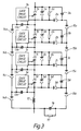
- Fig. 3 is a layout diagram showing a gate power supply circuit according to a second embodiment of this invention.
- a single switching valve is constituted by connecting in series four GTOs 1a, 1b, 1c and 1d that are driven by the same gate signal.
- suffixs a, b, c and d are attached to reference numerals indicating components in valve units a, b, c and d constituting a single switching valve, respectively.
- the arm of a power converter is constituted by further connecting a large number of the switching valves thereby obtained in series.
- the rate of current rise of the GTO is suppressed by a single anode inductor 12 provided in a single switching valve. Even in the case of the gate power supply circuit of this invention, a single anode inductor 12 is used in common with four gate supply circuits.
- GTOs 1a to 1d turn ON, and the voltages VAK of GTOs 1a to 1d drop.
- first diodes 15a to 15d conduct.
- the charge of snubber capacitor 3d starts to be discharged by the loop: snubber capacitor 3d ⁇ GTO 1d ⁇ inductor 12 ⁇ first capacitor 16 ⁇ first diode 15d ⁇ snubber capacitor 3d.
- the charge of snubber capacitor 3c is discharged by the loop: snubber capacitor 3c ⁇ GTO 1c ⁇ GTO 1d ⁇ inductor 12 ⁇ first capacitor 16 ⁇ first diode 15d ⁇ first diode 15c ⁇ first snubber capacitor 3c.
- the charge of snubber capacitor 3b is discharged by the loop: snubber capacitor 3b ⁇ GTO 1b ⁇ GTO 1c ⁇ GTO 1d ⁇ inductor 12 ⁇ first capacitor 16 ⁇ first diode 15d ⁇ first diode 15c ⁇ first diode 15b ⁇ snubber capacitor 3b.
- snubber capacitor 3a ⁇ GTO 1a ⁇ GTO 1b ⁇ GTO 1c ⁇ GTO 1d ⁇ inductor 12 ⁇ first capacitor 16 ⁇ first diode 15d ⁇ first diode 15c ⁇ first diode 15b ⁇ first diode 15a ⁇ snubber capacitor 3a. Since voltages VAK of GTOs 1a to 1d rapidly approach zero, voltage VL12 of inductor 12 becomes the same as the voltage of snubber capacitors 3a to 3d which have become equivalently connected in parallel. Discharge of snubber capacitor 3a to 3d ceases at time point B.
- inductor 12 After time point B, the current of inductor 12 flows in the loops: inductor 12 ⁇ first capacitor 16 ⁇ first diode 15d ⁇ snubber diode 2d ⁇ inductor 12.
- the current of inductor 12 flows also in the loop d: inductor 12 ⁇ second diode 14d ⁇ second capacitor 13d ⁇ inductor 12; furthermore, it flows in the loop c: inductor 12 ⁇ second diode 14d ⁇ second diode 14c ⁇ second capacitor 13c ⁇ GTO 1d ⁇ inductor 12, in the loop b: inductor 12 ⁇ second diode 14d ⁇ second diode 14c ⁇ second diode 14b ⁇ second capacitor 13b ⁇ GTO 1c ⁇ GTO 1d ⁇ inductor 12, and in the loop a: inductor 12 ⁇ second diode 14d ⁇ second diode 14c ⁇ second diode 14b ⁇ second disode 14a ⁇ second capacitor 13
- second diode 14a there flows the current that charges second capacitor 13a and, in second diode 14b, in addition to the current that charges second capacitor 13b, there flows the current that charges second capacitor 13a.
- second diode 14c there flows the currents that charge second capacitors 13c, 13b and 13a, respectively
- second diode 14d there flows the currents that charge second capacitors 13d, 13c, 13b and 13a, respectively. Consequently, as shown in Fig. 4, as one goes down through the four series-connected second diodes 14a to 14d, it will be found that these are passing progressively more currents ID14a to ID14d.
- Second capacitors 13a to 13d are thereby charged, and the respective voltages VC13a, VC13b, VC13c and VC13d of second capacitors 13a to 13d rise.
- the energy stored in first capacitor 16 is dissipated by resistor 17, and the energies stored in second capacitors 13a to 13d are respectively fed to gate drive circuits 7a to 7d.
- the number of GTOs in Fig. 3 is four, but there is no restriction to four, and the arrangement can be put into practice with any number of GTOs connected in series.
- first capacitor 16 the energy stored in first capacitor 16 was dissipated by resistor 17.
- resistor 17 This layout involves only a small number of components, but in particular in high voltage applications, results in considerable losses, lowering efficiency as a power converter.
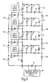
- the third embodiment of this invention shown in Fig. 5 may be employed.
- resistor 17 instead of resistor 17, use is made of a chopper or DC/DC converter or the like, so that the energy stored in first capacitor 16 can be regenerated.
- a snubber energy regeneration circuit 18 constituted by a chopper or DC/DC converter or the like.
- the construction of the snubber energy regeneration circuit 18 is well known to those skilled it the art, so that the detailed description thereof may by omitted.
- the rest of the layout is the same as Fig. 3.
- the operation of this third embodiment therefore differs only in that the energy stored in first capacitor 16 is regenerated at the power source side of load side by snubber energy regenerating circuits 18. With such a layout, the voltage of first capacitor 16 is controlled by the action of snubber energy regenerating circuit 18 such as to be a fixed voltage.
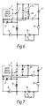
- Fig. 6 is a layout diagram showing a gate power supply circuit according to a fourth embodiment of this invention adapted for such cases.
- a voltage dividing-circuit consisting of voltage-dividing resistors 6a and 6b connected in series is connected in parallel with GTO 1, so that second capacitor 13 is charged during the OFF period of GTO 1.
- GTO 1 the voltage-dividing circuit
- voltage-dividing resistors 6a and 6b also perform the role of balance resistor of GTO 1.
- Fig. 7 is a layout diagram showing a gate power supply circuit according to a fifth embodiment of this invention for use in such a case.
- the current that flows through resistor 6c before GTO 1 starts switching constitutes the power source of gate drive circuit 7.
- a suitable voltage stabilizing means must be incorporated on the side of the gate drive circuit 7, but this can easily be implemented and need not therefore be shown as a practical example.
- first capacitor 16 of the embodiment of Fig. 1 is not necessarily essential. The reason for this is that first capacitor 16 serves for receiving the energy stored in inductor 12; once it has been received in first capacitor 16, it is dissipated by resistor 17 or it should be regenerated by a DC/DC converter or the like; there is therefore no problem in allowing the energy to be directly dissipated by resistor 17 without passing through first capacitor 16.
- Fig. 8 is a layout diagram showing a gate power supply circuit according to a sixth embodiment of this invention based on this concept.
- the embodiment of Fig. 8 is characterized in that, compared with the embodiment of Fig. 1, first capacitor 16 is not provided and the energy is directly dissipated by resistor 17. As already mentioned, the larger first capacitor 16 is made, the more stable will its voltage be, so if on the other hand first capacitor 16 is absent, there will be considerable fluctuation of the source voltage of gate drive circuit 7. However, this can be allowed, due to the provision of voltage stabilizing means within gate drive circuit 7.
- the sixth embodiment is particularly beneficial where, in the case of a low-snubber GTO with small capacity of snubber capacitor 3, there is no energy worth returning for regeneration, so first capacitor 16 is omitted and resistor 17 can be provided.
- gate drive circuit therefore includes, the circuits to which this invention could be applied, for example, fault detection circuits with switching devices attached, or control and protection circuits etc. for high potential units. In this invention, these are designated by the general term "gate drive circuit or the like".
- the gate power supply circuit As described above, with the gate power supply circuit according to this invention, energy is obtained from the main circuit side utilizing the switching action of switching devices located in the main circuit, so the energy stored in the snubber capacitor during the off period of the switching device is transferred to a power supplying capacitor, such as a second capacitor, through an inductor during the ON period of the switching device, thereby enabling the energy stored in this second capacitor to be utilized; the large number of isolating transformers of high withstand voltage that were necessary in the prior art are thereby made unnecessary, enabling miniaturization and cost reduction of a power converter constructed using self-turn-off devices.
- a power supplying capacitor such as a second capacitor
Landscapes
- Engineering & Computer Science (AREA)
- Power Engineering (AREA)
- Power Conversion In General (AREA)
- Inverter Devices (AREA)
- Protection Of Static Devices (AREA)
- Direct Current Feeding And Distribution (AREA)
Applications Claiming Priority (2)
| Application Number | Priority Date | Filing Date | Title |
|---|---|---|---|
| JP246991/92 | 1992-09-17 | ||
| JP04246991A JP3133166B2 (ja) | 1992-09-17 | 1992-09-17 | ゲート電力供給回路 |
Publications (2)
| Publication Number | Publication Date |
|---|---|
| EP0588635A1 true EP0588635A1 (de) | 1994-03-23 |
| EP0588635B1 EP0588635B1 (de) | 1996-12-11 |
Family
ID=17156755
Family Applications (1)
| Application Number | Title | Priority Date | Filing Date |
|---|---|---|---|
| EP93307312A Expired - Lifetime EP0588635B1 (de) | 1992-09-17 | 1993-09-16 | Speisespannungsschaltung für Gatesteuerstufe |
Country Status (5)
| Country | Link |
|---|---|
| US (1) | US5483192A (de) |
| EP (1) | EP0588635B1 (de) |
| JP (1) | JP3133166B2 (de) |
| CA (1) | CA2106325C (de) |
| DE (1) | DE69306512T2 (de) |
Cited By (4)
| Publication number | Priority date | Publication date | Assignee | Title |
|---|---|---|---|---|
| FR2724784A1 (fr) * | 1994-09-15 | 1996-03-22 | Electricite De France | Circuit electrique commutable incorporant au moins un thyristor gto et procede pour en commander la commutation |
| EP0701326A3 (de) * | 1994-09-08 | 1998-02-04 | Kabushiki Kaisha Toshiba | Leistungswandler mit Energierückgewinnungs-Entlastungsschaltung |
| WO2000077915A1 (de) * | 1999-06-16 | 2000-12-21 | Siemens Aktiengesellschaft | Schaltungsanordnung zur stromversorgung eines halbleiter-schaltgerätes |
| EP2645552A3 (de) * | 2012-02-09 | 2016-03-09 | Hitachi, Ltd. | Schaltelement, Stromrichter, Gleichstromübertragungssystem, Stromsteuervorrichtung, Verfahren zur Steuerung eines Stromrichters, und Verfahren zur Steuerung des Stroms in einem spannungsgespeisten Umrichter |
Families Citing this family (12)
| Publication number | Priority date | Publication date | Assignee | Title |
|---|---|---|---|---|
| US5874826A (en) * | 1997-10-29 | 1999-02-23 | Lucent Technologies Inc. | Encapsulated modular boost converter and method of manufacture therefor |
| JP4059330B2 (ja) * | 1998-06-11 | 2008-03-12 | 有限会社 エルメック | Gtoサイリスタのゲートドライブ装置 |
| US6611410B1 (en) | 1999-12-17 | 2003-08-26 | Siemens Vdo Automotive Inc. | Positive supply lead reverse polarity protection circuit |
| US6438002B2 (en) * | 2000-02-02 | 2002-08-20 | General Electric Co. | Active snubber circuit with controllable DV/DT |
| US7511976B2 (en) * | 2006-06-27 | 2009-03-31 | Rockwell Automation Technologies, Inc. | Self powered supply for power converter switch driver |
| JP5532192B2 (ja) * | 2008-01-24 | 2014-06-25 | 独立行政法人産業技術総合研究所 | 電力変換装置 |
| US7965526B2 (en) * | 2009-04-15 | 2011-06-21 | Rockwell Automation Technologies, Inc. | Self powered supply for power converter switch driver |
| JP5382535B2 (ja) * | 2010-02-17 | 2014-01-08 | 富士電機株式会社 | ゲート駆動回路の電源装置 |
| US8476859B2 (en) | 2010-09-30 | 2013-07-02 | Rockwell Automation Technologies, Inc. | DC power for SGCT devices using a high frequency current loop with multiple current transformers |
| EP2503682B1 (de) * | 2011-03-22 | 2013-09-25 | Siemens Aktiengesellschaft | Schaltungsanordnung |
| DE102017201727A1 (de) | 2017-02-03 | 2018-08-09 | Siemens Aktiengesellschaft | Steuerschaltung und Diagnoseverfahren für den Betrieb einer induktiven Last |
| US11139746B2 (en) * | 2019-01-31 | 2021-10-05 | Rockwell Automation Technologies, Inc. | Power converter with reduced switch mode power supply EMI |
Citations (3)
| Publication number | Priority date | Publication date | Assignee | Title |
|---|---|---|---|---|
| DE2750720A1 (de) * | 1977-11-12 | 1979-05-17 | Wolfgang Dipl Ing Rona | Anordnung zur ansteuerung sowie verlustfreien du/dt- und di/dt-begrenzung von hochvoltschalttransistorendstufen fuer sehr hohe taktfrequenz |
| EP0009225A1 (de) * | 1978-09-18 | 1980-04-02 | Fuji Electric Co. Ltd. | Schutzbeschaltung |
| DE4113603C1 (en) * | 1991-04-23 | 1992-05-27 | Licentia Patent-Verwaltungs-Gmbh, 6000 Frankfurt, De | High-power GTO converter - uses thyristors connected in three=phase rectifier circuit |
Family Cites Families (3)
| Publication number | Priority date | Publication date | Assignee | Title |
|---|---|---|---|---|
| ATE52884T1 (de) * | 1985-07-26 | 1990-06-15 | Bbc Brown Boveri & Cie | Spannungsumrichter. |
| JPS62141977A (ja) * | 1985-12-16 | 1987-06-25 | Toshiba Corp | プラズマ励起装置 |
| JP2588234B2 (ja) * | 1988-02-17 | 1997-03-05 | 株式会社東芝 | スナバ回路 |
-
1992
- 1992-09-17 JP JP04246991A patent/JP3133166B2/ja not_active Expired - Fee Related
-
1993
- 1993-09-07 US US08/116,970 patent/US5483192A/en not_active Expired - Fee Related
- 1993-09-16 CA CA002106325A patent/CA2106325C/en not_active Expired - Fee Related
- 1993-09-16 EP EP93307312A patent/EP0588635B1/de not_active Expired - Lifetime
- 1993-09-16 DE DE69306512T patent/DE69306512T2/de not_active Expired - Fee Related
Patent Citations (3)
| Publication number | Priority date | Publication date | Assignee | Title |
|---|---|---|---|---|
| DE2750720A1 (de) * | 1977-11-12 | 1979-05-17 | Wolfgang Dipl Ing Rona | Anordnung zur ansteuerung sowie verlustfreien du/dt- und di/dt-begrenzung von hochvoltschalttransistorendstufen fuer sehr hohe taktfrequenz |
| EP0009225A1 (de) * | 1978-09-18 | 1980-04-02 | Fuji Electric Co. Ltd. | Schutzbeschaltung |
| DE4113603C1 (en) * | 1991-04-23 | 1992-05-27 | Licentia Patent-Verwaltungs-Gmbh, 6000 Frankfurt, De | High-power GTO converter - uses thyristors connected in three=phase rectifier circuit |
Non-Patent Citations (1)
| Title |
|---|
| YAMADA ET AL.: "GTO thyristor applications for HVDC transmission systems", IEEE TRANSACTIONS ON POWER DELIVERY, vol. 5, no. 3, July 1990 (1990-07-01), NEW YORK US, pages 1327 - 1335, XP000147657, DOI: doi:10.1109/61.57974 * |
Cited By (4)
| Publication number | Priority date | Publication date | Assignee | Title |
|---|---|---|---|---|
| EP0701326A3 (de) * | 1994-09-08 | 1998-02-04 | Kabushiki Kaisha Toshiba | Leistungswandler mit Energierückgewinnungs-Entlastungsschaltung |
| FR2724784A1 (fr) * | 1994-09-15 | 1996-03-22 | Electricite De France | Circuit electrique commutable incorporant au moins un thyristor gto et procede pour en commander la commutation |
| WO2000077915A1 (de) * | 1999-06-16 | 2000-12-21 | Siemens Aktiengesellschaft | Schaltungsanordnung zur stromversorgung eines halbleiter-schaltgerätes |
| EP2645552A3 (de) * | 2012-02-09 | 2016-03-09 | Hitachi, Ltd. | Schaltelement, Stromrichter, Gleichstromübertragungssystem, Stromsteuervorrichtung, Verfahren zur Steuerung eines Stromrichters, und Verfahren zur Steuerung des Stroms in einem spannungsgespeisten Umrichter |
Also Published As
| Publication number | Publication date |
|---|---|
| JPH0698555A (ja) | 1994-04-08 |
| DE69306512D1 (de) | 1997-01-23 |
| DE69306512T2 (de) | 1997-04-30 |
| EP0588635B1 (de) | 1996-12-11 |
| CA2106325C (en) | 1997-11-11 |
| US5483192A (en) | 1996-01-09 |
| CA2106325A1 (en) | 1994-03-18 |
| JP3133166B2 (ja) | 2001-02-05 |
Similar Documents
| Publication | Publication Date | Title |
|---|---|---|
| EP1186094B1 (de) | Verfahren und gerät zur umrichtung einer gleichspannung in eine wechselspannung | |
| EP0588635B1 (de) | Speisespannungsschaltung für Gatesteuerstufe | |
| US6519168B2 (en) | High frequency DC to AC inverter | |
| US5383109A (en) | High power factor boost rectifier apparatus | |
| US5088017A (en) | DC-DC converter and a computer using the converter | |
| EP1786089A1 (de) | System und Methode zum Laden und Entladen einer supraleitenden Spule | |
| US5424937A (en) | Gate drive power source for electric power converter | |
| CN104638961B (zh) | 用于平衡多级功率转换器的系统和方法 | |
| US6519164B1 (en) | Single power stage AC/DC forward converter with power switch voltage clamping function | |
| US5684426A (en) | GTO gate driver circuits for snubbered and zero voltage soft switching converters | |
| CA2116394C (en) | Gate power supply circuit | |
| US5731967A (en) | Converter circuit arrangement with minimal snubber | |
| Afsharian et al. | Self-powered supplies for SCR, IGBT, GTO and IGCT devices: A review of the state of the art | |
| JP3178314B2 (ja) | 電力変換装置 | |
| JPH05115178A (ja) | 電力変換装置 | |
| JPS586078A (ja) | インバ−タ | |
| US7072197B2 (en) | Isolated low-voltage power supply source | |
| JP2588234B2 (ja) | スナバ回路 | |
| JPH0336221Y2 (de) | ||
| JPH0698528A (ja) | ゲート電力供給回路 | |
| JPH1023742A (ja) | 半導体電力変換装置 | |
| JP2755601B2 (ja) | 電力変換装置 | |
| JPH05226998A (ja) | 1方向スイッチング回路、双方向スイッチング回路 、3端子スイッチング回路、及び、点火配電回路 | |
| JPH0767319A (ja) | ゲート電力供給回路 | |
| JPS59127421A (ja) | ゲ−トタ−ンオフサイリスタのタ−ンオフ回路 |
Legal Events
| Date | Code | Title | Description |
|---|---|---|---|
| PUAI | Public reference made under article 153(3) epc to a published international application that has entered the european phase |
Free format text: ORIGINAL CODE: 0009012 |
|
| 17P | Request for examination filed |
Effective date: 19931009 |
|
| AK | Designated contracting states |
Kind code of ref document: A1 Designated state(s): DE GB SE |
|
| GRAG | Despatch of communication of intention to grant |
Free format text: ORIGINAL CODE: EPIDOS AGRA |
|
| 17Q | First examination report despatched |
Effective date: 19960401 |
|
| GRAH | Despatch of communication of intention to grant a patent |
Free format text: ORIGINAL CODE: EPIDOS IGRA |
|
| GRAH | Despatch of communication of intention to grant a patent |
Free format text: ORIGINAL CODE: EPIDOS IGRA |
|
| GRAA | (expected) grant |
Free format text: ORIGINAL CODE: 0009210 |
|
| AK | Designated contracting states |
Kind code of ref document: B1 Designated state(s): DE GB SE |
|
| REF | Corresponds to: |
Ref document number: 69306512 Country of ref document: DE Date of ref document: 19970123 |
|
| PLBE | No opposition filed within time limit |
Free format text: ORIGINAL CODE: 0009261 |
|
| STAA | Information on the status of an ep patent application or granted ep patent |
Free format text: STATUS: NO OPPOSITION FILED WITHIN TIME LIMIT |
|
| 26N | No opposition filed | ||
| PGFP | Annual fee paid to national office [announced via postgrant information from national office to epo] |
Ref country code: SE Payment date: 20010906 Year of fee payment: 9 |
|
| PGFP | Annual fee paid to national office [announced via postgrant information from national office to epo] |
Ref country code: GB Payment date: 20010919 Year of fee payment: 9 |
|
| PGFP | Annual fee paid to national office [announced via postgrant information from national office to epo] |
Ref country code: DE Payment date: 20011001 Year of fee payment: 9 |
|
| REG | Reference to a national code |
Ref country code: GB Ref legal event code: IF02 |
|
| PG25 | Lapsed in a contracting state [announced via postgrant information from national office to epo] |
Ref country code: GB Free format text: LAPSE BECAUSE OF NON-PAYMENT OF DUE FEES Effective date: 20020916 |
|
| PG25 | Lapsed in a contracting state [announced via postgrant information from national office to epo] |
Ref country code: SE Free format text: LAPSE BECAUSE OF NON-PAYMENT OF DUE FEES Effective date: 20020917 |
|
| PG25 | Lapsed in a contracting state [announced via postgrant information from national office to epo] |
Ref country code: DE Free format text: LAPSE BECAUSE OF NON-PAYMENT OF DUE FEES Effective date: 20030401 |
|
| EUG | Se: european patent has lapsed | ||
| GBPC | Gb: european patent ceased through non-payment of renewal fee |
Effective date: 20020916 |