EP0587152A1 - Halftone dot recording method and apparatus - Google Patents
Halftone dot recording method and apparatus Download PDFInfo
- Publication number
- EP0587152A1 EP0587152A1 EP93114449A EP93114449A EP0587152A1 EP 0587152 A1 EP0587152 A1 EP 0587152A1 EP 93114449 A EP93114449 A EP 93114449A EP 93114449 A EP93114449 A EP 93114449A EP 0587152 A1 EP0587152 A1 EP 0587152A1
- Authority
- EP
- European Patent Office
- Prior art keywords
- signal
- signals
- address
- original image
- screen
- Prior art date
- Legal status (The legal status is an assumption and is not a legal conclusion. Google has not performed a legal analysis and makes no representation as to the accuracy of the status listed.)
- Withdrawn
Links
Images


Classifications
-
- H—ELECTRICITY
- H04—ELECTRIC COMMUNICATION TECHNIQUE
- H04N—PICTORIAL COMMUNICATION, e.g. TELEVISION
- H04N1/00—Scanning, transmission or reproduction of documents or the like, e.g. facsimile transmission; Details thereof
- H04N1/46—Colour picture communication systems
- H04N1/52—Circuits or arrangements for halftone screening
-
- H—ELECTRICITY
- H04—ELECTRIC COMMUNICATION TECHNIQUE
- H04N—PICTORIAL COMMUNICATION, e.g. TELEVISION
- H04N1/00—Scanning, transmission or reproduction of documents or the like, e.g. facsimile transmission; Details thereof
- H04N1/40—Picture signal circuits
- H04N1/405—Halftoning, i.e. converting the picture signal of a continuous-tone original into a corresponding signal showing only two levels
- H04N1/4055—Halftoning, i.e. converting the picture signal of a continuous-tone original into a corresponding signal showing only two levels producing a clustered dots or a size modulated halftone pattern
- H04N1/4058—Halftoning, i.e. converting the picture signal of a continuous-tone original into a corresponding signal showing only two levels producing a clustered dots or a size modulated halftone pattern with details for producing a halftone screen at an oblique angle
Definitions
- the present invention relates to a halftone dot recording method and a halftone dot recording apparatus for recording a total image which is formed by editing a plurality of types of original image components by selecting different types of halftone dots for the respective original image components on a photosensitive material.
- This technique is adapted to previously record a plurality of types of halftone dot signals expressing halftone dots of different shapes in a halftone dot signal memory and to appropriately select one from the plurality of types of halftone dot signals in a process of recording a total image on the basis of signals designating recording positions of respective original image components, thereby recording halftone dots.
- the present invention is directed to a method of recording a halftone dot image having a plurality of original image components on a photosensitive material by scanning the same with an exposure beam on the basis of halftone dot signals.
- the method comprises the steps of storing plural types of screen pattern signals in memory means, each the screen pattern signal having a different minimum repeating unit associated with at least screen ruling of halftone dots, determining a pattern selection signal for each the original image component, the pattern selection signal designating a type of the screen pattern signal, reading the type of the screen pattern signal corresponding to the pattern selection signal from the memory means and generating the halftone dot signal by comparing an image signal of the original image component with the screen pattern signal read out from the memory means.
- the present invention is also directed to an apparatus having a structure which is suitable for carrying out the method of recording a halftone dot according to the present invention.
- a plurality of types of screen pattern signals having different minimum repeating units are so stored that each type of screen pattern signal is read by an outputted address signal.
- the address signal is outputted for each type of screen pattern signal.
- a pattern selection signal which is designated for each original image component, corresponding to each type of screen pattern signal is so stored that a corresponding type of screen pattern signal is selectively outputted on the basis of this pattern selection signal.
- image signals of the total image are compared with the selectively outputted screen pattern signal, to output halftone dot signals on the basis of the result.
- an object of the present invention is to provide a halftone dot recording technique, which is adapted to select a plurality of types of halftone dots accompanying differences in minimum repeating units for the halftone dots in response to respective original image components thereby recording a total image.
- Fig. 2 is a model diagram showing an exemplary total image 1 which is formed by arranging a plurality of original image components in combination.
- the total image 1 is formed by arranging an original image component 2a which is a picture, original image components 2b which are characters, an original image component 2c which is a screen tint (recorded at a uniform halftone dot area rate (dot %)), original image components 2d which are keylines (lineworks), and an original image component 2e which is another picture.
- the halftone dot recording apparatus records a halftone dot image of the total image 1 on a photosensitive film. At this time, the apparatus properly selects one from a plurality of types of halftone dots generally having different minimum repeating units for each original image component, to screen the same.
- Fig. 3 shows exemplary halftone dots having different minimum repeating units.
- This figure illustrates shapes of halftone dots which are screened at halftone dot area rates of 50 %, for example, with edge lengths of m and n (m ⁇ n) of minimum repeating units at (a) and (b) respectively.
- the minimum repeating units are defined by small sections of m by m and n by n in size, which are two-dimensionally developed in repetition along a main scanning direction MS and a subscanning direction SS, so that image regions corresponding to prescribed original image components are screened respectively.
- scanning lines along a main scanning direction MS and a subscanning direction SS are constant in density throughout the total image 1.
- the example shown at (b) in Fig. 3 is smaller in screen ruling than that shown at (a).
- the halftone dot recording apparatus can record the halftone dots in minimum repeating units which are varied with the original image components, whereby it is possible to carry out screening with properly different screen rulings in response to the respective original image components by properly changing the minimum repeating units of the halftone dots along the original image components while fixing the pitch of the exposure beams.
- hue to be enhanced may be varied with the original image components.
- a screen angle angle formed by a main scanning or subscanning line and the direction for repetition of the halftone dots
- Fig. 4 shows exemplary halftone dots, having the same shapes, which are recorded at three different screen angles ⁇ with halftone dot area rates of 50 % similarly to those shown in Fig. 3, at (a) to (c) respectively.
- the halftone dot recording apparatus can record halftone dots in minimum repeating units which are varied with respective original image components, whereby it is possible to record the halftone dots at properly different screen angles in response to the respective original components.
- Fig. 5 is a block diagram schematically showing structures of a halftone dot recording apparatus 100 according to this embodiment and peripheral units which are related thereto.
- the halftone dot recording apparatus 100 is integrated in an image recording system 600, which comprises a work station 200, a synthetic unit 300, an image reader 400 and an output unit 500 which are connected to the halftone dot recording apparatus 100.
- the image reader 400 reads respective original image components with optical reading unit, and converts the same to image signals respectively.
- the output unit 500 records halftone dots on a photosensitive film 504 which is set on a rotary drum 501 on the basis of halftone dot signals transmitted from the halftone dot recording apparatus 100.
- An exposure head 502 emits a plurality of, e.g., four exposure beams (not shown) which are modulated in response to values "1" and "0" of the halftone dot signals.
- the photosensitive film 504 is stuck on the rotary drum 501, so that four types of halftone dot images corresponding to Y, M, C and K separations are recorded on the photosensitive film 504.
- the halftone dot images of the Y, M, C and K separations are recorded on respective ones of four regions of the photosensitive film 504 which are divided along a main scanning direction in this embodiment.
- the exposure head 502 moves in a direction (subscanning direction) along the rotation axis of the rotary drum 501 by a space corresponding to four scanning lines every rotation of the rotary drum 501.
- the halftone dots are recorded on the photosensitive film 504 along both of the main scanning and subscanning directions.
- a controller 503 adjusts the speed of rotation of the rotary drum 501 and a scanning position of the exposure head 502 on the basis of control signals transmitted from a CPU 201 which is provided in the work station 200 as described later.
- the halftone dots are recorded on appropriate positions of the photosensitive film 504.
- the work station 200 makes up the total image on the basis of the image signals (component image signals) of the respective original image components transmitted from the image reader 400.
- the work station 200 comprises a central processing unit (CPU) 201, a semiconductor memory 202, a hard disk 203, a display unit 204, and operation input units 205.
- the work station 200 further has a bus line 206 for transmitting the image signals and various control signals, and various interfaces 207a to 207e are appropriately provided in portions connecting the bus line 206 with the aforementioned various units and the exterior.
- the CPU 201 controls operations of various units provided in the interior and the exterior of the work station 200.
- the work station 200 incorporates the component image signals transmitted from the image reader 400, and stores the same in the hard disk 203.
- the hard disk 203 which is a recording medium, stores the image signals of all original image components to be made up.
- the image signals of the original image components have contour edge signals (PG signals) for the respective original image components, and further have picture signals (CT signals) for respective picture original image components when the original image components are picture images.
- PG signals contour edge signals
- CT signals picture signals
- the image signals of the original image components are read from the hard disk 203 and temporarily stored (loaded) in the semiconductor memory 202.
- the image signals of the original image components which are objects to be made up, are read from the semiconductor memory 202, so that the original image components are displayed on the display unit 204 with already made up original image components and the total image. Selection of specific original image components, display thereof and the like are based on instructions by an operator.
- the operator gives instructions through a keyboard 205a and a mouse 205b provided in the operation input units 205, instruction signals corresponding to the contents of the instructions are transferred to the CPU 201.
- the CPU 201 decodes the instruction signals and transmits proper control signals, so that the semiconductor memory 202, the hard disk 203 and the display unit 204 carry out prescribed operations on the basis of the control signals.
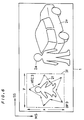
- Fig. 6 illustrates exemplary display on the display unit 204 in a step of making up the total image.
- original image components 2a and 2e are already completely laid out on a total image 1, while processing of an original image component 3f which is a picture is newly in progress.
- the operator properly drives the operation input units 205 while visually recognizing the display image on the display unit 204, to implement the makeup.
- the operator designates a portion (an original image component 2f) of the original image component 3f, which is the object of making up, to be laid out on the total image 1. Namely, he successively indicates start and end points of a plurality of vectors VEC3 forming the contour of the original image component 2f, as shown in Fig. 6.
- the original image component 3f moves to a desired layout position on the total image 1, to designate the layout position.
- the original image components as laid out partially or entirely overlap with each other, he indicates priority in display of the original image components to appear on the display unit for the respective original image components.
- the original image components 2a and 2e for example, the original image component 2a has higher priority.
- he designates shapes of halftone dots, screen rulings and screen angles for the respective original image components. Due to an operation of the CPU 201, various contents of such instructions related to the layout are reflected on the image signals of the corresponding original image components which are stored in the semiconductor memory 202.
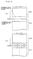
- Fig. 7 is a structural diagram showing structures of a PG signal (at (a)) following an original image component and a CT signal (at (b)) corresponding thereto.
- the PG signal has a header region PGH and a vector signal region PGV.
- An identification signal for identifying a corresponding CT signal is written in the header region PGH when the original image component is a picture, while signals corresponding to the type of a color separation and a density value in tint laying or solid (recording at a halftone dot area rate of 100. %) are written therein when the original image component is not a picture.
- signals expressing a position coordinate value of a base point expressing a layout position, priority of drawing, the shape of the halftone dot, the screen ruling and the screen angle are written in the head region PGH.
- signals expressing start or end point of the vector are written in the vector signal region PGV by relative coordinate values with respect to a base point, while a signal expressing a character or a linework forming the original image component is also written therein when the original image component is the character or the linework.
- the CT signal has a header region CTH and a pixel signal region CTP. Values of widths x and y expressed by pixel numbers along the main scanning direction MS and the subscanning direction SS of the original image component are written in the header region CTH respectively. On the other hand, density values of four types of color separations, i.e., a yellow separation (Y separation), a magenta separation (M separation), a cyan separation (C separation) and a black separation (K separation) are written in the pixel signal region CTP every pixel forming the original image component which is a picture.
- Y separation yellow separation
- M separation magenta separation
- C separation cyan separation
- K separation black separation
- the halftone dot is recorded in units of light spot (spot) of the exposure beam.
- the coordinate values of the aforementioned vectors are in units of ⁇ pixels each formed by integral times the spot such as 2 by 2 spots, for example.
- the aforementioned pixels are formed by integral times the ⁇ pixel, such as 5 by 5 ⁇ pixels.
- Fig. 8 is a process diagram typically showing a flow of this processing. Coordinate values of start and end points of the vectors provided in the PG signal are subjected to the so-called raster conversion, so that positions of ⁇ pixels corresponding to the boundary of the original image component on scanning lines are calculated and converted to the intersection signal.
- Fig. 9 shows an exemplary structure of such an intersection signal.
- the intersection signal is formed by a 32-bit binary signal, for example, and the positions of the aforementioned ⁇ pixels corresponding to the boundary are expressed by addresses on a memory region corresponding to respective spots on the scanning lines.
- a pattern selection signal PPS is adapted to designate one of a plurality of screen patterns as described later, while an attribute signal is adapted to express information such that a tint, a picture or solid is started or ended at the boundary, and a tint value signal is adapted to express density of the tint when the attribute is the tint.
- the so-called "cropping" is carried out on the basis of the CT signal and the positional information on the ⁇ pixels corresponding to the boundary obtained by the raster conversion, to produce image signals corresponding to the total image.
- obtained are an ordinary image signal expressing density of each color separation every pixel in correspondence to an image region which is a picture in the total image, and a high resolution image signal expressing the boundary in units of the ⁇ pixels in correspondence to pixels including the boundary of the original image component.
- the as-obtained three types of signals are stored in the hard disk 203.
- the synthetic unit 300 produces signals expressing density values of the separations in units of the ⁇ pixels on the basis of the intersection, high resolution image and ordinary image signals produced in the work station 200.
- the synthetic unit 300 is formed by hardware with no built-in software, to process the signals at a high speed in synchronization with an operation of the output unit 500 for recording the halftone dots on a photosensitive film or the like. Namely, the synthetic unit 300 processes the signals in units of the respective spots sequentially along the main scanning direction in synchronization with scanning in the output unit 500. Since the output unit 500 comprises four exposure beams to simultaneously record the halftone dots along four scanning lines, the synthetic unit 300 processes the signals simultaneously along a plurality of scanning lines.
- the intersection, high resolution image and ordinary image signals stored in the hard disk 203 are read out and held in a buffer 310 every constant quantity.
- the buffer 310 is adapted to absorb fluctuation in transmission speed from the hard disk 203.
- a synthetic processing unit 320 receives these signals from the buffer 310, and inputs the same in decoders 321 to 323 respectively.
- the decoders 321 to 323 decode these signals, and indicate operations in a superimposing circuit 324 and a switching circuit 325.
- the superimposing circuit 324 outputs the density value of the color separation provided in the ordinary image signal with respect to the pixels when the pixels to be processed are included in those of a picture expressed by the ordinary image signal.
- the superimposing circuit 324 outputs the density value thereof expressed by the high resolution image signal.
- the switching circuit 325 selects either a signal related to a tint or solid provided in the intersection signal or that outputted from the superimposing circuit 324 in correspondence to whether the positions of the ⁇ pixels to be processed are for the tint or the solid, or the picture, and outputs the same as a pixel signal DS expressing density in units of the ⁇ pixels.
- the decoder 321 outputs the pattern selection signal PPS and a separation switching signal PES indicating switching of each color separation in synchronization with successive recording of the halftone dots in the photosensitive film 504 following rotation of the rotary drum 501.
- the pattern selection signal PPS, the separation switching signal PES and the pixel signal DS are temporarily held in the buffer circuit 330, and thereafter inputted in the halftone dot recording apparatus 100 respectively.
- the halftone dot recording apparatus 100 is formed by hardware with no built-in software similarly to the synthetic unit 300, to sequentially process signals in units of spot in synchronization with the operation of the output unit 500 for recording the halftone dots on the photosensitive film 504 or the like.
- the halftone dot recording apparatus 100 first converts the density value of the color separation provided in the pixel signal DS by an SGD (screen gradation) 101 on the basis of a prescribed rule, and reads a screen pattern (SP) signal stored in an SPM (screen pattern memory) 103 by an SPM controller 102.
- the SP signal which forms the basis of formation of the halftone dots, defines a threshold value obtained by making a numerical value in a range of 0 to 255, which can be expressed in an 8-digit binary number, for example, correspond to each one of spots on the aforementioned minimum repeating units of the halftone dots. Therefore, such SP signals generally have different signal volumes in correspondence to the differences between the minimum repeating units of the halftone dots.
- a plurality of, e.g., four types of SP signals are previously prepared in the SPM 103 in response to the respective color separations, so that the SPM controller 102 properly selects one from the same.
- a comparing unit 104 compares the threshold value expressed by the SP signal with the pixel signal DS corrected in the SGD 101 every spot, to output a halftone dot signal in response to the result of the comparison.
- Fig. 1 is a circuit diagram showing an internal circuit of the halftone dot recording apparatus 100.
- the exemplary apparatus shown in the circuit diagram of Fig. 1 is so formed as to sequentially process spots on four scanning lines in parallel with each other on the premise that the output unit 500 is provided with four exposure beams.
- Clock pulse signals IRCK, DPLS, SELCK and CMPCK are generated from a timing control circuit (not shown), to repeatedly rise in synchronization with operations of the output unit 500 for recording the halftone dots for the respective spots.
- Latches DL1 to DL3 and DL4a to DL4d sequentially hold the separation switching signal PES, the pattern selection signal PPS and pixel signals DSa to DSd outputted from the buffer circuit 330 in synchronization with these clock pulses.
- the SPM 103 is provided with for SPMs 103a to 103d in parallel with each other, in correspondence to the four exposure beams.
- Each of the SPMs 103a to 103d is a random access memory (RAM), which previously stores four types of SP signals at the maximum every color separation, i.e., 16 types of SP signals at the maximum in total, in advance of starting of image recording processing.
- Address signal lines and data signal lines which are connected to the SPM 103 are switched by a tristate buffer (not shown) or the like, for example, to form parts of the memory region of the CPU 201, thereby writing the SP signals. Since single scanning is carried out by four exposure beams according to this embodiment, the respective SPMs 103a to 103d store SP signals of scanning lines exposed by the corresponding exposure beams.
- Each of data selectors SELa to SELd is a circuit having a function of selecting one from four types of 15-bit input signals on the basis of the pattern selection signal PPS and outputting the same.
- Address generation controllers AGCp to AGCs output address signals AS2p to AS2s designating storage positions of the SP signals respectively when the SP signals stored in the SPMs 103a to 103d are read out.
- Such four address generation controllers AGCp to AGCs are provided to output four address signals AS2p to AS2s, since one is selected from four types of halftone dots with respect to one separation.
- Fig. 10 is a block diagram showing an internal structure of the address generation controller AGCp.
- the remaining address generation controllers AGCq to AGCs also have similar structures.
- An address control table memory 111p previously stores address control signals following storage of the SP signals in the SPM 103.
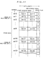
- Fig. 11 shows structures of the address control signals.
- the address control signals have start address signals, end address signals and ending flags. Referring to Fig. 11, an address control signal in a storage position designated by addresses ad0 to ad9 corresponds to a SP signal of a first separation, and an address control signal in addresses ad16 to ad21 corresponds to an SP signal of a second separation, for example.
- the address control table memory 111p stores address control signals corresponding to four types of SP signals which are employed for the four types of color separations.
- the ending flags which are signals having 1-bit data lengths, have values "1" in final addresses of the respective SP signals and values "0" in other addresses.
- first and second SP signals are formed by 40 (10 x 4) and 24 (6 x 4) spots respectively. These numbers correspond to sizes of the minimum repeating units of the halftone dots formed by the respective SP signals (minimum repeating units of the SP signals) along the subscanning direction, i.e., numbers of spots of the SP signals defining threshold values arranged along the subscanning direction.
- the sizes of the minimum repeating units of the SP signals along the main scanning direction i.e., the numbers of the spots of the SP signals defining the threshold values arranged along the main scanning direction are provided by differences between the respective end address signals and the start address signals.
- address and data signal lines which are connected to the address control table memory 111p are switched to form parts of the memory regions of the CPU 201, so that the address control signals are written in the address control table memory 111p, similarly to the aforementioned SP signals.
- the address control signals for the corresponding color separation are stored in four regions divided by high-order two bits of the addresses respectively.
- the 2-bit separation switching signal PES is inputted in a halftone dot code generation control circuit 112p.
- This halftone dot code generation control circuit 112p latches the received separation switching signal PES as a separation designating signal, and transmits the as-latched separation switching signal PES and control signals described later to a subaddress counter 113p and the address control table memory 111p.
- the subaddress counter 113p comprises four types of counters in correspondence to the respective color separations.
- a count signal is inputted in the address control table memory 111p from a counter corresponding to the separation designated by the halftone dot code generation control circuit 112p.
- the address control table memory 111p supplies a start address signal in an address obtained by adding a count value expressed by the count signal outputted from the subaddress counter 113p to an address (high order 2 bits) designated by the halftone dot code generation control circuit 112p to a main address counter 115p, and supplies an end address signal to a first coincidence detection circuit 116p.
- the main address counter 115p holds the start address signal, and outputs the same to the data selectors SELa to SELd as the address signal AS2p.
- the main address counter 115p further successively increments the value of the held signal in synchronization with the clock pulse DPLS, to output the same as the address signal AS2p.
- this address signal AS2p is supplied to the SPM. 103 through the data selectors SELa to SELd, SP signals along first to fourth scanning lines, for example, are successively read from the SPM 103.
- the output of the main address counter 115p is also supplied to the first coincidence detection circuit 116p, so that a first coincidence signal is outputted from the first coincidence detection circuit 116p to the main address counter 115p when the output coincides with the end address signal.
- the main address counter 115p restores its output to a start address signal again when the same receives the first coincidence signal, to repeat a similar operation.
- a series of SP signals along the first to fourth scanning lines are repeatedly read from the SPM 103. In other words, the minimum repeating units of the SP signals along the main scanning direction are repeatedly read out.
- the separation switching signal PES from the decoder 321 changes and the halftone dot code generation control circuit 112p latches this signal to transmit the same to the address control table memory 111p and the subaddress counter 113p.
- the address control table memory 111p outputs start and end address signals for a new separation, to supply the same to the main address counter 115p and the first coincidence detection circuit 116p respectively. Consequently, the main address counter 115p holds the start address signal for the new separation, and outputs an address signal AS2p for the new separation.
- a main scanning spot number register 118p previously stores a spot number corresponding to a recording range along the main scanning direction.
- a spot number counter 119p counts the clock pulse DPLS.
- a second coincidence detection circuit 120p compares this count value with the spot number stored in the main scanning spot number register 118p, to output a second coincidence signal to the halftone dot code generation control circuit 112p and the subaddress counter control circuit 114p when the values coincide with each other.
- the second coincidence signal indicates ending of recording operations on scanning lines (first to fourth scanning lines, for example).
- control signals indicating 0 to 3 are transmitted regardless of the separation switching signal PES, which is an input signal, in a short time before starting of next scanning lines (fifth to eighth scanning lines, for example), to successively select the counters for the respective separations provided in the subaddress counter 113p.
- address control signals stored in current addresses corresponding to the respective separations are successively outputted from the address control table memory 111p, so that ending flags therein are inputted in the subaddress counter control circuit 114p.
- the subaddress counter control circuit 114p outputs a count clock pulse or a reset pulse to the subaddress counter 113p every corresponding separation in response to the value of "0" or "1" of the ending flag when the second coincidence signal is inputted. If an ending flag corresponding to the Y separation is "0", for example, the subaddress counter control circuit 114p outputs one count clock pulse corresponding to the Y separation when the second coincidence signal is inputted. Thus, the counter of the subaddress counter 113p corresponding to the Y separation increments its count signal by 1. When the ending flag corresponding to the Y separation is "1", on the other hand, the subaddress counter control circuit 114p outputs one reset pulse corresponding to the Y separation. Thus, the counter of the subaddress counter 113p corresponding to the Y separation restores its count signal to zero. This also applies to the remaining separations.
- the address control table memory 111p supplies a start address signal in an address which is obtained by adding a count value expressed by a new count signal outputted from the subaddress counter 113p to the address designated by the halftone dot code generation control circuit 112p in response to the separation switching signal PES to the main address counter 115p, and supplies an end address signal to the first coincidence detection circuit 116p.
- reading of the SP signals from the SPM 103 is updated in the subscanning direction, and returned to the initial stage upon completion of the minimum repeating units in the subscanning direction, to repeat a similar operation. Namely, the minimum repeating units of the SP signals in the subscanning direction are repeatedly read out from the SPM 103.
- the minimum repeating units of the SP signals are two-dimensionally repeatedly read from the SPM 103 along both of the main scanning and subscanning directions.
- one of the SP signals is properly selected from plural types of SP signals previously stored in the respective SPMs 103a to 103d in response to the separation switching signal PES every color separation, and further properly selected in response to the pattern selection signal PPS every original image component. Since the minimum repeating units of these SP signals are generally different from each other, one of the address signals is properly selected from the address signals AS2p to AS2s generated by the address generation controllers AGCp to AGCs by the data selectors SELa to SELd, to be inputted in the SPMs 103a to 103d respectively.
- the SGD 101 is provided with four parallel SGDs 101a to 101d in correspondence to the four exposure beams.
- the SGDs 101a to 101d convert density values of a certain color separation provided in the pixel signals DSa to DSd outputted from the latches DL4a to DL4d in response to the separation switching signal PES and the pattern selection signal PPS on the basis of generally different conversion tables every color separation and original image component, to output the converted values as correction density signals MDSa to MDSd respectively.
- address and data signal lines which are connected to the SGD 101 are switched to form parts of the memory region of the CPU 201 so that the correction density signals are written similarly to the aforementioned SP signals.
- the comparing unit 104 is provided with four parallel comparators 104a to 104d in correspondence to the four exposure beams. These comparators 104a to 104d compare the correction density signals MDSa to MDSd received from the SGDs 101a to 101d with the SP signals received from the SPMs 103a to 103d respectively.
- the comparator 104a outputs a value "1" as a halftone dot signal DOTa when the correction density signal MDSa is greater than the SP signal, and outputs a value "0" in other case.
- the comparators 104b to 104d also output halftone dot signals DOTb to DOTd.
- the four exposure beams provided in the output unit 500 record halftone dots in response to these halftone dot signals DOTa to DOTd respectively.
- the output unit 500 emits four exposure beams, and each part of the halftone dot recording apparatus 100 responsively comprises four systems in parallel with each other.
- the output unit 500 may emit a single exposure beam, and the halftone dot recording apparatus 100 is implemented in a circuit shown in Fig. 12 in this case.
- each of an SGD 101, an SPM controller 102, an SPM 103 and a comparing unit 104 has only one system corresponding to one scanning line.
- an address generation controller which corresponds to types of SP signals, is provided with four systems even if one scanning line is to be simultaneously scanned.
- Other structure shown in Fig. 12 is identical to that of the embodiment shown in Fig. 1, and hence elements corresponding to those appearing in Fig. 1 are denoted by the same reference numerals, to omit redundant description.
- the address signals AS2p to AS2s outputted from the plurality of address generation controllers AGCp to AGCs are supplied to the data selectors SELa to SELd respectively. Then, only one address signal is supplied to the SPMs 103a to 103d on the basis of the pattern selection signal PPS, to output only a corresponding SP signal.
- a structure for outputting an SP signal corresponding to a pattern selection signal PPS is not restricted to this.
- the SPM 103a is formed by four memories, so that respective types of SP signals are stored in the respective memories. Only corresponding ones of the address signals AS2p to AS2s are supplied to these memories, and SP signals are outputted from the respective memories in a parallel manner. Then, only an SP signal corresponding to the pattern selection signal PPS is selected by a data selector. This also applies to the SPMs 103b to 103d.
- the SPM 103 stores SP signals which are based on rational tangents in the aforementioned embodiment, the same may alternatively store SP signals which are based on irrational tangents.
Applications Claiming Priority (2)
| Application Number | Priority Date | Filing Date | Title |
|---|---|---|---|
| JP267978/92 | 1992-09-09 | ||
| JP4267978A JP2763992B2 (ja) | 1992-09-09 | 1992-09-09 | 網点記録装置 |
Publications (1)
| Publication Number | Publication Date |
|---|---|
| EP0587152A1 true EP0587152A1 (en) | 1994-03-16 |
Family
ID=17452219
Family Applications (1)
| Application Number | Title | Priority Date | Filing Date |
|---|---|---|---|
| EP93114449A Withdrawn EP0587152A1 (en) | 1992-09-09 | 1993-09-08 | Halftone dot recording method and apparatus |
Country Status (3)
| Country | Link |
|---|---|
| US (1) | US5530555A (ja) |
| EP (1) | EP0587152A1 (ja) |
| JP (1) | JP2763992B2 (ja) |
Cited By (1)
| Publication number | Priority date | Publication date | Assignee | Title |
|---|---|---|---|---|
| WO1995027365A1 (en) * | 1994-03-30 | 1995-10-12 | Hersch, Roger, D. | Method and apparatus for generating halftone images by evolutionary screen dot contours |
Families Citing this family (2)
| Publication number | Priority date | Publication date | Assignee | Title |
|---|---|---|---|---|
| US5754746A (en) * | 1995-12-18 | 1998-05-19 | Xerox Corporation | Multi bit per pixel compression/decompression using parallel encoded streams |
| JP3574036B2 (ja) * | 1999-08-24 | 2004-10-06 | シャープ株式会社 | インクジェット画像形成方法 |
Citations (6)
| Publication number | Priority date | Publication date | Assignee | Title |
|---|---|---|---|---|
| FR2397112A1 (fr) * | 1977-07-07 | 1979-02-02 | Xerox Corp | Procede et appareil de tramage de similigravure electronique |
| FR2516329A1 (fr) * | 1981-11-07 | 1983-05-13 | Dainippon Screen Mfg | Procede d'enregistrement electronique d'images en demi-teintes |
| EP0293214A2 (en) * | 1987-05-29 | 1988-11-30 | Digital Equipment Corporation | System for producing dithered images on asymmetric grids |
| WO1991016783A1 (de) * | 1990-04-26 | 1991-10-31 | Linotype-Hell Ag | Verfahren zur digitalisierten rasterung einer halbton-bildvorlage |
| EP0464650A2 (en) * | 1990-06-28 | 1992-01-08 | Dainippon Screen Mfg. Co., Ltd. | Method of and apparatus for producing halftone dot image |
| EP0493935A2 (en) * | 1990-12-31 | 1992-07-08 | E.I. Du Pont De Nemours And Company | Digital electronic system for halftone printing |
Family Cites Families (8)
| Publication number | Priority date | Publication date | Assignee | Title |
|---|---|---|---|---|
| US3742129A (en) * | 1971-07-07 | 1973-06-26 | Harris Intertype Corp | Apparatus and method for generating halftones for image reproduction |
| US4149183A (en) * | 1976-05-21 | 1979-04-10 | Xerox Corporation | Electronic halftone generator |
| JPS61285867A (ja) * | 1985-06-12 | 1986-12-16 | Dainippon Screen Mfg Co Ltd | 網点画像記録方法並びに装置 |
| US4903123A (en) * | 1987-06-10 | 1990-02-20 | Canon Kabushiki Kaisha | Image processing apparatus using inclined line screens to reduce Moire |
| JPH0279670A (ja) * | 1988-09-16 | 1990-03-20 | Dainippon Screen Mfg Co Ltd | 網目版画像走査記録装置 |
| US4924301A (en) * | 1988-11-08 | 1990-05-08 | Seecolor Corporation | Apparatus and methods for digital halftoning |
| US4918622A (en) * | 1988-11-16 | 1990-04-17 | Eastman Kodak Company | Electronic graphic arts screener |
| DE9116783U1 (de) * | 1991-04-22 | 1993-12-09 | Habermeyer Willy | Überwachungssystem für eine Tankstelle |
-
1992
- 1992-09-09 JP JP4267978A patent/JP2763992B2/ja not_active Expired - Fee Related
-
1993
- 1993-08-11 US US08/104,706 patent/US5530555A/en not_active Expired - Fee Related
- 1993-09-08 EP EP93114449A patent/EP0587152A1/en not_active Withdrawn
Patent Citations (6)
| Publication number | Priority date | Publication date | Assignee | Title |
|---|---|---|---|---|
| FR2397112A1 (fr) * | 1977-07-07 | 1979-02-02 | Xerox Corp | Procede et appareil de tramage de similigravure electronique |
| FR2516329A1 (fr) * | 1981-11-07 | 1983-05-13 | Dainippon Screen Mfg | Procede d'enregistrement electronique d'images en demi-teintes |
| EP0293214A2 (en) * | 1987-05-29 | 1988-11-30 | Digital Equipment Corporation | System for producing dithered images on asymmetric grids |
| WO1991016783A1 (de) * | 1990-04-26 | 1991-10-31 | Linotype-Hell Ag | Verfahren zur digitalisierten rasterung einer halbton-bildvorlage |
| EP0464650A2 (en) * | 1990-06-28 | 1992-01-08 | Dainippon Screen Mfg. Co., Ltd. | Method of and apparatus for producing halftone dot image |
| EP0493935A2 (en) * | 1990-12-31 | 1992-07-08 | E.I. Du Pont De Nemours And Company | Digital electronic system for halftone printing |
Cited By (1)
| Publication number | Priority date | Publication date | Assignee | Title |
|---|---|---|---|---|
| WO1995027365A1 (en) * | 1994-03-30 | 1995-10-12 | Hersch, Roger, D. | Method and apparatus for generating halftone images by evolutionary screen dot contours |
Also Published As
| Publication number | Publication date |
|---|---|
| JPH0698154A (ja) | 1994-04-08 |
| US5530555A (en) | 1996-06-25 |
| JP2763992B2 (ja) | 1998-06-11 |
Similar Documents
| Publication | Publication Date | Title |
|---|---|---|
| US4700235A (en) | Method and apparatus for producing half-tone printing forms with rotated screens on the basis of randomly selected screen threshold values | |
| US4775886A (en) | Apparatus for performing a plurality of editing processes according to a predetermined order of priority while recording a composite image | |
| US4577219A (en) | Method and an apparatus for copying retouch in electronic color picture reproduction | |
| SU1494857A3 (ru) | Способ частично выравнивающей ретуши при репродукции цветовых изображений | |
| US4825298A (en) | Halftone dot-generator and generating method | |
| JPH10334228A (ja) | ラスタ画像の解像度向上方法 | |
| EP0493935B1 (en) | Digital electronic system for halftone printing | |
| US5585945A (en) | Image synthesis with reduced memory requirements | |
| US6853467B2 (en) | Multistage screening with screens of any desired screen resolutions and screen angles | |
| US5850295A (en) | Image recording apparatus | |
| US5294996A (en) | Image processing apparatus adaptable for use at variable resolution | |
| US4930023A (en) | Halftone dot generator using grained screen patterns | |
| EP0369302B1 (en) | Method of and apparatus for producing halftone image | |
| US6678426B1 (en) | Programmable mapping of lower resolution digital data to a higher resolution for output on a lower resolution device | |
| EP0457511A2 (en) | Apparatus for generating a screened reproduction of an image | |
| EP0359266B1 (en) | Method of and apparatus for recording halftone image | |
| US5530555A (en) | Method and apparatus for recording halftone dot image with different repeating units | |
| JPS60121878A (ja) | 画像走査複製方法 | |
| JPH0519862B2 (ja) | ||
| EP0488118B1 (en) | Image recording apparatus for high quality images | |
| US5268772A (en) | Method of and apparatus for obtaining halftone image | |
| JP3384115B2 (ja) | 画像処理装置 | |
| EP0319976A2 (en) | Method of and apparatus for recording image in the form of pixel array | |
| GB2196508A (en) | Method of forming halftone dots | |
| US5608822A (en) | Apparatus and method for generating half-tone dot in image reproduction |
Legal Events
| Date | Code | Title | Description |
|---|---|---|---|
| PUAI | Public reference made under article 153(3) epc to a published international application that has entered the european phase |
Free format text: ORIGINAL CODE: 0009012 |
|
| AK | Designated contracting states |
Kind code of ref document: A1 Designated state(s): DE FR GB |
|
| 17P | Request for examination filed |
Effective date: 19940616 |
|
| 17Q | First examination report despatched |
Effective date: 19981105 |
|
| STAA | Information on the status of an ep patent application or granted ep patent |
Free format text: STATUS: THE APPLICATION IS DEEMED TO BE WITHDRAWN |
|
| 18D | Application deemed to be withdrawn |
Effective date: 19990316 |