EP0585881A2 - Imprimante en série - Google Patents
Imprimante en série Download PDFInfo
- Publication number
- EP0585881A2 EP0585881A2 EP93113914A EP93113914A EP0585881A2 EP 0585881 A2 EP0585881 A2 EP 0585881A2 EP 93113914 A EP93113914 A EP 93113914A EP 93113914 A EP93113914 A EP 93113914A EP 0585881 A2 EP0585881 A2 EP 0585881A2
- Authority
- EP
- European Patent Office
- Prior art keywords
- carriage
- signal
- reference voltage
- output
- generating
- Prior art date
- Legal status (The legal status is an assumption and is not a legal conclusion. Google has not performed a legal analysis and makes no representation as to the accuracy of the status listed.)
- Granted
Links
Images


Classifications
-
- B—PERFORMING OPERATIONS; TRANSPORTING
- B41—PRINTING; LINING MACHINES; TYPEWRITERS; STAMPS
- B41J—TYPEWRITERS; SELECTIVE PRINTING MECHANISMS, i.e. MECHANISMS PRINTING OTHERWISE THAN FROM A FORME; CORRECTION OF TYPOGRAPHICAL ERRORS
- B41J19/00—Character- or line-spacing mechanisms
- B41J19/18—Character-spacing or back-spacing mechanisms; Carriage return or release devices therefor
- B41J19/20—Positive-feed character-spacing mechanisms
- B41J19/202—Drive control means for carriage movement
- B41J19/205—Position or speed detectors therefor
- B41J19/207—Encoding along a bar
Definitions
- the present invention relates generally to a serial printer and, more particularly, to a serial printer including a synchronous signal generating circuit for synchronizing a movement of a carriage mounted with a printing head with a recording action of the recording head.
- a serial printer performs a record (print) while causing a carriage mounted with a printing head of a recording means to scan across a recording medium. If a carriage speed fluctuates due to some influence, however, a scatter in density appears as a result of recording. Especially in a color printer, the problem is a deviation in terms of color registration.
- One of known methods of obviating these problems has hitherto involved steps of detecting a moving quantity of the carriage mounted with the recording means with respect to an apparatus body and performing a recording action through the recording means while synchronizing with this detected result.
- a scale portion of a linear encoder is fixed to the apparatus body.
- the carriage which moves relatively to this scale portion is mounted on a detecting portion of the linear encoder.
- an output signal from this detecting portion is amplified and thereafter fetched outside the carriage.
- a recording signal is generated in synchronization with this amplified signal, thereby preventing occurrences of the scatter in the printing density and of the deviation in the color registration.
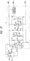
- Fig. 44 is a circuit diagram showing a configuration of a synchronous signal generating circuit in the conventional example.
- the scale portion of the linear encoder is mounted in the carriage and fixed to the apparatus body.
- a detecting portion 101 of the linear encoder detects a relative moving position of the carriage with respect to the apparatus body by detecting the scale portion.
- the detecting portion 101 consisting of MR elements which act based on a magnetic resistance effect is provided integrally with a pair of magnetic detecting elements 102, 103.
- This detecting portion 101 is also connected to a substrate 5 mounted on the carriage and shown by a broken line in the Figure.
- amplifiers 104, 105 constituting constant current circuits, an amplifier 106 for amplifying a detected signal and a comparator 107.
- An output signal 303 is thereby outputted.
- a variable resistor 158 for determining a reference voltage is connected to the comparator 107 and packaged on the substrate 5. An adjustment thereof is thus made on the carriage.
- the magnetic detecting elements 102, 103 are supplied with a constant current via the constant current circuits 104, 105, respectively. Magnetic patterns are previously recorded at a fixed interval on the scale portion of the linear encoder which is fixed to the apparatus body.
- the detecting portion 101 moves along the scale portion. With this movement, resistance values of the magnetic detecting elements 102, 103 vary. The variation in the resistance value is detected as a change in voltage and amplified by the amplifier 106.
- An amplified signal is inputted to one input terminal of the comparator 107.
- This comparator 107 compares the amplified signal with a reference voltage preset by an adjustment of the variable resistor 158 and inputted to the other input terminal of the comparator 107.
- An output signal 303 is thereby obtained as a synchronous signal.
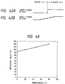
- Fig. 45A is a diagram showing a relationship of the reference voltage versus the signal inputted to the comparator 107.
- Fig. 45B is a pulse waveform diagram showing a relationship of the output signal 303 of the comparator 107 in combination with Fig. 45A.
- An input signal 301 to the comparator 107 takes, as depicted in the Figure, a waveform approximate to a sine waveform which varies with a fixed period.
- the pulse-shaped output signal 303 of the comparator in consequence of obtaining the reference voltage as a threshold value, a difference between the input signal 301 and the reference voltage 302 appears, as can be understood from the Figure, in the form of a duty change in the output signal. If the recording/printing action is executed in synchronization with this output signal 303, the scatter in the density and a ruled-line deviation in an output image are caused. This results in a remarkable decline in terms of recording quality.
- Figs. 46A and 46B are explanatory views of the recording action, showing how dots D are recorded on a recording medium by driving a recording means in synchronisation with the output signal 303 described above.
- a fluctuation in pitch P between the dots D can be seen, and consequently, the scatter in the density is produced as a result of recording. Particularly in the color printer, this may cause the deviation in the color registration.
- the recording/printing action is effected synchronizing with the output signal. Therefore, the duty change in the output signal pulse waveform leads directly to the decline in quality as a result of printing.
- a means for restraining the duty change in the output signal pulse waveform depends on a stability of the circuit elements themselves. Hence, expensive parts have to be employed. A problem arises in terms of increasing the costs.
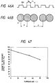
- Fig. 47 is a graphic chart showing a temperature dependency characteristic with respect to a magnetic resistance effect rate of the MR element.
- Fig. 48 is a graphic chart showing a temperature dependency characteristic with respect to a resistance value of the MR element.
- the MR element expressed by the preceding formula and shown in Figs. 47, 48 has the large temperature dependency characteristic, and hence, its output becomes as illustrated in Fig. 17.
- Fig. 49A is a waveform diagram showing a relationship of the reference voltage 302 versus the signal 301 inputted to the comparator 107.
- Fig. 49B is a waveform diagram of the synchronization output signal 303 obtained when establishing the relationship shown in Fig. 49A.
- the input signal 301 to the comparator 107 assumes a waveform approximate to the sine waveform which varies, as shown in the Figure, with a fixed period.
- Fig. 1 is a perspective view illustrating the principal portion of a serial printer together with a recording medium.
- a carriage 1 indicated by a one-dotted line is mounted with a recording portion 1h based on an inject recording method.
- the carriage 1 is guided by a guide shaft member 11 formed with a helical groove in the outer peripheral surface thereof.
- An engagement portion (unillustrated) is propelled along the helical groove with rotations of the guide shaft member 11.
- the carriage 1 is thus reciprocated in arrowed directions in the Figure with respect to a recording sheet 13 wounded on the outer peripheral surface of a platen 12. Dots D are recorded at pitches P on the recording sheet (recording medium) 13, thus forming an image or a character.
- a so-called serial printer is constructed in this manner.
- the thus constructed carriage 1 incorporates an encoder for obtaining a synchronous signal.
- This encoder is a magnetic linear encoder.
- the following is an arrangement thereof.
- a magnetic pattern is recorded with a printing pitch density corresponding to, e.g., 180 dot/inch (dpi) or 360 dpi on a magnetic substance formed on a wire surface.
- a scale portion 501 of the linear encoder is fixed to an apparatus body 100.
- a magnetic head 502 composed of MR elements, etc. is fixed inwardly of the carriage 1. A positional detection is thereby attainable with the movements of the carriage 1.
- a flexible printed circuit board 503 for fetching output signals to the outside from the MR elements in the magnetic head is connected to the magnetic head 502.
- a connecting portion 504 is connected to a connector (not shown), thus making a connection to a substrate 5 mounted on the carriage 1 and shown by a broken line in the Figure.
- FIG. 2 is a basic block diagram in a first embodiment of the present invention.
- a duty change restraining means according to this invention designated at 215 in the Figure, is constructed of a duty observing means 215a, a detecting means 215b and a control means 215c.
- a control output from the duty change restraining means 215c is transferred to a control input of a reference voltage 302 of a DC voltage source 211.
- the reference voltage 302 serves as an output generation threshold with respect to an input signal 301 inputted to a comparator 107 via an amplifying portion 106 from a detecting portion 101.
- the reference voltage 302 is thereby stabilized with respect to a duty of the output signal.
- Figs. 3 and 4 illustrate examples of circuitry based on the block diagram (Fig. 2).
- the detecting portion 101 is provided with magnetic detecting elements (MR elements) 102, 103.
- a magnetic part of the scale portion of the linear encoder is scanned by the magnetic detecting elements 102, 103.
- Variations in magnetic resistance in the magnetic detecting elements are thereby detected based on the circuitry of the substrate 5.
- Constant current sources 104, 105 in the circuit of the substrate 5 give a proper bias to a lever as a whole in order to detect negative signals through the MR elements.
- a result of scanning magnetic characteristics of the scale portion of the linear encoder by the detecting portion 101 is approximate to a sine wave and the transmitted to the amplifying portion 106.
- This sine wave is converted into a pulse output with the reference voltage 302 serving as a threshold value.
- the comparator 107 is provided therefor and outputs an output signal 303.
- a pulse duty of this output signal 303 is compared and examined.
- a duty change restraining means (which will be mentioned later) constructed in a control circuit substrate 4 generates an input data signal 150 so that a duty ratio becomes 50%.
- the input data signal 150 is transferred to a D/A (digital-to-analog) converter 149.
- the D/A converter 149 converts the input data signal defined as a digital value into a control voltage signal 151 as an analog value.
- the control voltage signal 151 is inputted to a DC voltage source consisting of transistors Q111, Q112.
- the DC voltage source 211 generates the reference voltage 302 having a proper voltage value on the basis of the control voltage signal 151.
- the reference voltage 302 is inputted to one input terminal of the comparator 107.
- Fig. 4 is a circuit block diagram of the above-mentioned duty change restraining means. Indicated at 705 in Fig. 4 is a differentiating circuit, to which the output signal 303 is inputted from the comparator, for detecting a switchover of the level of the output signal 303.
- An MPU 701 controls actions of the respective functional elements.
- a counter 702 measures an output pulse width (in other terms, a duty).
- a buffer 703 temporarily stores a count value of the counter 702.
- a memory 704 stores a control algorithm and a table of the threshold values.
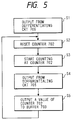
- Fig. 5 is a flowchart showing actions of the observing means in the duty change restraining means.
- the differentiating circuit 705 gives forth a trigger output to the MPU 701 (step S1).
- the MPU 701 receiving the trigger output causes, after resetting the counter 702 (step S2), the counter 702 to start counting for measuring a pulse width of the output signal (step S3).
- the level of the output signal 303 is inverted.
- the differentiating circuit 705, when the level is inverted gives forth a trigger output (step S4).
- the MPU 701 outputs the count value of the counter 702 to the buffer 703 (step S5).
- the MPU recognizes that the data of the count value has been inputted to the buffer 703.
- the action goes back to step S2.
- the same steps as those described above are hereinafter sequentially repeated, thus observing the duty of the output pulse.
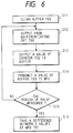
- Fig. 6 is a flowchart showing actions of the detecting means in the duty change restraining means.
- contents of the buffer 703 are cleared when setting the system (step S11).
- a trigger is outputted from the differentiating circuit 705 at a rise (or a fall) of the output signal 303 with a printing action (step S12).
- the MPU 701 detects the trigger, and the count value of the counter 702 is transferred to the buffer 703 (step S13).
- the MPU 701 detects that a value of the buffer 703 is updated.
- the duty is detected in the MPU 701. For this purpose, the data thereof are taken in from the buffer 703 (step S14).
- the MPU 701 after finishing a measurement of the pulses for one period, judges whether or not two values, i.e., a width at a High level (Th in Figs. 8A and 8B) and a width at a Low level (Tl in Figs. 8A and 8B), have been detected, these two values serving for calculating the duty (step S15). If not, the action returns to step S12. Whereas if detected, the action proceeds to next step S16. Then, just when obtaining the two values to be compared, a difference between two values is taken at MPU 701, and the widths are compared (step S16).
- Fig. 7 is a flowchart showing actions of the control means in the duty change restraining means.
- the MPU 701 accesses the memory 704 with respect to a compared value obtained through the detecting means as well as through the observing means described above (step S21).
- the MPU 701 then refers to the threshold value (step S22).
- the widths Th, Tl of the signal 303 in Figs. 8A and 8B are taken in as items of count value data by the MPU 701.
- the MPU 701 compares magnitudes of the widths. If there is a change in the duty ratio, and when Th > Tl, it is required that the reference voltage 302 be decreased. When Th ⁇ Tl, it is required that the reference voltage be increased.
- Judged is whether or not a Th-to-Tl relationship in magnitude needs a modification of the data 150 in comparison with the threshold value determined by the system (step S23).
- an optimum reference voltage control table is drawn out of the memory 704 (step S24).
- the correction value data is outputted to the D/A converter 149 (step S26).
- a present value of the correction value data 150 is kept (step S25).
- the output signal 303 is controlled so that the pulse widths Th, Tl are substantially uniformly kept (i.e., the duty ratio is 50%) as seen in a pulse 157 exhibiting an output voltage waveform in Fig. 8A.
- the pitches P of the printing outputs (dots) D become uniform.
- the observation of the pulse duty ratio of the output signal 303 involves the use of the counter and the system clocks, wherein the "H (High)” and “L (Low)" times of the output pulse are measured.
- a compared value between the High- and Low-level widths is grasped as an electric power ratio in terms of restraining a duty change while keeping the duty ratio at 50% by a method other than the above-mentioned.
- a duty observing portion is composed of discrete parts.
- Fig. 9 is a circuit block diagram of the duty change restraining means in the second embodiment.
- a power integrator generally designated at 801 in Fig. 9 accumulates the electric power proportional to lengths of the pulse width Th, Tl of the output signal 303.
- Low-pass filters 802a, 802b fetch charge electric power as a DC component from the power integrator 801.
- Voltage control oscillators 803a, 803b each change an oscillation frequency with respect to the output voltages from the low-pass filters 802a, 802b.
- a phase comparator 805 compares phases of the output frequencies of the voltage control oscillators 803a, 803b and outputs a phase jitter in the form of a variation in voltage.
- a duty change of the output signal 303 is outputted as a fluctuation in voltage of a phase comparator 805. Namely, the pulse widths "Th", “Tl” of the output signal 303 are observed by the power integrator.
- the duty change is, when recognized, detected as a variation in the output voltage. This is detected as a voltage variation and therefore matched with a next-stage control signal voltage via a transfer filter 804.
- the reference voltage 302 is controlled by a voltage control constant voltage source 806, with this voltage serving as a control signal of the voltage control constant voltage source 806.
- Fig. 10 is a diagram of the circuit ranging from the power integrator 801 to the phase comparator 805 in the duty change restraining means of Fig. 9. A configuration and actions of this circuit will hereinafter be explained.
- a construction consisting of transistors Q1 - Q3 and capacitors C1, C2
- electric charges are accumulated in the capacitor C1 for a High-time (i.e., a Th-time) of the output pulse 303.
- the electric charges are accumulated in the capacitor C2 for a Low-time (i.e., a Tl-time) of the output pulse 303.
- the electric charges accumulated in the capacitors C1, C2 pass through low-pass filters LPF 802a, 802b composed of a capacitor C11 and resistors R12, R13 and of a capacitor C12 and resistors R11, R14.
- the electric charges are transferred as DC potentials to VCOs (voltage control oscillators) 803a, 803b.
- the VCO 803a is constructed of a constant current source consisting of transistors Q22, Q23, Q27, Q28 and a Schmidt trigger circuit consisting of transistors Q41, Q42, Q43, Q44.
- the VCO 803b is also constructed of a constant current source consisting of transistors Q20, Q21, Q24, Q25 and a Schmidt trigger circuit consisting of transistors Q31, Q32, Q33, Q34.
- Two outputs from these VCOs are inputted to the phase comparator 805 composed of transistors Q51 - Q58.
- An output from this phase comparator 805 is transferred via an LPF consisting of R61, R62, C61 to the transfer filter 804 (see Fig. 9, but not shown in Fig. 10). This output is transferred next to the voltage control constant voltage source 806 (see Fig. 9, but not shown in Fig. 10).
- Fig. 11 illustrates waveforms when a duty change observing means circuit of the duty change restraining means is open on the occasion of opening a transfer block of the duty change restraining means.
- the reference voltage 302 assuming a pulse generation threshold level changes with respect to a waveform of the input signal 301
- the High- and Low-level widths "Th", "Tl" of the wave form of the output signal 303 change.
- This pulse width information is converted into electric potentials Vd1, Vd2 by means of the power integrator 801 and the LPFs 802a, 802b.
- the electric potentials are respectively inputted to the VCOs 803a, 803b.
- Vd1 corresponds to Tl
- Vd2 corresponds to Th.
- the voltage source 806 is controlled by closing the control loop so that the output of the phase comparator 805 is always ⁇ 0.
- the waveform of the output signal 303 can thereby hold the duty ratio 50%.
- the voltage source 806 is exactly controlled by the phase comparator 805.
- a transfer function of the transfer filter 804 an arbitrary function in a linear or non-linear form is given corresponding to an output characteristic of the phase comparator 805.
- the frequency of the output signal pulse 303 fluctuates at stages of the acceleration and deceleration. If the pulse duty ratio of "Th", "Tl” does not change, however, a difference output is taken out at the next stage of the power integrator 801 and inputted to VCO. Consequently, no influence is exerted on the output of the phase comparator 805.
- the electric power is integrated in accordance with the output signal pulse widths "Th", "Tl".
- the duty change is observed by use of the phase comparator and the VCOs. As illustrated in Fig. 12, however, the output voltages of the power integrator 801 are compared by a subtracter (voltage comparator) 901. The duty ratio 50% of the output pulse 303 can be obtained even by controlling the reference voltage 302 so that a difference therebetween is zeroed.
- Fig. 13 is a circuit diagram in a fourth embodiment.
- the detecting portion 101 is, as in the same way with the first to third embodiments, incorporated into the magnetic head 502.
- the detecting portion 101 is constructed of the magnetic detecting elements 102, 103 which act based on the MR (magnetic resistance) effect.
- the magnetic detecting elements 102, 103 are also similarly connected to amplifiers 104, 105 which constitute a constant current circuit.
- the amplifiers 104, 105 are further connected to an amplifier 106 for amplifying a detected signal and a comparator 107.
- an interior of the detecting portion 101 is provided with a temperature measuring portion 160 consisting of an element the resistance value of which varies depending on a temperature as in the case of a thermistor.
- a variation in the temperature is detected as a fluctuation in voltage when a constant current flows therein.
- This temperature measuring portion 160 is connected to a compensator 159 for compensating temperature characteristics of the magnetic detecting elements 102, 103.
- the compensator 159 is constructed to set and output a reference voltage of the comparator 107 in accordance with an output voltage of the temperature measuring portion 160.
- Fig. 14 shows internal circuitry of the compensator 159.
- this compensator 159 incorporates an A/D converter 601, a memory 602 and a D/A converter 603.
- the memory 602 previously stores, as shown in Fig. 15C, data of a reference voltage V s of the comparator 107 which corresponds to an output voltage V O of the temperature measuring portion 160.
- Fig. 15A is a graphic chart showing a relationship of an ideal reference voltage versus a temperature.
- Fig. 15B is a graphic chart showing a relationship of a temperature measuring portion output voltage versus the temperature.
- Fig. 15D is a graphic chart showing a relationship of a reference voltage given by memory data versus the temperature. That is, the memory previously stores a value of the ideal reference voltage corresponding to the output voltage of the temperature measuring portion which is obtained at a certain temperature. This value is, as will be explained below, employed as a reference voltage of the comparator.
- An A/D converter 601 effects an A/D (analog-to-digital) conversion of an output voltage of the measuring circuit portion 160.
- the compensator 159 reads data corresponding to the converted value out of the memory 602. Thereafter, the data undergoes a D/A (digital-to-analog) conversion in a D/A converter 603 and is outputted as a reference voltage of the comparator 107. An influence caused due to the variation in temperature is thereby eliminated. Giving one example where the temperature is Tk; and the output voltage of the temperature measuring portion 160 is Vok, this value is inputted via the A/D converter 601 to the memory 602. A reference voltage Vsk (digital value) corresponding to this voltage Vok is outputted from the memory 602. The reference voltage Vsk of this digital value is subjected an analog conversion in the D/A converter 603. Thereafter, the converted result is inputted to the comparator 107.
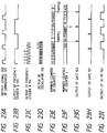
- Fig. 16A shows output signals of the comparator.
- Fig. 16B is a flowchart showing actions to write a set value of the reference voltage to the memory, which are executed before the delivery.
- Fig. 16C is a flowchart showing actions to set the reference voltage after the delivery.
- Th indicates a time for which the pulse of the output signal 303 remains High (i.e., a pulse width at the High level).
- the symbol Tl indicates a time for which the output signal 303 remains Low (i.e., a pulse width at the Low level).
- a reference voltage is sequentially set through the D/A converter while measuring a pulse duty ratio. The setting is ended just when the duty ratio falls within a predetermined range. The reference voltage is automatically set so that a difference between Th and Tl is equal to or within a predetermined value. For this setting, the carriage is moved in step S31. The action proceeds to next step S32.
- step S33 is whether or not an absolute value obtained by subtracting Tl from Th is equal to or smaller than a predetermined value Ttyp. If equal to or smaller than it, it may be judged that a proper reference voltage is present. No adjustment is required. The action therefore proceeds to step S34, wherein the output voltage of the temperature measuring portion is transferred to the compensator.
- step S35 set values of the temperature (actually, the output voltage of the temperature measuring portion) and of the reference voltage are stored in the memory.
- step S36 the carriage is returned to a home position, thus finishing the adjustment.
- step S33 if the difference exceeds the predetermined value Ttyp in step S33, the action goes to step S37. Whether or not Th > Tl is judged therein.
- Th > Tl the set value of the reference voltage inputted to the D/A converter is increased in step S38. Further, when Th ⁇ Tl, the set value of the reference voltage inputted to the D/A converter is decreased in step S39.
- the action goes back to step S32 in order to set a proper reference voltage.
- the action is ended.
- Fig. 16C The data shown in Fig. 16C are stored in the memory according to the steps described above. Note that the graphic chart of Fig. 17 showing the relationship of the MR element output versus the temperature corresponds to Fig. 15A.
- Fig. 16C shows the actions to set the reference voltage in a delivered product after the actions to write the set value of the reference voltage to the memory which have been explained in Fig. 16B.
- step S41 the output voltage of the temperature measuring portion is obtained.
- the output voltage acquired in step S41 is A/D converted in step S42.
- the reference voltage set value stored in the memory is read and D/A converted, thereby setting a reference voltage.
- the following is the way of setting an in-use reference voltage of the actual product. For instance, in a range from a temperature Tk to a temperature Tk+1 shown in Fig. 15B, the output voltage Vok of the temperature measuring portion is inputted to the A/D converter 601 (see Fig. 14) of the compensator.
- the reference voltage Vsk corresponding to the output of the A/D converter is read from the memory 602 and outputted as a reference voltage via the D/A converter 603.
- a combination of TTl semiconductors such as a counter function, a comparator function, etc., or by the software involving the use of a microcomputer, etc.
- the A/D converter, the D/A converter and the memory are employed in the compensator 109.
- the compensator 109 is not limited to these elements but may involve the use of an OP amplifier or the like. Note that printing with a much higher accuracy is attainable in the former case, whereas the costs increase. Further, in the latter case, through the necessary accuracy slightly declines, the costs can be reduced down by using inexpensive parts. Besides, the necessity for control of a CPU is eliminated, and hence the apparatus undergoes no restriction when mounted.
- Fig. 15B shows the output voltage, as expressed in Fig. 15B, of the temperature measuring part.
- Fig. 15A shows the compensator 109 in this instance.
- This compensator is conceived as a so-called non-inversion amplifier circuit, wherein a degree of amplification is adjusted at a ratio of Rf to Rs.
- the duty change is eliminated by the method of varying the reference voltage 302 of the comparator.
- the present invention is not confined to this but may adopt a method of varying the output signals of the magnetic detecting element.
- This embodiment is configured by a circuit shown in Fig. 20.
- the compensator 159 inverts the output of the temperature measuring portion 160 and, in accordance with a signal thereof, functions to amplify the signal of the magnetic detecting element.
- Fig. 18B illustrates the compensator 159 in this case.
- This compensator may be a so-called inversion amplifier circuit consisting of an OP amplifier and a differential amplifier circuit, wherein the output is adjusted at a ratio of Rf to Rs.
- the first through sixth embodiments of the present invention provide the construction, wherein the duty ratio of the printing synchronous output signal pulse waveform is observed, and the synchronous output generation reference voltage is controlled based on the result thereof. It is thus possible to obtain the serial printer capable of high-quality printing owing to the synchronous output which is stable at all times.
- Fig. 21 is a circuit diagram illustrating a configuration of a synchronous signal generating circuit according to this invention.
- the scale portion of the linear encoder is mounted in the carriage shown in Fig. 1 and fixed to the apparatus body.
- a detecting portion 101 of the linear encoder detects a relative moving position of the carriage to the apparatus body by detecting the scale portion.
- the detecting portion 101 is constructed of MR elements which act based on the magnetic resistance effect.
- the detecting portion 101 is provided integrally with a pair of magnetic detecting elements 102, 103. This detecting portion 101 is also connected to the substrate 5 mounted on the carriage, the substrate being shown by a broken line in the Figure.
- the amplifiers 104, 105 for constituting constant current circuits, the amplifier 106 for amplifying a detected signal and the comparator 107.
- the output signal 303 is thereby outputted.
- This output signal is inputted to a counter portion 7.
- a variable resistor 158 for determining a reference voltage is connected to this comparator 107; these elements are packaged on the substrate 5; and an adjustment is made on the carriage.
- Fig. 22 is a diagram showing detailed circuitry of the counter portion 7 shown in Fig. 21.
- a frequency divider A109 consisting of trigger flip-flops effects a 1/2 frequency division with respect to an output of the comparator 107.
- an output signal of an oscillator 113 is inputted to a frequency divider B114.
- Respective output signals of the frequency dividers A109, B114 and the oscillator 113 are inputted to add/count-back counter I115 and an add/count-back counter J116 such as TTL, etc. via gates 110, 111, 112, 115, 116, 117, 119, respectively.
- the magnetic detecting elements 102, 103 are supplied with a constant current via the amplifiers 104, 105 each constituting the constant current circuit.
- the magnetic head 502 moves along the scale portion 501 of the linear encoder illustrated in Fig. 1. Resistance values of the magnetic detecting elements 102, 103 vary with the movement thereof. Variations thereof are detected as fluctuations in voltage.
- a signal amplified by the amplifier 106 is inputted to one input terminal of the comparator 107.
- the output signals 303 (Fig. 23A) of the comparator are converted into high and low clocks (Fig. 23B) per waveform by means of the frequency divider 109 of Fig. 22.
- a pulse (Fig.
- the add/back-count counter 115 counts back the count number down to 0 in a time which is one-half of the time of addition. Further, the add/back-count counter J118 is, as illustrated in Fig. 23F, in the adding process when the output signal of the frequency divider A109 is at the Low level but in the back-counting process when at the High level.
- the counters I, J are counted back after the addition has been executed.
- the counters I, J set ripple clock output signals at the Low level.
- a gate 123 serves to, when any one of the counters I, J gives forth a ripple clock output, invert this output as shown in Fig. 23G. The inverted one is outputted to an input terminal K of a JK-flip-flop 124.
- D-flip-flops 119, 120 and a gate 121 output, to an input terminal J of the JK-flip-flop 124, a signal which assumes the High level at a rise of an output signal 108 of the comparator but, as illustrated in Fig. 23H, the Low level after one clock of the oscillator 113.
- the JK-flip-flop 124 outputs a signal which becomes, as shown in Fig. 23I, the High level at a rise of the gate 121 but the Low level at a rise of the gate 123.
- the JK-flip-flop 124 is thus capable of outputting the clocks exhibiting a duty ratio 50%.
- TTLs 191 are used by ones in the counters, however, if two or more stages are provided, the duty ratio approximates 50%.
- two stages of TTLs 191 are employed, and a clock of the oscillator is set on the order of 500 ns.
- the clock of the output signal of the comparator is on the order of 160 ⁇ s, and, therefore, clocks 1 ⁇ s of the output signals of the frequency divider B can be counted 160.
- the counter is capable of counting 8 bits (256), and this is therefore a sufficient value.
- the circuit and the components (counters, frequency dividers, etc.) in the embodiment are provided by way of one example, but the embodiment is not limited to those components if the same functions are incorporated therein.
- the present invention is oriented to the counter for setting the duty ratio at 50%.
- a noise filter circuit is used in place of the counter.
- Fig. 24 shows one example of the noise filter circuit.
- D-flip-flops 201, 202 and gates 203, 204, 205 are circuits for detecting leading and trailing edges of the output signal 303 of the comparator and generating pulses.
- the three gates 203, 204, 205 (AND circuit, NAND circuit and OR circuit) can be substituted with a single piece of EX-NOR (exclusive NOR) circuit.
- EX-NOR exclusive NOR
- a delay circuit 206 can be easily actualized by connecting the D-flip-flops in series at multi-stages. However, the delay circuit 206 is required to have a delay time larger than a noise pulse width. If a comparator output signal shown in Fig.
- pulses shown in Fig. 25C are obtained from the delay circuit 206.
- a D-flip-flop 207 latches the output signal of the comparator at a rise of this pulse and outputs this output signal (Fig. 25B).
- the noises can be filtered off based on the circuitry described above.
- circuit shown in Fig. 24 is given by way of one example, but other circuitry may be adopted. For instance, the following arrangement may be adopted.
- the D-flip-flop 207 is replaced with a T-flip-flop, and the outputs of the gate 205 is counted by the counter. Only in the case of an odd number (low-order 1-bit output assumes the High level), the pulses are transmitted to the T-flip-flop.
- the counter portion for measuring the wavelength of the synchronous output signal is provided, whereby the duty ratio of the synchronous output signal pulse waveform is set to 50%. It is thus possible to obtain the serial printer capable of high quality printing.
- the filter circuit for filtering off the noises which may probably enter the synchronous signal generating circuit. There is acquired the serial printer which can thereby get the synchronous signal output pulses with no mistake in counting due to the noises.
- Fig. 26 is a basic block diagram of a ninth embodiment.
- a magnetic head 502 reads a magnetic pattern of the scale portion and converts it into an electric signal.
- the magnetic head 502 consists of MR elements.
- the magnetic head 502 outputs a pseudo sine wave signal having a waveform similar to a sine wave with a relative movement to the scale portion. This output signal has two outputs assuming first and second phases, mutually shifted 90 degrees, for detecting a moving direction of the carriage.
- a constant current circuit 312 supplies the magnetic head 502 with a constant current.
- An amplifier 311 amplifies a signal of the magnetic head up to a predetermined magnitude. Parts generally indicated at 502, 301, 302 are mounted on the substrate 5 (see Fig. 1) on the carriage.
- a comparator 313 converts an output signal of the amplifier 311 into a pulse signal.
- the base voltage (reference voltage) of the comparator 313 is given by an output of a D/A converter 314.
- the base voltage is freely variable according to a command of a controller 319 which will be mentioned later.
- a position counter 315 counts information indicating a position of the carriage with respect to the scale portion from a phase lead-to-lag relationship between a first phase pulse signal and a second phase pulse signal as well as from the number of second phase pulses.
- a duty detecting circuit 316 detects duties of the first and second phase pulse signals.
- a thermistor 317 disposed in a proper position (preferably close to the magnetic head) of the substrate 5 is intended to measure a temperature of this part.
- An A/D converter 318 converts an output voltage of the thermistor 317 into a digital value.
- the controller 319 is constructed of a CPU, a ROM, a RAM, I/O ports and a timer circuit.
- the I/O ports are employed for inputting and outputting to and from the D/A converter 314, the position counter 315, the duty detecting circuit 316 and the A/D converter 318.
- the timer circuit is used for generating a timing signal of interruption processing.
- Fig. 27 shows an example of a specific circuit of the position counter.
- the numeral 400 represents a D-FF
- 401 denotes an up-down counter.
- the phases of the first and second phase pulse signals are shifted 90 degrees. It is therefore to know which direction the carriage moves from the phase lead-to-lag relationship therebetween. Thereupon, the phase lead-to-lag relationship is detected by the D-FF.
- An output thereof is connected to an up-down input terminal. For example, the number of the second (or first) phase pulses is counted. Accordingly, when the carriage moves in a certain direction, the pulse number is counted up. Further, when the carriage moves in the direction opposite thereto, the pulse number is counted down. The present position of the carriage is therefore obtained from the count number of the up-down counter.
- a home position sensor 402 involves the use of a photo interrupter.
- the light incident on a light receiving element from a light emitting element of the photo interrupter is cut off.
- a signal is then transmitted to a clear input of the up-down counter 401, thereby zero-clearing the count of the up-down counter 401.
- the count number of the up-down counter 401 indicates a moving distance of the carriage from the home position, i.e., a carriage position.
- Fig. 28 shows a specific example of the duty detecting circuit 316.
- the circuit shown in Fig. 28 detects a duty of the pulse signal assuming one of phases.
- one additional circuit similar thereto is prepared (incidentally, though not illustrated in Fig. 26, for obtaining the pulse signal assuming another phase, there are prepared another set of the magnetic head 502, the amplifier 311, the constant current circuit 312 and the comparator 313; and, as explained earlier, the pulse signals coming from the two comparators are inputted to the position counter 315).
- the pulse signal is at first synchronized with a clock period of a clock circuit 520 by means of a 1st-stage D-FF 521.
- the clock period selected is well faster than the period of the pulse signal outputted with the movement of the carriage.
- the clock period to be selected ranges from several 100 nSec to several ⁇ Sec (several 100 KHz - several MHz).
- the clock circuit 500 may be independently provided. Normally, however, a CPU clock within the controller 319 is usable as it is or by properly dividing the frequency.
- An AND circuit 522 takes a logic product between an output of the D-FF 521 and an output of the clock circuit. The result thereof is counted by a counter 523 having a predetermined number of bits. Counting continues for a duration of a High-state of the pulse signal. More specifically, only when the pulse signal is at the High level, the AND circuit 522 permits the clocks to pass therethrough. The counter 523 counts the number of clocks. When the logic of the pulse signal is inverted, videlicet, when becoming Low, a content of the counter 523 is transferred to a D-latch circuit 507 having a predetermined number of bits while synchronizing with a next leading edge of the clock output through a D-FF 524 and an AND circuit 505.
- the content of the counter 523 is cleared through the D-FF 524 and a negative logic AND circuit 506 when the clock output becomes Low next.
- a negative logic AND circuit 506 when the pulse signal assumes the Low level, an output Q ⁇ of the D-FF 521 becomes High, and hence an output Q ⁇ of the D-FF 524 turns out Low.
- the output of the negative logic AND circuit 506 becomes Low.
- This Low output is inputted to a clear input of the counter, thereby clearing the counter 523.
- a Low output of the negative logic AND circuit 506 is also inputted to a clear input of the D-FF 524, thereby clearing the D-FF 524 itself.
- the content of the D-latch circuit 507 is not therefore updated till the next counting action of the counter 523 is finished (till the pulse signal assumes the Low level after the end of the next counting action for a High-period of the pulse signal). A time-interval of a High duty of the pulse signal is thus measured.
- a time-interval of a Low duty of the pulse signal is measured through an AND circuit 509, a counter 510, a D-FF 512, a negative logic AND circuit 513 and a D-latch circuit 514.
- the controller 319 is capable of reading contents of the D-latch circuits 507, 514 and the latest High and Low duty time-intervals of the pulse signals at arbitrary timings.
- An execution of this action at a predetermined interval is easily attainable by a method in terms of software involving an interrupt processing function of the CPU within the controller 319.
- a moving velocity can be also calculated by dividing a difference between the contents of the counter by an interval time per interval.
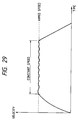
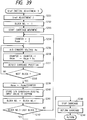
- Fig. 29 is a diagram showing a moving velocity of the carriage.
- the carriage gradually increases the velocity and, when reaching an aimed velocity, moves substantially at a constant velocity.
- the carriage after moving a predetermined distance, gradually decreases the velocity and then stops.
- the duty detecting circuit 316 reads a duty time and calculates a duty ratio. Then, an output (reference voltage inputted to the comparator 313) of the D/A converter 314 is varied based on the result thereof. If the duty ratio does not reach substantially 50% in this state, the duty ratio is re-calculated, and the output of the D/A converter 314 is varied. The steps described above are repeated till the duty ratio comes to substantially 50%.
- the carriage When the duty ratio reaches substantially 50%, the carriage is returned to the home position.
- a temperature at this time i.e., the output of the A/D converter 318, is read and stored in the RAM of the controller 319. Note that the step enters a standby action after the carriage has gone back to the home position.
- the duty ratio may be calculated each time per pulse signal.
- Temperature information is monitored at a predetermined interval.
- this is compared with temperature information stored beforehand. Then, if a temperature difference is a predetermined value or greater, a series of the same actions as those executed when turning ON the power source are performed.
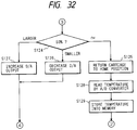
- Figs. 30 - 32 are flowcharts in which contents of the control explained above are rearranged. Next, the contents of the control will be explained referring to these flowcharts. However, the contents of principal actions have already been stated, and therefore only an outline will be given herein.
- step S101 After turning ON the power source, the D/A converter 314 is set to the initial value (step S101). Next, the carriage is moved (step S102), and there is a wait till the carriage reaches a constant speed (step S103). After reaching the constant speed, as explained with reference to Fig. 28, the duty ratio is calculated (step S104).
- step S105 Judged is whether the calculated duty ratio is greater or smaller than or substantially equal to 50% (e.g., within a range of 50% ⁇ 3%) (step S105). If larger than 50%, the output of the D/A converter 314 is increased (step S108). Whereas if smaller, the output of the D/A converter 314 is decreased (step S107). Thereafter, the action goes back to step S102. The steps S102 - S108 or S107 are hereafter repeated till the duty ratio comes to substantially 50%.
- step S105 if the duty ratio is judged to be substantially 50%, the carriage is returned to the home position (step S106). Subsequently, a temperature is read by the A/D converter (step S109) and stored in the RAM of the controller (step S110). Note that the carriage comes to a standby state in the home position.
- step S111 judges next is whether an indication of the recording action is given or not, i.e., during the recording action or the standby status.
- step S112 determines whether the carriage moves at the constant speed or not. If not at the constant speed, actions of steps S111, S112 are repeated till the constant speed is reached.
- step S113 the duty ratio is calculated (step S113). There is judged whether the duty ratio is larger or smaller than or equal to substantially 50% (step S114). If larger than 50%, the output of the D/A converter is increased (step S115). Whereas if smaller, the output of the D/A converter 314 is decreased (step S116).
- step S117 a temperature of read by the A/D converter 318 (step S117) and stored in the RAM of the controller (step S118). Note that if the duty ratio is judged to be substantially 50% in step S114, the action returns to step S111.
- step S119 If the carriage is judged to be in the standby status in step S111, the A/D converter 318 reads a temperature at a predetermined interval (step S119). Judged next is whether or not a difference between the temperature read this time and the temperature read last time is smaller than a predetermined value (step S120). If smaller than the predetermined value, the action goes back to step S111. Whereas if larger than the predetermined value, the carriage is moved (step S121), and there is a wait till the carriage reaches the constant speed (step S122). The duty ratio is then calculated (step S123).
- step S124 there is judged whether the calculated duty ratio is greater or smaller than or equal to substantially 50% (step S124). If larger than 50%, the output of the D/A converter is increased (step S127). Whereas if smaller, the output of the D/A converter 314 is decreased (step S126). Thereafter, the action goes back to step S121. The steps S121 - S127 or S126 are hereafter repeated till the duty ratio comes to substantially 50%.
- step S124 if the duty ratio is judged to be substantially 50% (e.g., within a range of 50% ⁇ 3%), the carriage is returned to the home position (step S125).
- a temperature is read by the A/D converter 318 (step S128) and stored in the RAM of the controller (step S129). Note that the carriage is brought into the standby status in the home position.
- the carriage when the temperature difference larger than the predetermined value is produced during the standby status, the carriage is, as can be understood from the steps S120, S121, automatically moved.
- this becomes troublesome For instance, it is not desirable that the carriage automatically starts moving when the user replaces an ink cartridge employed for recording during the standby status.
- a possible measure is to change the design so that the ink cartridge is allowed to be replaced only for an OFF-time of the power source. In some cases, however, such a measure can not be taken depending on a construction of an appliance.
- an in-standby process is modified as follows.
- the controller 319 judges, when trying to perform an event (e.g., a resumption of the recording action) to move the carriage next, whether or not the carriage is to be moved. If not moved, the carriage reverts to the standby status to prevent the movement of the carriage. Further, only when the carriage is to be moved, a series of the same actions as those when entering the power-ON state are carried out.
- an event e.g., a resumption of the recording action
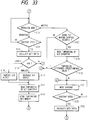
- Fig. 33 is a flowchart in which the modified contents of the control explained above are rearranged.
- step S111 if judged to be the standby status in step S111, there is judged whether the event to move the carriage happens or not (step S150). If the event does not happen, the action goes back to step S111. Whereas if it is judged that the event happens, the A/D converter 318 reads a temperature (step S151). Whether or not a difference between the read temperature of this time and the read temperature of the last time is smaller than a predetermined value (step S152). If the temperature difference is smaller than the predetermined value, the action returns to step S111. If larger, the action proceeds to step S121. There is hereafter conducted the control of the same actions of steps S122 - S125, S126 or S127 as those in the power-ON state.
- the carriage in the standby status is by no means moved in an uncontrolled manner (i.e., as far as there happens no event to move the carriage as by a command of recording action, the action does not proceed to step S121 wherein the carriage is moved). It is therefore possible to prevent the trouble which may take place when replacing the ink cartridge.
- the control to set the duty ratio at 50% is conducted beforehand just when the carriage reaches the constant moving speed in the power-ON state. Hence, the highly accurate duty ratio 50% is quickly obtained. Even when shifting to the recording action, the recording action can be easily performed at the duty ratio 50% which gives a desirable printing result from the beginning. Besides, there is executed the control to set the duty ratio at 50% at all times when the carriage reaches the constant moving speed during the recording action also. The duty ratio can be therefore always kept at 50% during the recording action.
- the control to keep the duty ratio at 50% is performed.
- the recording action can be quickly executed at the duty ratio 50%.
- Fig. 34 is a block diagram illustrating a configurational example of the circuit of the serial printer shown in Fig. 1.
- the scale portion of the magnetic linear encoder is mounted in the carriage and fixed to the apparatus body.
- the magnetic linear encoder includes a detecting portion 101 for detecting a relative moving position of the carriage by detecting information which is magnetized on the scale portion.
- the detecting portion 101 incorporates magnetic detecting elements 102, 103 consisting of MR elements which act based on the magnetic resistance effect.
- the detecting portion 101 is also connected to a carriage substrate 5 (indicated by a broken line in Fig. 1) mounted on the carriage.
- This carriage substrate 5 includes a constant current circuit 104 and a differential amplifier 106 for differentially amplifying respective signals detected by the detecting elements.
- An output signal A O (or 108) is outputted from the differential amplifier 106.
- a printer control circuit substrate 4 includes an A/D converter 132 for A/D converting the output signal A O and a comparator 130 for generating a counter pulse A (or 131) having a pulse waveform by comparing the output signal A O with a reference voltage.
- the printer control circuit substrate 4 also includes a D/A converter 134 for generating a reference voltage V ref (or 140) defined as an input signal to one terminal of the comparator 130 and a counter/timer 133 for counting counter pulses A.
- the printer control circuit substrate 4 further includes a CPU 135 for controlling the system, an EEPROM 136 serving as a memory device, a ROM 137, a RAM 138 and a CPU bus 139 serving as a bus for data, addresses and control signals of the CPU 135. Note that some or the whole of the components surrounded with the broken line may be incorporated into the CPU 135.
- the magnetic detecting elements 102, 103 are supplied with a constant current via the constant current circuits 104, 105, respectively.
- Magnetic patterns are previously magnetized at a fixed interval on the scale portion 501 (see Fig. 1), fixed to the apparatus body, of the magnetic linear encoder.
- resistance values of the magnetic detecting elements 102, 103 vary. Variations in the resistance values are detected as fluctuations in voltage.
- amplification signals thereof are inputted to one input terminal of the comparator 130.
- the output signal A O transmitted from the differential amplifier 106 is a pseudo sine wave and therefore compared with the reference voltage V ref outputted from the D/A converter 134 in the comparator 130.
- the counter pulses A are thereby obtained as synchronous signals.
- the counter pluses A are inputted to and counted by the counter/timer 133.
- a count value thereof represents a position of the carriage.
- the CPU 135 controls the system and transfers the data of the EEPROM 136, the ROM 137 and the RAM 138 via the CPU bus 139.
- the CPU 135 also controls the A/D converter 132, the counter/timer 133 and the D/A converter 134.
- the CPU 135 further controls other functions (e.g., an interface function to the host control over a variety of motors, a printing action, etc.) of the serial printer.
- the output signal A O obtained from the detecting portion of the magnetic linear encoder is the pseudo sine wave. It is therefore required that the output signal be converted into the counter pulse A expressed by the digital signal (pulse waveform) by use of the converter 130.
- the reference voltage V ref inputted to the comparator employed for the conversion and compared with the output signal A O is desirably an average value of the output signals A O . For this reason, an initial adjustment is, it is required, made so that the reference voltage V ref becomes the average value of the output signals A O .
- step S221 the carriage starts moving (step S221).
- the counter pulse from the linear encoder is not yet correctly outputted at this moment, and, hence, the moving speed is unknown. Accordingly, there is previously obtained the minimum torque by which to shift a load based on mechanism parts such as the carriage and the guide shaft member.
- the CPU issues a command to move the carriage at a velocity so that the carriage motion is not so fast.
- the output signals A O from the differential amplifier 106 are detected.
- Outputted to the D/A converter 134 is such a digital value that the average value of the output signals A O becomes the reference voltage V ref (step S222).
- step S222 the carriage is returned to the initial position (step S223).
- step S222 the content of step S222 will be explained in greater detail with reference to Fig. 36B.
- the number n an integer of 1 or larger predetermined as a measurement number of the output signals A O is initialized in the counter.
- an addition area A sum of A O is cleared (step S211).
- data A O is A/D converted by the A/D converter 132 and thereafter taken in the RAM 138 (step S212).
- the counter is decremented, and at the same time, A O is added to A SUM (step S213).
- step S214 whether or not the counter is 0 is judged (step S214). If not 0, the action goes back to step S212. If the counter is 0, the action proceeds to step S215.
- a sequence of the initial adjustment of V ref is normally performed once before delivering the serial printer from the factory. However, if the output A O largely changes with a passage of time, a sequence of the V ref initial adjustment may be incorporated in the initialization sequence after turning ON the power source when used. As stated earlier, the digital value stored in the EEPROM is set in the D/A converter in the initialization sequence after the power-ON process of the serial printer.
- step S224 the carriage is moved again.
- steps S225 - S227 will be executed. These steps, however, form a carriage speed control loop.
- the carriage speed is detected (step S225). Whether or not the carriage speed is synchronized is judged (step S226). If not synchronized, the carriage speed is adjusted (step S227). The action goes back to step S225, wherein the carriage speed is detected once more. Whether or not the carriage speed is synchronized is judged again. Steps S225 - S227 are repeated till the carriage speed is synchronized. When synchronized, the action proceeds to the next step, i.e., step S228.
- the carriage speed adjustment in step S227 involves a step of reading a count value of the count pulses A from the counter/timer.
- the carriage speed is adjusted to establish the following relational formula 1 wherein a sampling period T S of the A/D converter is expressed in relation to a period of the output A O of the MR element.
- T S T AO / 2 m (m is the integer of 1 or greater) (1)
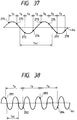
- Fig. 37 shows an example where the relational formula 1 is established.
- T S is variable
- only T S may be varied to establish the relational formula 1 without changing T AO , i.e., without changing the moving speed of the carriage.
- step S228 A O is measured n-times at a T S -interval, thus calculating the average value A ave .
- the average value A ave of the measurement effected n-times is equal to a DC component of A O .
- sampling may be effected at such a timing that a phase of A O is shifted 180 degrees. It can be comprehended from the example of Fig. 37 that values of points 271 - 273, 272 - 274, 275 - 277 and 276 - 278 offset errors with respect to the DC level of A O .
- the carriage moving speed is synchronized with the sampling period of the A/D converter with respect to the MR element output.
- the counter pulse can be thereby obtained, wherein the duty ratio is approximate to 50%.
- the variations in the counter pulse waveform due to the passage-of-time change in the MR element output can be restrained.
- a scatter in density as a result of recording by the serial printer can be thereby restrained.
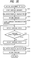
- Fig. 39 is a flowchart (V ref initial adjustment 3) showing actions of a reference voltage V ref initial adjusting method in the serial printer according to this invention. Note that the hardware of the serial printer is the same as that shown in Figs. 1 and 34, and its explanation is omitted herein.
- step S231 the steps (steps S221 - S229 shown in Fig. 35) of the V ref initial adjustment 2 described above are at first executed (step S231).
- a block number 1 is set, videlicet, the block number is initialized (step S232).
- the carriage starts moving (step S233).
- the add counter of A O and the addition area A SUM are initialized (step S234).
- the A/D converter measures the voltage A O (step 235).
- the add counter is incremented (1 is added), and, besides, A O is added to A SUM (step S236).
- a carriage position is detected through the counter/timer (step S237).
- step S2308 whether or not the carriage position reaches the next block is judged.
- the block herein implies one unit when a carriage moving range is previously partitioned into blocks at an interval.
- the above-mentioned block number implies a serial number put on each block which is incremented as the carriage moves.
- steps S235 - S237 are repeated till the next block is reached.
- step S2308 if it is judged that the carriage position reaches the next block, A SUM is divided by the add counter to calculate the average value A ave (step S239).
- a digital value is stored in an area, corresponding to the present block number, of the EEPROM. this digital value being set in the D/A converter as the average value A ave in the carriage position indicated by the thus obtained present block number, i.e., as the reference voltage V ref (step S240).
- step S242 if it is judged that the present block number is not larger than the final block number, steps S234 - S242 are repeated till the present block number becomes larger than the final block number. In this manner, the average value A ave per block is stored in each corresponding area of the EEPROM. Then, in step S242, if it is judged that the present block number is larger than the final block number, the carriage stops (step S243). The carriage is returned to the initial position (step S244).
- Fig. 40 is a timing chart showing relationships of the carriage position versus the output signal A O from the differential amplifier 106, the ideal reference voltage V ref defined as the DC component of A O , an ideal counter pulse A(a) in this instance, a counter pulse A(b) when the average value of A O in the entire carriage moving range is V ref and a counter pulse A(c) when an in-block average value of A O is V ref .
- V ref the ideal reference voltage
- step S231 of Fig. 39 the counter pulse A can be, though it does not take an ideal waveform as shown by A(b) in Fig. 40, obtained enough for block partitioning of the carriage position.
- One block may be set well longer than a period (e.g., 360 dpi) of the counter pulse A.
- a positional accuracy of a block boundary may also be set considerably lower than a carriage position detecting accuracy needed during the printing process. Accordingly, the counter pulse A at the end of step S231 may not be so accurate.
- the block number is initialised in step S232.
- the carriage starts moving in step S233.
- the A and the addition area A SUM are initialized.
- a O undergoes periodic sampling till the carriage position exceeds a range of the present block number, and an addition thereof is applied to A SUM .
- the A O average value A ave in the present block number is thus obtained in step S239.
- the block number is incremented in step S241.
- the present block number is compared with the predetermined final block number (4 in the embodiment in Fig.
- step S242 When the present block number does not exceed the final block number, steps S234 - S242 are repeated.
- the digital value set in the D/A converter is therefore sequentially stored in the EEPROM, with A O average value in each block being V ref . After the V ref digital values in all the blocks have completely been stored in the EEPROM, the carriage stops in step S243. The carriage is returned to the original position in step S244.
- (c) shows the counter pulse A when V ref is varied stepwise in accordance with the carriage position so that the in-block A O average value is V ref .
- This is approximate to the ideal waveform A(a) as compared with the waveform A(b) when V ref is the A O average value in the entire carriage moving range.
- the number of blocks may be set to an optimum value depending on an amount of fluctuation in the DC component of A O as well as on an allowance of the areas in the EEPROM. For instance, if the amount of fluctuation in the DC component of A O is large, and when there are sufficient empty areas of the EEPROM, the number of blocks is preferably large (finer blocks). In general, the blocks are arranged preferably at equal spacings but may be, if there is some allowance for areas of the EEPROM, arranged at unequal spacings. In this case, it is required that the carriage position at the block boundary be also stored in the EEPROM. This is effective in such an instance that the DC component of A O locally fluctuates.
- Fig. 41 is a flowchart showing printing for one line in such a case.
- steps S251 - S252 and steps S258 - S260 are added by way of the thirteenth embodiment of this invention.
- Other steps are the same as those shown in Fig. 36A.
- step S251 1 is set as a block number, i.e., the block number is initialized.
- step S252 the reference voltage V ref corresponding to the block number 1 is set in the D/A converter.
- step S253 the carriage starts moving.
- the carriage speed is set at a predetermined velocity in a loop formed by steps S254 - S256. More specifically, the carriage speed is detected in step S254. Whether or not the carriage speed is the predetermined velocity is judged in step S255. If not the predetermined velocity, the carriage speed is controlled in step S256. The action thereafter goes back to step S254. Steps S254 - S256 are repeated till the predetermined velocity is reached. Subsequently, in step S257, printing is effected in a predetermined position.
- Step S258 the carriage position is detected.
- Steps S259 - S261 are to detect which block the carriage now exists and to reset, if over the block boundary, the reference voltage V ref in accordance with the block number.
- step S262 whether one-line printing has been finished or not is judged. If not finished, steps S257 - S262 are repeated. Whereas if finished, the carriage stops in step S264. A line feed is performed in step S265.
- steps S251, S259, S260 in the flowchart of Fig. 41 may be modified as below in the case of bidirectional printing.
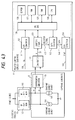
- Fig. 43 is a circuit block diagram in the fourteenth embodiment.
- the circuit shown in Fig. 43 has an addition of a data selector 142 in contrast with the circuit illustrated in Fig. 34.
- Other configurations are the same, and hence the following explanation is centered on the data selector 142.
- the portions relative to other configurations have already been explained, and, hence, the descriptions thereof are omitted.
- D/A converter set data for a plurality of blocks which have been written from the CPU 135 are selected by the data selector 142 in accordance with a selector signal 143 coming from the counter/timer 133.
- the selected data are set in the D/A converter 134.
- the corresponding-to-carriage-position setting of V ref can be thereby conducted without increasing a load in terms of software, i.e., in accordance with the flowchart exclusive of steps S251 - S252 and steps S258 - S261 in the 1-line printing flowchart of Fig. 41.
- the digital data of V ref in each block which is obtained in the embodiment of Fig. 39 is previously set in the data selector 142 before the printing action as an initial state before the printing action.
- the counter/timer 133 is connected to the data selector 142, whereby the carriage position counter data for high-order several bits corresponding to each block are transferred in the form of the selector signal 143 from the counter-timer 133 to the data selector 142.
- the selector signal 143 For example, when the division number of blocks is set to 4, two or three bits may suffice for the selector signal 143.
- the carriage position counter within the counter/timer 133 counts up and down correspondingly, with the result that the selector signal 143 changes.
- An item of V ref digital data 144 imparted to the D/A converter 134 is changed over by the data selector 142.
- the data selector 142 may be so constructed as to be capable of storing a plurality of items of data, selecting one item of the data with the aid of the selector signal and outputting it. Accordingly, an arrangement may be taken, wherein the data selector involves the use of, e.g., a dual port RAM, and the selector signal is connected to an address of one port.
- an output 140 of the D/A converter 134 may be inputted via a low-pass filter (unillustrated) to the comparator 110.
- the software for previously measuring and storing the reference voltage V ref corresponding to the carriage position is provided also is the software or hardware for selecting in real time the reference voltage V ref stored corresponding to the carriage position during the printing action. It is therefore possible to obtain the counter pulse exhibiting the good state over the entire carriage moving range and defined as an output of the comparator. This is attained even when the DC component of the output of the differential amplifier which is inputted to the comparator largely varies due to the carriage position. Consequently, the carriage position detecting accuracy can be improved. A resultant quality of recording by the serial printer can be also ameliorated.
- the waveform of the counter pulse can be approximate to the ideal waveform when the duty ratio is 50%.
- a sufficient allowance is therefore provided against the passage-of-time change in the output of the differential amplifier, thereby making it possible to reduce a degree of decline in the printing quality with the passage of time. This implies that a frequency of executing the initial adjustment sequence of the reference voltage V ref may be decreased. A user's feeling in operation is improved.
Landscapes
- Character Spaces And Line Spaces In Printers (AREA)
- Materials For Photolithography (AREA)
- Diaphragms For Electromechanical Transducers (AREA)
- Accessory Devices And Overall Control Thereof (AREA)
- Printers Or Recording Devices Using Electromagnetic And Radiation Means (AREA)
- Measurement Of Length, Angles, Or The Like Using Electric Or Magnetic Means (AREA)
- Manipulation Of Pulses (AREA)
Applications Claiming Priority (10)
| Application Number | Priority Date | Filing Date | Title |
|---|---|---|---|
| JP255956/92 | 1992-08-31 | ||
| JP25595692A JP3152319B2 (ja) | 1992-08-31 | 1992-08-31 | シリアルプリンタ装置 |
| JP04283671A JP3126240B2 (ja) | 1992-09-29 | 1992-09-29 | シリアルプリンタ装置 |
| JP283671/92 | 1992-09-29 | ||
| JP314001/92 | 1992-10-29 | ||
| JP04314001A JP3098121B2 (ja) | 1992-10-29 | 1992-10-29 | シリアルプリンタ |
| JP32486492A JP3297101B2 (ja) | 1992-11-10 | 1992-11-10 | シリアルプリンタ |
| JP324864/92 | 1992-11-10 | ||
| JP12532893A JP3244204B2 (ja) | 1993-04-28 | 1993-04-28 | シリアルプリンタ装置 |
| JP125328/93 | 1993-04-28 |
Publications (3)
| Publication Number | Publication Date |
|---|---|
| EP0585881A2 true EP0585881A2 (fr) | 1994-03-09 |
| EP0585881A3 EP0585881A3 (fr) | 1994-12-07 |
| EP0585881B1 EP0585881B1 (fr) | 1997-11-19 |
Family
ID=27527064
Family Applications (1)
| Application Number | Title | Priority Date | Filing Date |
|---|---|---|---|
| EP93113914A Expired - Lifetime EP0585881B1 (fr) | 1992-08-31 | 1993-08-31 | Imprimante en série |
Country Status (7)
| Country | Link |
|---|---|
| US (1) | US5427461A (fr) |
| EP (1) | EP0585881B1 (fr) |
| KR (1) | KR970003658B1 (fr) |
| CN (1) | CN1035288C (fr) |
| AT (1) | ATE160317T1 (fr) |
| DE (1) | DE69315284T2 (fr) |
| TW (1) | TW226450B (fr) |
Cited By (3)
| Publication number | Priority date | Publication date | Assignee | Title |
|---|---|---|---|---|
| EP0987117A2 (fr) * | 1998-08-31 | 2000-03-22 | Eastman Kodak Company | Commande programmable d'engrenage d'un vis-écrou pour une tête d'impression ayant un nombre de canaux variable |
| EP1043168A2 (fr) * | 1999-04-06 | 2000-10-11 | Alps Electric Co., Ltd. | Imprimante thermique et son procédé d'enregistrement |
| CN100453330C (zh) * | 2005-06-17 | 2009-01-21 | 株式会社理光 | 图像形成装置 |
Families Citing this family (19)
| Publication number | Priority date | Publication date | Assignee | Title |
|---|---|---|---|---|
| US5600352A (en) * | 1994-06-27 | 1997-02-04 | Tektronix, Inc. | Apparatus and method for controlling coalescence of ink drops on a print medium |
| US5774080A (en) * | 1994-12-15 | 1998-06-30 | Analog Devices, Incorporated | Reduced transistor-count data storage and multiplexing system |
| US5739658A (en) * | 1995-03-31 | 1998-04-14 | International Business Machines Corporation | Noise dithering system for transistor switched devices |
| JP3423478B2 (ja) * | 1995-05-30 | 2003-07-07 | キヤノン株式会社 | 記録装置 |
| KR0185048B1 (ko) * | 1996-06-20 | 1999-05-15 | 김광호 | 스텝모터의 위치 제어와 인자헤드의 인자 제어 장치 및 방법 |
| US6166828A (en) * | 1997-07-28 | 2000-12-26 | Canon Kabushiki Kaisha | Clearing ink jet nozzles during printing |
| US6339480B1 (en) | 1997-07-28 | 2002-01-15 | Canon Kabushiki Kaisha | Print driver for a color printer |
| US6283650B1 (en) | 1997-07-28 | 2001-09-04 | Canon Kabushiki Kaisha | Printing device having an output level compensation function |
| EP0938977B1 (fr) * | 1997-09-02 | 2006-06-07 | Seiko Epson Corporation | Imprimante pour impression bidirectionnelle et procede de reglage de la position d'impression |
| JP3501654B2 (ja) * | 1998-07-16 | 2004-03-02 | キヤノン株式会社 | 記録装置 |
| US6609781B2 (en) | 2000-12-13 | 2003-08-26 | Lexmark International, Inc. | Printer system with encoder filtering arrangement and method for high frequency error reduction |
| US6830399B2 (en) * | 2003-03-14 | 2004-12-14 | Lexmark International, Inc. | Methods and systems for compensation of media indexing errors in a printing device |
| JP3988757B2 (ja) * | 2004-07-28 | 2007-10-10 | ブラザー工業株式会社 | モータ制御装置、モータ制御方法、及びプログラム |
| JP2008143091A (ja) * | 2006-12-12 | 2008-06-26 | Canon Inc | インクジェット記録装置およびインクジェット記録方法 |
| CN103029429B (zh) * | 2011-09-30 | 2015-11-25 | 北大方正集团有限公司 | 印刷系统及其色标控制方法 |
| US9835347B2 (en) | 2014-12-08 | 2017-12-05 | Johnson Controls Technology Company | State-based control in an air handling unit |
| JP6631048B2 (ja) * | 2015-06-23 | 2020-01-15 | セイコーエプソン株式会社 | 分光測定装置、画像形成装置、及び分光測定方法 |
| CN108089575B (zh) * | 2016-11-23 | 2021-08-10 | 苏州宝时得电动工具有限公司 | 自移动设备定位装置和方法 |
| JP7154867B2 (ja) | 2018-08-01 | 2022-10-18 | キヤノン株式会社 | インクジェット記録装置、その制御方法およびプログラム |
Citations (11)
| Publication number | Priority date | Publication date | Assignee | Title |
|---|---|---|---|---|
| FR2157187A5 (fr) * | 1971-10-21 | 1973-06-01 | Sagem | |
| EP0157048A2 (fr) * | 1983-11-10 | 1985-10-09 | Hewlett-Packard Company | Appareil de mesure de position |
| US4652159A (en) * | 1984-05-02 | 1987-03-24 | Kabushiki Kaisha Seiko Epson | Printer |
| EP0226449A2 (fr) * | 1985-12-11 | 1987-06-24 | International Business Machines Corporation | Appareil et méthode pour calculer les paramètres d'un système d'entraînement pour une tête d'imprimante d'une imprimante |
| EP0300823A2 (fr) * | 1987-07-23 | 1989-01-25 | Hewlett-Packard Company | Système de positionnement incrémental |
| EP0357526A2 (fr) * | 1988-09-01 | 1990-03-07 | SCITEX DIGITAL PRINTING, Inc. | Méthode de commande de l'accélération d'un assemblage à tête d'impression |
| EP0372844A2 (fr) * | 1988-12-02 | 1990-06-13 | Ncr International Inc. | Méthode de commande d'une imprimante |
| EP0401843A1 (fr) * | 1989-06-09 | 1990-12-12 | Canon Kabushiki Kaisha | Appareil d'enregistrement |
| JPH0375180A (ja) * | 1989-08-18 | 1991-03-29 | Nec Corp | ドットシリアルプリンタ |
| JPH0399874A (ja) * | 1989-09-13 | 1991-04-25 | Nec Corp | 印字ヘッドキャリジ移動制御パラメータの決定方式 |
| JPH03265481A (ja) * | 1990-03-15 | 1991-11-26 | Nec Corp | シリアルプリンタのモータ制御回路 |
Family Cites Families (3)
| Publication number | Priority date | Publication date | Assignee | Title |
|---|---|---|---|---|
| JPS5554429A (en) * | 1978-10-17 | 1980-04-21 | Toshiba Corp | Bearing supervisory unit |
| US4855067A (en) * | 1988-05-10 | 1989-08-08 | Colgate-Palmolive Company | Household cleaning composition |
| JPH04188931A (ja) * | 1990-11-21 | 1992-07-07 | Nec Corp | ラインドライバ回路 |
-
1993
- 1993-08-24 TW TW082106819A patent/TW226450B/zh not_active IP Right Cessation
- 1993-08-30 US US08/113,326 patent/US5427461A/en not_active Expired - Lifetime
- 1993-08-30 KR KR1019930016999A patent/KR970003658B1/ko not_active IP Right Cessation
- 1993-08-31 DE DE69315284T patent/DE69315284T2/de not_active Expired - Lifetime
- 1993-08-31 AT AT93113914T patent/ATE160317T1/de not_active IP Right Cessation
- 1993-08-31 CN CN93117242A patent/CN1035288C/zh not_active Expired - Fee Related
- 1993-08-31 EP EP93113914A patent/EP0585881B1/fr not_active Expired - Lifetime
Patent Citations (11)
| Publication number | Priority date | Publication date | Assignee | Title |
|---|---|---|---|---|
| FR2157187A5 (fr) * | 1971-10-21 | 1973-06-01 | Sagem | |
| EP0157048A2 (fr) * | 1983-11-10 | 1985-10-09 | Hewlett-Packard Company | Appareil de mesure de position |
| US4652159A (en) * | 1984-05-02 | 1987-03-24 | Kabushiki Kaisha Seiko Epson | Printer |
| EP0226449A2 (fr) * | 1985-12-11 | 1987-06-24 | International Business Machines Corporation | Appareil et méthode pour calculer les paramètres d'un système d'entraînement pour une tête d'imprimante d'une imprimante |
| EP0300823A2 (fr) * | 1987-07-23 | 1989-01-25 | Hewlett-Packard Company | Système de positionnement incrémental |
| EP0357526A2 (fr) * | 1988-09-01 | 1990-03-07 | SCITEX DIGITAL PRINTING, Inc. | Méthode de commande de l'accélération d'un assemblage à tête d'impression |
| EP0372844A2 (fr) * | 1988-12-02 | 1990-06-13 | Ncr International Inc. | Méthode de commande d'une imprimante |
| EP0401843A1 (fr) * | 1989-06-09 | 1990-12-12 | Canon Kabushiki Kaisha | Appareil d'enregistrement |
| JPH0375180A (ja) * | 1989-08-18 | 1991-03-29 | Nec Corp | ドットシリアルプリンタ |
| JPH0399874A (ja) * | 1989-09-13 | 1991-04-25 | Nec Corp | 印字ヘッドキャリジ移動制御パラメータの決定方式 |
| JPH03265481A (ja) * | 1990-03-15 | 1991-11-26 | Nec Corp | シリアルプリンタのモータ制御回路 |
Non-Patent Citations (4)
| Title |
|---|
| NEC RESEARCH AND DEVELOPMENT, no.65, April 1982, TOKYO JP pages 16 - 23 INADA ET AL. 'Digital Servo System for Impact Serial Printer' * |
| PATENT ABSTRACTS OF JAPAN vol. 15, no. 239 (M-1126) 20 June 1991 & JP-A-03 075 180 (KAMITSUBARA KINJI) 29 March 1991 * |
| PATENT ABSTRACTS OF JAPAN vol. 15, no. 283 (M-1137) 18 July 1991 & JP-A-03 099 874 (IWAZAWA HISATOSHI) 25 April 1991 * |
| PATENT ABSTRACTS OF JAPAN vol. 16, no. 74 (E-1170) 24 February 1992 & JP-A-03 265 481 (ISHIZAKI SUNAO) 26 November 1991 * |
Cited By (5)
| Publication number | Priority date | Publication date | Assignee | Title |
|---|---|---|---|---|
| EP0987117A2 (fr) * | 1998-08-31 | 2000-03-22 | Eastman Kodak Company | Commande programmable d'engrenage d'un vis-écrou pour une tête d'impression ayant un nombre de canaux variable |
| EP0987117A3 (fr) * | 1998-08-31 | 2002-01-30 | Eastman Kodak Company | Commande programmable d'engrenage d'un vis-écrou pour une tête d'impression ayant un nombre de canaux variable |
| EP1043168A2 (fr) * | 1999-04-06 | 2000-10-11 | Alps Electric Co., Ltd. | Imprimante thermique et son procédé d'enregistrement |
| EP1043168A3 (fr) * | 1999-04-06 | 2001-01-31 | Alps Electric Co., Ltd. | Imprimante thermique et son procédé d'enregistrement |
| CN100453330C (zh) * | 2005-06-17 | 2009-01-21 | 株式会社理光 | 图像形成装置 |
Also Published As
| Publication number | Publication date |
|---|---|
| KR940004492A (ko) | 1994-03-15 |
| US5427461A (en) | 1995-06-27 |
| EP0585881A3 (fr) | 1994-12-07 |
| EP0585881B1 (fr) | 1997-11-19 |
| CN1087736A (zh) | 1994-06-08 |
| DE69315284T2 (de) | 1998-04-02 |
| DE69315284D1 (de) | 1998-01-02 |
| KR970003658B1 (ko) | 1997-03-20 |
| TW226450B (fr) | 1994-07-11 |
| ATE160317T1 (de) | 1997-12-15 |
| CN1035288C (zh) | 1997-06-25 |
Similar Documents
| Publication | Publication Date | Title |
|---|---|---|
| EP0585881B1 (fr) | Imprimante en série | |
| US6838855B2 (en) | Method and apparatus for controlling motor | |
| US5671069A (en) | Pixel clock generator | |
| EP0961119A2 (fr) | Procédé pour le réglage de la vitesse d'un moteur | |
| US6411075B1 (en) | Electronic frequency measuring device and its use | |
| US20120306419A1 (en) | Motor speed controller and control method | |
| US4315198A (en) | Digital servo system | |
| US6170933B1 (en) | Printer control apparatus | |
| EP0945277A2 (fr) | Dispositif d'impression avec générateur d'impulsions d'horloge | |
| JP2002034274A (ja) | ディジタルエンコーダー制御方法 | |
| JPH10178548A (ja) | 入力波形を出力波形に変換する方法 | |
| JP3297101B2 (ja) | シリアルプリンタ | |
| JP4827341B2 (ja) | モータ回転制御装置および画像形成装置 | |
| KR960014321B1 (ko) | 수평발진제어회로 | |
| JP3098121B2 (ja) | シリアルプリンタ | |
| JPH0679943A (ja) | シリアルプリンタ装置 | |
| JP4012661B2 (ja) | 信号生成回路、半導体レーザ駆動制御回路及び画像形成装置 | |
| JP2736583B2 (ja) | モータ速度制御装置 | |
| EP0099977A1 (fr) | Système d'asservissement numérique pour la commande d'un moteur | |
| JP3244204B2 (ja) | シリアルプリンタ装置 | |
| JP2001146054A (ja) | 記録装置 | |
| JPH06255194A (ja) | シリアルプリンタ装置 | |
| JPH11105348A (ja) | 記録装置 | |
| JPS6223763A (ja) | シリアルプリンタの印字タイミング信号生成装置 | |
| JP2674111B2 (ja) | 画像記録装置 |
Legal Events
| Date | Code | Title | Description |
|---|---|---|---|
| PUAI | Public reference made under article 153(3) epc to a published international application that has entered the european phase |
Free format text: ORIGINAL CODE: 0009012 |
|
| AK | Designated contracting states |
Kind code of ref document: A2 Designated state(s): AT BE CH DE DK ES FR GB GR IE IT LI LU NL PT SE |
|
| PUAL | Search report despatched |
Free format text: ORIGINAL CODE: 0009013 |
|
| AK | Designated contracting states |
Kind code of ref document: A3 Designated state(s): AT BE CH DE DK ES FR GB GR IE IT LI LU NL PT SE |
|
| 17P | Request for examination filed |
Effective date: 19950531 |
|
| 17Q | First examination report despatched |
Effective date: 19960530 |
|
| GRAG | Despatch of communication of intention to grant |
Free format text: ORIGINAL CODE: EPIDOS AGRA |
|
| GRAH | Despatch of communication of intention to grant a patent |
Free format text: ORIGINAL CODE: EPIDOS IGRA |
|
| GRAH | Despatch of communication of intention to grant a patent |
Free format text: ORIGINAL CODE: EPIDOS IGRA |
|
| GRAH | Despatch of communication of intention to grant a patent |
Free format text: ORIGINAL CODE: EPIDOS IGRA |
|
| GRAA | (expected) grant |
Free format text: ORIGINAL CODE: 0009210 |
|
| AK | Designated contracting states |
Kind code of ref document: B1 Designated state(s): AT BE CH DE DK ES FR GB GR IE IT LI LU NL PT SE |
|
| PG25 | Lapsed in a contracting state [announced via postgrant information from national office to epo] |
Ref country code: NL Free format text: LAPSE BECAUSE OF FAILURE TO SUBMIT A TRANSLATION OF THE DESCRIPTION OR TO PAY THE FEE WITHIN THE PRESCRIBED TIME-LIMIT Effective date: 19971119 Ref country code: LI Free format text: LAPSE BECAUSE OF FAILURE TO SUBMIT A TRANSLATION OF THE DESCRIPTION OR TO PAY THE FEE WITHIN THE PRESCRIBED TIME-LIMIT Effective date: 19971119 Ref country code: GR Free format text: LAPSE BECAUSE OF FAILURE TO SUBMIT A TRANSLATION OF THE DESCRIPTION OR TO PAY THE FEE WITHIN THE PRESCRIBED TIME-LIMIT Effective date: 19971119 Ref country code: ES Free format text: THE PATENT HAS BEEN ANNULLED BY A DECISION OF A NATIONAL AUTHORITY Effective date: 19971119 Ref country code: DK Free format text: LAPSE BECAUSE OF NON-PAYMENT OF DUE FEES Effective date: 19971119 Ref country code: CH Free format text: LAPSE BECAUSE OF FAILURE TO SUBMIT A TRANSLATION OF THE DESCRIPTION OR TO PAY THE FEE WITHIN THE PRESCRIBED TIME-LIMIT Effective date: 19971119 Ref country code: BE Free format text: LAPSE BECAUSE OF FAILURE TO SUBMIT A TRANSLATION OF THE DESCRIPTION OR TO PAY THE FEE WITHIN THE PRESCRIBED TIME-LIMIT Effective date: 19971119 Ref country code: AT Free format text: LAPSE BECAUSE OF FAILURE TO SUBMIT A TRANSLATION OF THE DESCRIPTION OR TO PAY THE FEE WITHIN THE PRESCRIBED TIME-LIMIT Effective date: 19971119 |
|
| REF | Corresponds to: |
Ref document number: 160317 Country of ref document: AT Date of ref document: 19971215 Kind code of ref document: T |
|
| REG | Reference to a national code |
Ref country code: CH Ref legal event code: EP |
|
| REF | Corresponds to: |
Ref document number: 69315284 Country of ref document: DE Date of ref document: 19980102 |
|
| ITF | It: translation for a ep patent filed |
Owner name: SOCIETA' ITALIANA BREVETTI S.P.A. |
|
| ET | Fr: translation filed | ||
| PG25 | Lapsed in a contracting state [announced via postgrant information from national office to epo] |
Ref country code: SE Free format text: LAPSE BECAUSE OF FAILURE TO SUBMIT A TRANSLATION OF THE DESCRIPTION OR TO PAY THE FEE WITHIN THE PRESCRIBED TIME-LIMIT Effective date: 19980219 Ref country code: PT Free format text: LAPSE BECAUSE OF FAILURE TO SUBMIT A TRANSLATION OF THE DESCRIPTION OR TO PAY THE FEE WITHIN THE PRESCRIBED TIME-LIMIT Effective date: 19980219 |
|
| NLV1 | Nl: lapsed or annulled due to failure to fulfill the requirements of art. 29p and 29m of the patents act | ||
| REG | Reference to a national code |
Ref country code: CH Ref legal event code: PL |
|
| PG25 | Lapsed in a contracting state [announced via postgrant information from national office to epo] |
Ref country code: LU Free format text: LAPSE BECAUSE OF NON-PAYMENT OF DUE FEES Effective date: 19980831 Ref country code: IE Free format text: LAPSE BECAUSE OF NON-PAYMENT OF DUE FEES Effective date: 19980831 |
|
| PLBE | No opposition filed within time limit |
Free format text: ORIGINAL CODE: 0009261 |
|
| STAA | Information on the status of an ep patent application or granted ep patent |
Free format text: STATUS: NO OPPOSITION FILED WITHIN TIME LIMIT |
|
| 26N | No opposition filed | ||
| REG | Reference to a national code |
Ref country code: GB Ref legal event code: IF02 |
|
| PGFP | Annual fee paid to national office [announced via postgrant information from national office to epo] |
Ref country code: IT Payment date: 20080820 Year of fee payment: 16 Ref country code: FR Payment date: 20080821 Year of fee payment: 16 |
|
| REG | Reference to a national code |
Ref country code: FR Ref legal event code: ST Effective date: 20100430 |
|
| PG25 | Lapsed in a contracting state [announced via postgrant information from national office to epo] |
Ref country code: FR Free format text: LAPSE BECAUSE OF NON-PAYMENT OF DUE FEES Effective date: 20090831 |
|
| PG25 | Lapsed in a contracting state [announced via postgrant information from national office to epo] |
Ref country code: IT Free format text: LAPSE BECAUSE OF NON-PAYMENT OF DUE FEES Effective date: 20090831 |
|
| PGFP | Annual fee paid to national office [announced via postgrant information from national office to epo] |
Ref country code: GB Payment date: 20110823 Year of fee payment: 19 Ref country code: DE Payment date: 20110831 Year of fee payment: 19 |
|
| GBPC | Gb: european patent ceased through non-payment of renewal fee |
Effective date: 20120831 |
|
| PG25 | Lapsed in a contracting state [announced via postgrant information from national office to epo] |
Ref country code: DE Free format text: LAPSE BECAUSE OF NON-PAYMENT OF DUE FEES Effective date: 20130301 Ref country code: GB Free format text: LAPSE BECAUSE OF NON-PAYMENT OF DUE FEES Effective date: 20120831 |
|
| REG | Reference to a national code |
Ref country code: DE Ref legal event code: R119 Ref document number: 69315284 Country of ref document: DE Effective date: 20130301 |