EP0582311A2 - Parallel-Serien-Umsetzer - Google Patents
Parallel-Serien-Umsetzer Download PDFInfo
- Publication number
- EP0582311A2 EP0582311A2 EP93112655A EP93112655A EP0582311A2 EP 0582311 A2 EP0582311 A2 EP 0582311A2 EP 93112655 A EP93112655 A EP 93112655A EP 93112655 A EP93112655 A EP 93112655A EP 0582311 A2 EP0582311 A2 EP 0582311A2
- Authority
- EP
- European Patent Office
- Prior art keywords
- output
- latch circuit
- selector
- circuit
- input
- Prior art date
- Legal status (The legal status is an assumption and is not a legal conclusion. Google has not performed a legal analysis and makes no representation as to the accuracy of the status listed.)
- Granted
Links
Images


Classifications
-
- H—ELECTRICITY
- H03—ELECTRONIC CIRCUITRY
- H03M—CODING; DECODING; CODE CONVERSION IN GENERAL
- H03M9/00—Parallel/series conversion or vice versa
Definitions
- the present invention relates to a parallel-serial data converter and particularly relates to a parallel-serial data converter which converts parallel data in sign magnitude notation into serial data in two's compliment notation.
- a parallel-serial data converter to convert parallel data in sign magnitude notation into serial data in two's compliment notation generally comprises EXOR (exclusive-OR) circuits 901, ... , 90 n-2 and 90 n-1 , adders 911, ..., 91 n-2 and 91 n-2 , selectors 921, ..., 91 n-2 and 91 n-1 , latch circuits 931, ..., 93 n-2 and 93 n-1 and another latch circuit 93 n , an OR circuit 94, AND circuits 95 and 96 and a still another latch circuit 97.
- EXOR exclusive-OR
- the sign bit I n and each of the remaining bits I1 to I n-1 are sent to the EXOR circuits 901, ...,90 n-2 and 90 n-1 respectively.
- the outputs from the EXOR circuits 901, ..., 90 n-2 and 90 n-1 are sent to the adders 911, ..., 91 n-2 and 91 n-2 where the carry output from less significant bit is treated as the carry input.
- the addition results from the adders and the outputs from the latch circuits 931, ..., 93 n-2 , 93 n-1 and 93 n are given as inputs A and B to the selectors 921, ..., 92 n-2 and 92 n-1 , each of which selects either of A or B according to the STORE signal.
- the outputs from the selectors 921, ..., 92 n-2 and 92 n-1 are input to the latch circuits 931, 93 n-2 and 93 n-1 .
- the latch circuit 93 n receives the sign bit I n as the data input.
- the OR circuit 94 takes the logical OR the STORE and LOAD signals.
- the AND circuit 95 takes the logical AND the output from the OR circuit 94 and the CLOCK (1) signal, and the AND circuit 96 takes the logical AND the output from the OR circuit 94 and the CLOCK (2) signal.
- the latch circuit 97 outputs serial data.
- Each of the latch circuits 93 n to 931 and the latch circuit 97 comprises a two-phase flip-flop of D type and receives the output from the AND circuit 95 as the master clock and the output from the AND circuit 96 as the slave clock.
- Fig. 10 is a timing chart of input/output signals for such a conventional embodiment. Referring to Figs. 9 and 10, the operation in a conventional embodiment will be described below.
- the sign bit I n is at "L" level.
- the parallel data I1, ...., I n-2 and I n-1 in sign magnitude notation are output as they are from the EXOR circuits 901, ..., 90 n-2 and 90 n-1 serving as discrepancy detectors. They are sent to the corresponding adders 911, .... 91 n-2 and 91 n-1 and output as they are again.
- the selectors 921, ??, 92 n-2 and 92 n-1 select input A for output, which causes the outputs from the adders 911, ??, 91 n-2 and 91 n-1 to be sent to the latch circuits 931, ??, 93 n-1 .
- the latch circuit 93 n directly fetches the sign bit I n . If the LOAD signal is at H level, the selectors 921, Vietnamese, 92 n-2 and 92 n-1 select input B for output and each time the CLOCK signal (2) rises, latch data from the latch circuits 931 to 93 n are subsequently output from the latch circuit 97 as serial data in two's compliment notation.
- the sign bit I n is at "H" level.
- the parallel data I1, ??, I n-2 and I n-1 in sign magnitude notation are, at the EXOR circuits 901, Vietnamese, 90 n-2 , 90 n-1 serving as discrepancy detectors, output with the level reversed and sent to the corresponding adders 911, ., 91 n-2 and 91 n-1 for addition and output.
- the selectors 921, 92 n-2 and 92 n-1 select input A for output and the outputs from the adders 911, notably, 91 n-2 , 91 n-1 are sent to the latch circuits 931, across and 93 n-1 .
- the latch circuit 93 n directly fetches the sign bit I n .
- the selectors 921, ??, 92 n-2 and 92 n-1 select input B for output.
- the data from the latch circuits 931 to 93 n are output from the latch circuit 97 as serial data in two's compliment notation.
- parallel data in sign magnitude notation are converted into and output as serial data in two's compliment notation when two is at the LSB first.
- the operation to convert parallel data in sign magnitude notation into serial data in two's compliment notation applies to the parallel data.
- the converter must have as many EXOR circuits and adders as the number of bits contained in the data to be converted. This may result in a huge circuit scale.
- An object of the present invention is to provide a parallel-serial data converter with a smaller circuit scale with omitting exclusive OR circuits and adders which are needed as many as the number of data bits in a conventional converter.
- the parallel-serial data converter of the present invention is particularly effective when applied to a circuit for conversion of data with a large number of bits.
- the n-th latch circuit, the n-1th latch circuit and the i-th latch circuit comprise D type flip-flops.
- n-1th and i-th latch circuits are designed to operate according to the master/slave method with two D type flip-flops which make latching according to CLOCK signals of two different phases.
- a parallel-serial data converter further comprises an OR circuit which takes the logical OR the STORE signal and LOAD signal to direct serial data output and an AND circuit which takes the logical AND the output from the OR circuit and the CLOCK signal, the output from the AND circuit being used as the clock signal for the n-1th latch circuit, the i-th latch circuit and the set latch circuit.
- the n-1th and i-th latch circuits are designed to operate according to the master/slave method with two D type flip-flops which make latching according to CLOCK signals of two different phases.
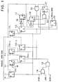
- Fig. 1 shows the configuration of a parallel-serial data converter according to a first embodiment of the present invention.
- a parallel-serial data converter of the present invention comprises latch circuits 11, 13 n-1 to 131 and 23, selectors 12 n-1 to 121, 17, 19 and 21, an OR circuit 14, AND circuits 15, 20 and 22, inverters 16 and 18 as well as a set latch circuit 21.
- the latch circuit 11 processes parallel data having n bits in sign magnitude notation (I1, Vietnamese, I n-2 , I n-1 , and I n ) to latch the data I n serving as the sign bit according to the STORE signal.
- the selector 12 n-1 receives, from n bits of parallel data in sign magnitude notation, the data I n-1 as input A, and receives the ground potential as input B and selects either of them according to the STORE signal.
- the selectors 12 n-2 to 121 have the parallel data I1 to I n-2 as input A and the output from the latch circuits 13 n-1 to 132 as input B and select either of them according to the STORE signal.
- the latch circuits 13 n-1 to 131 receive the outputs from the selectors 12 n-1 to 121.
- the OR circuit 14 takes the logical OR the STORE signal and the LOAD signal and the AND circuit 15 takes the logical AND the output from the OR circuit 14 and the CLOCK signal.
- the above latch circuits 13 n-1 to 131 operate with using the output from the AND circuit 15 as the clock.
- the selector 17 receives the output from the inverter 16 where the output from the latch circuit 131 is reversed as input A and the output from the latch circuit 131 as input B and selects either of them according to the output from the latch circuit 11.
- the selector 19 receives the output of the inverter 18 where the output from the selector 17 is reversed as input A and the output of the selector 17 as input B and selects either of them according to the output from the AND circuit 20.
- the set latch circuit 21 receives the output from the AND circuit 22 which takes the logical AND the output from the AND circuit 20 and the output from the selector 17 as the input D and the STORE signal as a set signal.
- the AND circuit 20 takes the logical AND the output from the latch circuit 11 and the set latch circuit 21.
- the latch circuit 23 receives the output from the selector 19 as the data input and operates with using the output from the AND circuit 15 as the clock so as to output serial data.
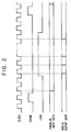
- Fig. 2 is a timing chart of input/output signals related to the operation according to the first embodiment.
- the sign bit I n is latched by the latch circuit 11 according to the STORE signal.
- the remaining parallel data I1, I n-2 and I n-1 are processed differently depending on the STORE signal level. If the STORE signal is at H level, the selectors 121, Vietnamese, 12 n-2 and 12 n-1 select input A, which is in turn latched by the latch circuits 131, Across, 13 n-2 and 13 n-1 respectively according to the output from the AND circuit 15.
- the set latch circuit 21 is set via the STORE signal at H level. If the STORE signal is at L level, the selectors 121, Vietnamese, 12 n-2 , 12 n-1 select input B, with resulting in serial connection of the latch circuits 131 to 13 n-1 . In this case, however, the input to the latch circuit 13 n-1 is the ground potential, or at L level. At the selectors 17 and 19, the output from the latch circuit 11 is at L level, and the output from the AND circuit 20 is also at L level. This means that both selectors select input B.
- the AND circuit 15 outputs the clock signal.
- the latch circuit 23 subsequently outputs serial data in two's compliment notation. The serial data are output one by one from the least significant bit.
- the sign bit I n is at H level.
- the sign bit I n is latched and stored by the latch circuit 11 according to the STORE signal.
- the remaining data I1, ??, I n-2 and I n-1 are processed differently depending on the STORE signal level. If the STORE signal is at H level, the selectors 121, ??, 12 n-2 and 12 n-1 select input A, which is in turn latched by the latch circuits 131, 13 n-2 and 13 n-1 respectively according to the output from the AND circuit 15. At the same time, the set latch circuit 11 is set via the STORE signal.
- the selectors 121, ??, 12 n-2 and 12 n-1 select input B, with resulting in serial connection of the latch circuits 131, ising, 13 n-2 and 13 n-1 .
- the input to the latch circuit 13 n-1 is the ground potential.
- the selector 17 selects input A for output because the output from the latch circuit 11 is at H level.
- the outputs from the latch circuit 131 are reversed before being output from the selector 17. Since the output from the latch circuit 11 is at H level, the output level of the AND circuit 20 depends on the output level of the set latch circuit 21. Note that the set latch circuit 21 is in set status at first with its output level at "H". Therefore, the output level of the AND circuit 20 is at H level at first, which causes the selector 19 to select input A for output.
- the data output from the latch circuit 131 via the CLOCK signal from the AND circuit 15 is reversed twice during the first CLOCK signal (H level) at the selectors 17 and 19 which select input A as described above and as a result output the data to the latch circuit 23 as it is.
- the latch circuit 23 provides "1” if the first output data from the latch circuit 13 1 is “1", and "0" if it is "0".
- a value determined by the AND circuit 22 as the logical product of the set signal selected by the previous cycle CLOCK signal (output from the AND circuit 20) and the previous cycle output from the selector 17 is latched by the set latch circuit 21, output via the AND circuit 20 and sent to the selector terminal S of the selector 19 so that either of input A or B is selected.
- the latch circuit 131 outputs "0" as the first output data and "1" as the second output data, since the set signal selected according to the CLOCK signal of the previous cycle (output from the AND circuit 20) is "1" and the output from the selector 17 of the previous cycle is reversed to be “1", the AND circuit 22 outputs "1" and the AND circuit 20 outputs "1". Therefore, the selector 19 selects input A, which causes the above second output data "1" to be reversed twice and read out as "1".
- the latch circuit 131 If the latch circuit 131 outputs "1" as the first output data and "1" as the second output data, then the set signal selected according to the CLOCK signal of the previous cycle (output from the AND circuit 20) is "1" and the output from the selector 17 of the previous cycle is reversed to be “0", and the AND circuit 22 outputs "0" and the AND circuit 20 outputs "0". Therefore, the selector 19 selects input B and the above second output data '1" is reversed once and read out as "0".
- serial data in two's compliment notation from the latch circuit 23 is output synchronizing with the CLOCK signal.
- the selectors 12 n-1 to 121 and the selectors 17 and 19 should be set to have a delay time exceeding the rise time of the clock signal so as to ensure latching at the latch circuits 13 n-1 to 131 and the latch circuit 23. If the selectors 12 n-1 to 121 and selectors 17 and 19 have a delay time shorter than the rise time of the clock signal, the first rising of the clock signal upon entering of LOAD signal to H level causes the latch circuits 13 n-1 to 131 and the latch circuit 23 to enter "through" status and all of them have the same level as the ground potential (L level).
- the selectors 12 n-1 to 121 and the selectors 17 and 19 have a delay time more than the rise time of the clock signal, then the parallel data latched by the latch circuits 13 n-1 to 131 are subsequently transmitted.
- a converter according to the first embodiment is capable of data conversion without judging whether each data bit in serial output is a sign bit or not.
- Fig. 3 shows the configuration of a parallel-serial data converter according to a second embodiment of the present invention.
- the latch circuits 13 n-1 to 131 and the latch circuit 23 in the first embodiment of Fig. 1 are replaced with the latch circuits 33 n-1 to 331 and 43 comprising two-phase D type flip-flops operating according to the master-slave method.
- master CLOCK (1) and slave CLOCK (2) are provided for CLOCK signals.
- master CLOCK (1) and slave CLOCK (2) are provided.
- the AND circuit 15 which takes the logical AND the output from the OR circuit 14 and master CLOCK (1)
- another AND circuit 35 is added to AND the output from the OR circuit 14 and slave CLOCK (2). Except these points, this embodiment has the same configuration as in Fig. 1.
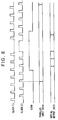
- Fig. 4 is a timing chart of input/output signals in conversion operation according to the second embodiment.
- the second embodiment basically works in the same way as the first embodiment except that parallel data latching and serial data output are synchronized with the slave CLOCK (2).
- adoption of latch circuits using master/slave method eliminates the need of consideration for delay time at the selectors 12 n-1 to 121 to ensure latching operation at the latch circuits as in the first embodiment.
- the third embodiment is a parallel-serial data converter which can cope with absence of the STORE signal.
- Fig. 5 is a block diagram to show the third embodiment. It is supposed here that the parallel data is fixed at least one clock before the LOAD signal and kept invariable while the LOAD signal is at H level. In other words, this is a circuit configuration to continue, even after the parallel data is fixed, to receive the same parallel data.
- a parallel-serial data converter comprises selectors 501, ??, 50 n-2 and 50 n-1 , latch circuits 512, ising, 51 n-2 and 51 n-1 , a latch circuit 511, inverters 53 and 54, a selector 55, an inverter 56, a selector 57, AND circuits 58 and 60, a set latch circuit 59 and a latch circuit 63.
- the selectors 501, ??, 50 n-2 and 50 n-1 receive the data except the sign bit In (I1, ??, I n-2 and I n-1 ) as input A.
- the latch circuits 512, ??, 51 n-2 and 51 n-1 which latch the outputs from the selectors 501, ??, 50 n-2 and 50 n-1 via the CLOCK signal and return them via the LOAD signal reversed at the converter 53 to the corresponding selectors 501, nowadays, 50 n-2 as input B.
- the latch circuit 51, the inverter 54, the selector 55, the inverter 56, the selector 57, the AND circuit 58, the set latch circuit 59 and the AND circuit 60 correspond to the latch circuit 131, the inverter 16, the selector 17, the inverter 18, the selector 19, the AND circuit 20, the set latch circuit 21 and the AND circuit 22 in the first embodiment respectively.
- Fig. 6 is a timing chart of input/output signals
- the operation of the converter according to this embodiment is compared with that in the first embodiment.
- the parallel data except the sign bit In (I1, ??, I n-2 and I n-1 ) are latched according to the STORE signal.
- latching is made according to the CLOCK signal while the LOAD signal is at L level.
- the circuit comprising the latch circuit 51, the inverter 54, the selector 55, the inverter 56, the selector 57, the AND circuits 58 and 60 and the set latch circuit 59 as in the first embodiment operates in the same way as the first embodiment and the description is omitted.
- Fig. 7 is a parallel-serial data converter according to a fourth embodiment of the present invention.
- the latch circuits 51 n-1 to 511 and the latch circuit 53 in the third embodiment are replaced with latch circuits 71 n-1 to 711 and a latch circuit 73 comprising two-phase D type flip-flops operating according to the master/slave method.
- master CLOCK (1) and slave CLOCK (2) are input to the latch circuits.
- Fig. 8 is a timing chart to show the operation in the fourth embodiment. Except that the parallel data latching and the serial data output are synchronized with the slave CLOCK (2), the operation is exactly the same as in the first and the third embodiments.
- exclusive OR circuits and adders required for the number of bits in a conventional converter are replaced with a latch circuit and a set latch circuit, two selectors, two inverters and two AND circuits. This largely reduces the number of circuit elements resulting in a smaller scale circuit.
- the present invention is particularly effective when applied to a converter for a large number of bits.
Landscapes
- Engineering & Computer Science (AREA)
- Theoretical Computer Science (AREA)
- Complex Calculations (AREA)
- Communication Control (AREA)
- Analogue/Digital Conversion (AREA)
- Synchronisation In Digital Transmission Systems (AREA)
Applications Claiming Priority (3)
| Application Number | Priority Date | Filing Date | Title |
|---|---|---|---|
| JP209909/92 | 1992-08-06 | ||
| JP20990992 | 1992-08-06 | ||
| JP4209909A JP2766133B2 (ja) | 1992-08-06 | 1992-08-06 | パラレル・シリアル・データ変換回路 |
Publications (3)
| Publication Number | Publication Date |
|---|---|
| EP0582311A2 true EP0582311A2 (de) | 1994-02-09 |
| EP0582311A3 EP0582311A3 (de) | 1995-03-08 |
| EP0582311B1 EP0582311B1 (de) | 1999-11-03 |
Family
ID=16580664
Family Applications (1)
| Application Number | Title | Priority Date | Filing Date |
|---|---|---|---|
| EP93112655A Expired - Lifetime EP0582311B1 (de) | 1992-08-06 | 1993-08-06 | Parallel-Serien-Umsetzer |
Country Status (4)
| Country | Link |
|---|---|
| US (1) | US5379038A (de) |
| EP (1) | EP0582311B1 (de) |
| JP (1) | JP2766133B2 (de) |
| DE (1) | DE69326923T2 (de) |
Cited By (1)
| Publication number | Priority date | Publication date | Assignee | Title |
|---|---|---|---|---|
| EP0788240A2 (de) * | 1996-01-31 | 1997-08-06 | Nec Corporation | Multiplexer mit einem Schieberegister |
Families Citing this family (5)
| Publication number | Priority date | Publication date | Assignee | Title |
|---|---|---|---|---|
| US5563594A (en) * | 1994-08-31 | 1996-10-08 | Motorola | Circuit and method of timing data transfers |
| US6049236A (en) * | 1997-11-17 | 2000-04-11 | Lucent Technologies Inc. | Divide-by-one or divide-by-two qualified clock driver with glitch-free transitions between operating frequencies |
| US5982309A (en) * | 1998-01-09 | 1999-11-09 | Iowa State University Research Foundation, Inc. | Parallel-to-serial CMOS data converter with a selectable bit width mode D flip-flop M matrix |
| KR100340058B1 (ko) * | 1998-06-27 | 2002-07-18 | 박종섭 | 버스신호전송장치 |
| JP6977883B2 (ja) * | 2018-05-22 | 2021-12-08 | 日本電気株式会社 | 信号処理装置、方法、プログラム |
Citations (3)
| Publication number | Priority date | Publication date | Assignee | Title |
|---|---|---|---|---|
| US3914590A (en) * | 1974-11-04 | 1975-10-21 | Gen Electric | Serial two{3 s complementer |
| US4418418A (en) * | 1981-01-13 | 1983-11-29 | Tokyo Shibaura Denki Kabushiki Kaisha | Parallel-serial converter |
| JPS6156520A (ja) * | 1984-08-27 | 1986-03-22 | Nec Corp | コ−ド変換回路 |
Family Cites Families (5)
| Publication number | Priority date | Publication date | Assignee | Title |
|---|---|---|---|---|
| US3631464A (en) * | 1969-03-21 | 1971-12-28 | Singer General Precision | Digital parallel to serial converter |
| JPS55141823A (en) * | 1979-04-24 | 1980-11-06 | Fujitsu Ltd | Data read-out circuit |
| US4218758A (en) * | 1978-06-30 | 1980-08-19 | International Business Machines Corporation | Parallel-to-serial binary data converter with multiphase and multisubphase control |
| US4377806A (en) * | 1981-05-13 | 1983-03-22 | International Business Machines Corporation | Parallel to serial converter |
| JP2504568B2 (ja) * | 1989-06-20 | 1996-06-05 | 富士通株式会社 | 信号生成回路 |
-
1992
- 1992-08-06 JP JP4209909A patent/JP2766133B2/ja not_active Expired - Fee Related
-
1993
- 1993-08-04 US US08/101,922 patent/US5379038A/en not_active Expired - Fee Related
- 1993-08-06 DE DE69326923T patent/DE69326923T2/de not_active Expired - Fee Related
- 1993-08-06 EP EP93112655A patent/EP0582311B1/de not_active Expired - Lifetime
Patent Citations (3)
| Publication number | Priority date | Publication date | Assignee | Title |
|---|---|---|---|---|
| US3914590A (en) * | 1974-11-04 | 1975-10-21 | Gen Electric | Serial two{3 s complementer |
| US4418418A (en) * | 1981-01-13 | 1983-11-29 | Tokyo Shibaura Denki Kabushiki Kaisha | Parallel-serial converter |
| JPS6156520A (ja) * | 1984-08-27 | 1986-03-22 | Nec Corp | コ−ド変換回路 |
Non-Patent Citations (2)
| Title |
|---|
| COMPUTER DESIGN, vol.18, no.7, July 1979, LITTLETON, US pages 105 - 112 T. V. NGUYEN 'Practical Hardware Solutions for 2's Complement Arithmetic Problems' * |
| PATENT ABSTRACTS OF JAPAN vol. 10, no. 221 (E-424) 2 August 1986 & JP-A-61 056 520 (NEC CORP) 22 March 1986 * |
Cited By (2)
| Publication number | Priority date | Publication date | Assignee | Title |
|---|---|---|---|---|
| EP0788240A2 (de) * | 1996-01-31 | 1997-08-06 | Nec Corporation | Multiplexer mit einem Schieberegister |
| EP0788240A3 (de) * | 1996-01-31 | 1998-09-02 | Nec Corporation | Multiplexer mit einem Schieberegister |
Also Published As
| Publication number | Publication date |
|---|---|
| JPH0661871A (ja) | 1994-03-04 |
| DE69326923D1 (de) | 1999-12-09 |
| US5379038A (en) | 1995-01-03 |
| JP2766133B2 (ja) | 1998-06-18 |
| DE69326923T2 (de) | 2000-06-29 |
| EP0582311A3 (de) | 1995-03-08 |
| EP0582311B1 (de) | 1999-11-03 |
Similar Documents
| Publication | Publication Date | Title |
|---|---|---|
| US4472788A (en) | Shift circuit having a plurality of cascade-connected data selectors | |
| EP0477582B1 (de) | Digitale Frequenzmultiplikation und Datenserialisierungsschaltkreis | |
| US5136292A (en) | Serial data receiving circuit for serial to parallel conversion | |
| US20040222826A1 (en) | Data form converter between serial and parallel | |
| EP0397358A1 (de) | Parallel-Seriell-Umsetzer | |
| US4527148A (en) | Analog-digital converter | |
| US5079548A (en) | Data packing circuit in variable length coder | |
| US20020075173A1 (en) | Parallel in serial out circuit for use in data communication system | |
| EP0404127A2 (de) | Signalgenerator | |
| US4802192A (en) | Circuit for detecting synchronizing code | |
| US4876704A (en) | Logic integrated circuit for scan path system | |
| US5299145A (en) | Adder for reducing carry processing | |
| US5379038A (en) | Parallel-serial data converter | |
| WO1999060702A1 (en) | Low power counters | |
| US5200647A (en) | High-speed signal multiplexing circuit for multiplexing high-speed signals | |
| EP0661820B1 (de) | Parallel-zur-seriell-Datenumsetzungsschaltung | |
| US5761100A (en) | Period generator for semiconductor testing apparatus | |
| US5293165A (en) | 5B6B coding rule inverse conversion circuit for digital transmission | |
| EP0282924B1 (de) | Kodierschaltung mit bipolarer Acht- und Sechsnullfolgensubstitution | |
| US5615141A (en) | Multiplying apparatus | |
| KR100353533B1 (ko) | 딜레이 락 루프 회로 | |
| JP3135990B2 (ja) | パリティ付加回路 | |
| US4811271A (en) | Expandable bi-phase convolving element | |
| US6314156B1 (en) | Space-efficient multi-cycle barrel shifter circuit | |
| JP3145988B2 (ja) | データs/p変換回路 |
Legal Events
| Date | Code | Title | Description |
|---|---|---|---|
| PUAI | Public reference made under article 153(3) epc to a published international application that has entered the european phase |
Free format text: ORIGINAL CODE: 0009012 |
|
| AK | Designated contracting states |
Kind code of ref document: A2 Designated state(s): DE FR GB |
|
| PUAL | Search report despatched |
Free format text: ORIGINAL CODE: 0009013 |
|
| AK | Designated contracting states |
Kind code of ref document: A3 Designated state(s): DE FR GB |
|
| 17P | Request for examination filed |
Effective date: 19950620 |
|
| 17Q | First examination report despatched |
Effective date: 19970515 |
|
| GRAG | Despatch of communication of intention to grant |
Free format text: ORIGINAL CODE: EPIDOS AGRA |
|
| GRAG | Despatch of communication of intention to grant |
Free format text: ORIGINAL CODE: EPIDOS AGRA |
|
| GRAH | Despatch of communication of intention to grant a patent |
Free format text: ORIGINAL CODE: EPIDOS IGRA |
|
| GRAH | Despatch of communication of intention to grant a patent |
Free format text: ORIGINAL CODE: EPIDOS IGRA |
|
| GRAA | (expected) grant |
Free format text: ORIGINAL CODE: 0009210 |
|
| AK | Designated contracting states |
Kind code of ref document: B1 Designated state(s): DE FR GB |
|
| REF | Corresponds to: |
Ref document number: 69326923 Country of ref document: DE Date of ref document: 19991209 |
|
| ET | Fr: translation filed | ||
| PLBE | No opposition filed within time limit |
Free format text: ORIGINAL CODE: 0009261 |
|
| STAA | Information on the status of an ep patent application or granted ep patent |
Free format text: STATUS: NO OPPOSITION FILED WITHIN TIME LIMIT |
|
| 26N | No opposition filed | ||
| REG | Reference to a national code |
Ref country code: GB Ref legal event code: IF02 |
|
| REG | Reference to a national code |
Ref country code: GB Ref legal event code: 732E |
|
| REG | Reference to a national code |
Ref country code: FR Ref legal event code: TP |
|
| PGFP | Annual fee paid to national office [announced via postgrant information from national office to epo] |
Ref country code: GB Payment date: 20050803 Year of fee payment: 13 |
|
| PGFP | Annual fee paid to national office [announced via postgrant information from national office to epo] |
Ref country code: DE Payment date: 20050804 Year of fee payment: 13 |
|
| PGFP | Annual fee paid to national office [announced via postgrant information from national office to epo] |
Ref country code: FR Payment date: 20050809 Year of fee payment: 13 |
|
| PG25 | Lapsed in a contracting state [announced via postgrant information from national office to epo] |
Ref country code: DE Free format text: LAPSE BECAUSE OF NON-PAYMENT OF DUE FEES Effective date: 20070301 |
|
| GBPC | Gb: european patent ceased through non-payment of renewal fee |
Effective date: 20060806 |
|
| REG | Reference to a national code |
Ref country code: FR Ref legal event code: ST Effective date: 20070430 |
|
| PG25 | Lapsed in a contracting state [announced via postgrant information from national office to epo] |
Ref country code: GB Free format text: LAPSE BECAUSE OF NON-PAYMENT OF DUE FEES Effective date: 20060806 |
|
| PG25 | Lapsed in a contracting state [announced via postgrant information from national office to epo] |
Ref country code: FR Free format text: LAPSE BECAUSE OF NON-PAYMENT OF DUE FEES Effective date: 20060831 |