EP0581519A2 - Optisches Wiedergabegerät - Google Patents
Optisches Wiedergabegerät Download PDFInfo
- Publication number
- EP0581519A2 EP0581519A2 EP93305753A EP93305753A EP0581519A2 EP 0581519 A2 EP0581519 A2 EP 0581519A2 EP 93305753 A EP93305753 A EP 93305753A EP 93305753 A EP93305753 A EP 93305753A EP 0581519 A2 EP0581519 A2 EP 0581519A2
- Authority
- EP
- European Patent Office
- Prior art keywords
- light
- optical
- optical disk
- photo detector
- emitting element
- Prior art date
- Legal status (The legal status is an assumption and is not a legal conclusion. Google has not performed a legal analysis and makes no representation as to the accuracy of the status listed.)
- Granted
Links
Images


Classifications
-
- G—PHYSICS
- G11—INFORMATION STORAGE
- G11B—INFORMATION STORAGE BASED ON RELATIVE MOVEMENT BETWEEN RECORD CARRIER AND TRANSDUCER
- G11B7/00—Recording or reproducing by optical means, e.g. recording using a thermal beam of optical radiation by modifying optical properties or the physical structure, reproducing using an optical beam at lower power by sensing optical properties; Record carriers therefor
- G11B7/12—Heads, e.g. forming of the optical beam spot or modulation of the optical beam
- G11B7/135—Means for guiding the beam from the source to the record carrier or from the record carrier to the detector
- G11B7/1353—Diffractive elements, e.g. holograms or gratings
-
- G—PHYSICS
- G11—INFORMATION STORAGE
- G11B—INFORMATION STORAGE BASED ON RELATIVE MOVEMENT BETWEEN RECORD CARRIER AND TRANSDUCER
- G11B7/00—Recording or reproducing by optical means, e.g. recording using a thermal beam of optical radiation by modifying optical properties or the physical structure, reproducing using an optical beam at lower power by sensing optical properties; Record carriers therefor
- G11B7/12—Heads, e.g. forming of the optical beam spot or modulation of the optical beam
- G11B7/123—Integrated head arrangements, e.g. with source and detectors mounted on the same substrate
-
- G—PHYSICS
- G11—INFORMATION STORAGE
- G11B—INFORMATION STORAGE BASED ON RELATIVE MOVEMENT BETWEEN RECORD CARRIER AND TRANSDUCER
- G11B7/00—Recording or reproducing by optical means, e.g. recording using a thermal beam of optical radiation by modifying optical properties or the physical structure, reproducing using an optical beam at lower power by sensing optical properties; Record carriers therefor
- G11B7/12—Heads, e.g. forming of the optical beam spot or modulation of the optical beam
- G11B7/125—Optical beam sources therefor, e.g. laser control circuitry specially adapted for optical storage devices; Modulators, e.g. means for controlling the size or intensity of optical spots or optical traces
- G11B7/126—Circuits, methods or arrangements for laser control or stabilisation
Definitions
- the present invention relates to an optical pick- up apparatus, which is used to record information into an optical disk and to reproduce the recorded information from the same.
- An optical pick-up apparatus associated with an optical disk device utilizes a laser beam for record and reproduction of information.
- a plurality of holographic optical elements have been conventionally used.
- a method of reflecting a laser beam several times in a light guide For instance, the Japanese Unexamined Patent Applications Nos. 146444/1987 and 155529/1989 disclose a long and thin light guide made of transparent substance. In this light guide, a going laser beam is reflected several times and reaches an optical disk passing through a holographic optical element. The optical disk memorizes information on the surface thereof in the form of unit of spots or depressions.
- a returning laser beam reflected at the recording surface of the optical disk is again reflected several times in the light guide but is guided via a different path to an photo detector.
- the Japanese Unexamined Patent Application No. 20737/1988 discloses two holographic optical elements. One converges a going laser beam onto an optical disk and the other converges a returning laser beam reflected at the optical disk to a photo detector.
- Japanese Unexamined Patent Applications Nos. 81335/1990 and 220145/1989 disclose holographic optical elements integrally assembled with objective lenses used for causing diffraction in a returning beam after being reflected at an optical disk.
- Fig. 22 shows an optical pick- up apparatus utilizing a plurality of reflections of a laser beam, as represented by the Japanese Unexamined Patent Applications Nos. 146444/1987 and 155529/1989.
- Fig. 23 shows an optical pick-up apparatus including a pair of holographic optical elements, one holographic optical element converging a going laser beam and the other holographic optical element causing diffraction of a returning laser beam, which is similarto that disclosed in the Japanese Unexamined Patent Application No. 20737/1988.
- Fig. 22 shows an optical pick-up apparatus utilizing a plurality of reflections of a laser beam, as represented by the Japanese Unexamined Patent Applications Nos. 146444/1987 and 155529/1989.
- Fig. 23 shows an optical pick-up apparatus including a pair of holographic optical elements, one holographic optical element converging a going laser beam and the other holographic optical element causing diffraction of a returning laser beam, which is similarto that disclosed in the
- FIG. 24 shows an optical pick-up apparatus using an objective lens on the spherical surface of which a holographic optical element is integrally or directly formed to cause diffraction of a laser beam, the same type as that disclosed by the Japanese Unexamined PatentApplica- tion No. 81335/1990.
- Fig. 25 shows an optical pick-up apparatus using a complex objective lens whose body is split into two by a plane normal to an axis thereof. A holographic optical element for diffraction is sandwiched therebetween, as is disclosed in the Japanese Unexamined Patent Application No. 220145/1989.
- a reference numeral 501 represents a laser diode emitting a laser beam.
- a reference numeral 504 represents a holographic optical element converging the laser beam emitted from the laser diode 501 onto an optical disk 503 whose surface are formed with the unit of spots memorizing information being sensed by the laser beam.
- a reference numeral 502 represents a light guide which is made of a transparent substance such as fused silica and causes a laser beam to reflect repeatedly at inside, upper and lower, surfaces thereof.
- a reference numeral 505 represents a holographic optical element of reflection type which reflects a returning laser beam having once reached and been reflected at the surface of the optical disk 503 and also diffracts this returning laser beam toward a photo detector 506.
- a reference numeral 507 represents a holographic optical element of transmission type which transmits a returning laser beam having been reflected at the surface of the optical disk 503 and also diffracts this returning laser beam toward the photo detector 506.
- the laser diode 501, optical disk 503, holographic optical element 504, and photo detector 506 are substantially the same as those explained with reference to Fig. 18.
- a reference numeral 508 represents an objective lens converging a laser beam emitted from the laser diode 501 onto the optical disk 503.
- a reference numeral 509 represents a holographic optical element of transmission type which transmits a returning laser beam having been reflected at the surface of the optical disk 503 and also diffracts this returning laser beam toward the photo detector 506.
- the laser diode 501, the optical disk 503, and the photo detector 506 are substantially the same as those explained with reference to Fig. 22.
- a reference numeral 510 represents a complex objective lens whose body is split by a plane normal to an axis thereof into two, upper and lower, half bodies.
- This complex objective lens 510 converges a laser beam emitted from the laserdiode 501 onto the surface of the optical disk 503.
- a reference numeral 511 represents a holographic optical element of transmission type which transmits a returning laser beam having been reflected at the surface of the optical disk 503 and also diffracts this returning laser beam toward the photo detector 506.
- This holographic optical element 511 is sandwiched by and integrally fabricated with the paired half bodies of the complex objective lens 510.
- the laser diode 501, the optical disk 503, and the photo detector 506 are substantially the same as those explained with reference to Fig. 22.
- a laser beam is emitted from the laser diode 501 and, then, reflected plural times at inside, upper and lower, surfaces of the light guide 502 so as to reach the holographic optical element 504.
- the holographic optical element 504 then converges the laser beam thus guided through the light guide 502 onto the surface of the optical disk 503.
- the laser beam is reflected at the surface, i.e. a recording surface, of the optical disk 503 and returns as a beam including information read out from the optical disk 503.
- the returning beam passes through the holographic optical element 504 again and, in turn, reaches the holographic optical element 505 of reflection type.
- This holographic optical element 505 not only reflects the returning laser beam but diffracts it toward the photo detector 506.
- the photo detector 506 receives the returning laser beam and detects focusing error and tracking error, as well as the read-out information.
- the optical pick-up apparatus shown in Figs. 23, 24, and 25 operate in the same manner as that shown in Fig. 22.
- a laser beam emitted from the laser diode 501 is converged onto the recording surface of the optical disk 503 passing through the holographic optical element 504, the objective lens 508, or the split-type complex objective lens 510, respectively.
- the returning beam comprising information read out from the optical disk 503 passes through the holographic optical elements 507, 509, or 511 respectively and is diffracted toward the photo detector 506.
- the photo detector 506 receives the returning laser beam and detects focusing error and tracking error, as well as the read-out information.
- the conversing arrangement and the diffracting arrangement are independent from each other.
- the conversing arrangement conversing a laser beam is constituted by the holographic optical element 504, the objective lens 508, or the split-type objective lens 510.
- the diffracting arrangement diffracting the laser beam is constituted by the reflection-type holographic optical element 505 or the transmission-type holographic optical element 507, 509, 511. These conversing arrangement and the diffracting arrangement are independently mounted on the light guide 502 or installed into a casing.
- the constructional requirement of forming the transmission-type holographic optical element 509 directly on the objective lens 508 further increases the complicateness. This will be easily understood from the spherical surface of the objective lens 508 which makes the formation of the transmission-type holographic optical element 509 thereon difficult. Still further, in case of the optical pick-up apparatus shown in Fig. 25, the structure of sandwiching the transmission-type holographic optical lens 511 between the split half bodies of the complex objective lenses 510 is not only time-consuming in its assembling but tends to cause unacceptable deterioration in lens property.
- the present invention has a purpose, in view of above-described problems or disadvantages encountered in the prior art, to provide an optical pick-up apparatus capable of realizing both the conversion of a laser beam to the optical disk and/or the photo detector and the differentiation of going and returning laser beam paths, by use of only one holographic optical element, thereby providing cheaper optical pick-up apparatus.
- the present invention provides not more than one compound holographic optical element on an optical path starting from a semiconductor laser chip and arriving at a photo detector via an optical disk.
- a hologram pattern of this compound holographic optical element is the superposition of a first hologram pattern, converging a laser beam emitted from the semiconductor laser chip onto the optical disk, and a second hologram pattern, diffracting the laser beam reflected at the optical disk toward the photo detector and changing it into a focusing beam.
- This single holographic optical element not only realizes the convergence of the laser beam onto the optical disk and/or the photo detector and the differentiation of going and returning optical paths but reduces the size and production cost of the optical pick-up apparatus.
- another aspect of the present invention provides a single holographic optical element having at least one hologram pattern.
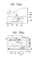
- Fig. 1 (a) is a schematic view showing an optical pick-up apparatus in accordance with a first embodiment of the present invention.
- Fig. 1(b) is a view showing a hologram pattern of the first embodiment, which is constituted by superposing a first hologram pattern and a second hologram pattern.
- Fig. 1 (c) is a view solely showing the first hologram pattern, and
- Fig. 1(d) is a view solely showing the second hologram pattern.
- FIG. 1(a) a transparent glass substance 1 gas a bottom surface 1 a, at a center of which a semiconductor laser chip 2 is mounted securely.
- This semiconductor laser chip 2 emits a laser beam 3, which diffuses or diverges in the glass substance 1 and reaches a compound holographic optical element 4 formed on a top surface 1 b of the glass substance 1.
- the compound holographic optical element 4 is depicted two hologram patterns superposed as shown in Fig. 1(b).
- One hologram pattern has a concentric circles pattern, in which a center of these concentric circles positions at a center of the hologram pattern and a pitch between adjacent two circles becomes small as it goes outside as shown in Fig. 1 (c).
- This hologram pattern serves as a first hologram pattern 4a capable of focusing the diffused laser beam 3 onto an information recording layer 7a of an optical disk 7 as a spot 8.
- the laser beam 3 emitted from the semiconductor laser chip 2 passes through the glass substance 1, diffusing symmetrically about an axis of the glass substance 1 and, in turn, passes through the compound holographic optical element 4 disposed normal to the axis of the glass substance 1. Then, the laser means 3 is converged along the axis of the glass substance 1 onto the recording layer 7a of the optical disk 7.
- the other hologram pattern has eccentric circles pattern, whose center is offset left in the drawing, which is different from that of the above-described first hologram pattern.
- This hologram pattern serves as a second hologram pattern 4b capable of converting the laser beam, being reflected at the recording layer 7a of the optical disk 7 and returning the same optical path 6 as the going laser beam, into a focusing beam 10, and also capable of diffracting this focusing beam 10 toward a quadrant photo detector 9 and conversing it onto the same.
- This second hologram pattern 4b is capable of causing astigmatic aberration as well as conversing the focusing beam 10.
- this second hologram pattern 4b allows the photo detector 9 to detect focusing error on the basis of the received beam 10. This is well known to those skilled in the art as the astigmatic method.
- the compound holographic optical element 4 whose hologram pattern is the superposition of these first and second hologram patterns 4a and 4b, can be fabricated through various ways such as printing and the 2P (Photo Polymerization) method.
- This 2P method utilizes a resin hardenable through irradiation of ultraviolet ray to transfer the matrix configuration thereon.
- Fig. 2 is a view illustrating change of the focusing beam 10 irradiated onto and sensed by the photo detector 9, the focusing beam 10 passing through the second hologram pattern 4b.
- the second hologram pattern 4b is designed so as to satisfy the requirement of a focusing error signal (F.E) described below.
- the quadrant photo sensor 9 is divided into four segments 9a, 9b, 9c, and 9d. If assumed that l(9a), l(9b), l(9c), and 1(9d) represent output currents detected by these four segments 9a, 9b, 9c, and 9d, respectively, the focusing error signal (F.E.) is defined by the following equation (1).
- a differential amplifier 16a and two operational amplifiers 16b, 16c constitute the signal processing circuit associated with the photo detector 9, so that signals from the photo detector 9 are processed in accordance with above equation (1).
- the differential amplifier 16a serving as an output component of the signal processing circuit for the photo detector 9, generates an output of "0" in this case.
- the present invention requires no more than one holographic optical element, i.e. the compound holographic optical element4, by which the present invention enables the optical pick-up apparatus to converge a laser beam onto the optical disk and/or the photo detector, differentiate the going and returning optical paths, and detecting the focusing error. Therefore, fabrication of the optical pick-up apparatus will be widely simplified compared with the prior art optical pick-up apparatus because positional adjustment of a plurality of holographic optical elements is no more required. As no additional holographic element is necessary, the optical path can be further shortened. This will be helpful to reduce the size of the optical pick-up apparatus.
- FIG. 3(a) is a schematic view showing an optical pick-up apparatus in accordance with the second embodiment of the present invention.
- first photo detector 11 and second photo detector 12 are integrally formed on an upper surface of a sensor substrate 13, so that their light receiving (or photo sensing) planes face upward.
- a semiconductor laser chip 14 At an opposite side of the upper surface of the sensor substrate 13 there is provided a semiconductor laser chip 14. This semiconductor laser chip 14 is parallel to the upper surface of the sensor substrate 13. An axis of the laser beam emitted from a light emitting surface of the semiconductor laser chip 14 is therefore aligned parallel to the upper surface of the sensor substrate 13.
- a reflection prism 15 Adjacent to the semiconductor laser chip 14 on the upper surface of the sensor substrate 13, a reflection prism 15 is located. A positional relationship between this reflection prism 15 and the semiconductor laser chip 14 is adjusted in such a manner that the reflection surface of the reflection prism 15 confronts with the light emitting surface of the semiconductor laser chip 14 so that a laser beam reflected at the reflection surface of the reflection prism 15 goes upward.
- Fig. 3(b) is an enlarged view showing the semiconductor laser chip 14 and the reflection prism 15 shown in Fig. 3(a).
- the reflection prism 15 has a cross section of a trapezoidal shape.
- the reflection surface 15a of the reflection prism 15 is coated by a semi-transmission type film which transmits a part of the laser beam emitted from the semiconductor laser chip 14 into an inside of the reflection prism 15 without being reflected by the reflection surface 15a.
- This arrangement of the monitor sensor 49 with associated reflection prism 15 is unique and advantageous compared with the conventional ones. Because, this kind of monitor sensor has been conventionally located behind the semiconductor laser chip 14, in order to sense a laser beam emitted from a rear surface 14a of the semiconductor laser chip 14. The behind side of the semiconductor laser chip 14 is, however, normally located other photo detectors, e.g. the first and second photo detectors 11 and 12. Therefore, nevertheless its intention, the laser beam emitted toward the monitor sensor tends to cause stray light to these other photo detectors.
- the present invention enables the reflection prism 15 to partly transmit the laser beam toward the monitor sensor 49 disposed beneath the reflection prism 15.
- the present invention no longer emits the laser means from the rear surface 14a of the semiconductor laser chip 14 and therefore no stray light disturb other photo detectors located behind the semiconductor laser chip 14.
- the laser beam having been emitted from the semiconductor laser chip 14, is partly reflected at the reflection surface 15a of the reflection prism 15 toward a light guide 18.
- the light guide 18 is spaced from the semiconductor laser chip 14 and photo detectors 11, 12.
- the light guide 18 has an incident window 17 on its second, i.e. lower, surface 18b.
- the present invention can ensure the accurate setting because of the previously described parallel mounting structure of the semiconductor laser chip 14 with respect to the upper surface of the sensor substrate 13. This parallel mounting structure is also advantageous in facilitating wiring arrangement and heat radiation.
- the light guide 18 has a first, i.e. an upper, surface 18a, disposed in parallel with the second surface 18a.
- the first surface 18a confronts with an optical disk 26 located above the light guide 18.
- a first reflection portion 21 which reflects the laser beam 19 and changes it into the laser beam 20 proceeding to the second surface 18b.
- second reflection portion 23 which reflects the laser beam 20 and changes it into the laser beam 22 proceeding to the first surface 18a.
- the laser beam, entered from the incident window 17, is reflected two times in the light guide 18 by the first and second reflection portions 21, 23 and, in turn, reaches a compound holographic optical element 24 formed in the vicinity of the first reflection portion 21 on the first surface 18a.
- the laser beam 22 enters the compound holographic optical element 24 with the predetermined incident angle
- the light quantity distributions of this laser beam 22 is normally elliptic formation.
- the laser beam normally has a polarization surface in a minor axis direction of its elliptic irradiation beam, it will be preferable to mount the semiconductor laser chip 14 to coincide the optical axis plane and the polarization plane.
- Figs. 4(a) to 4(c) are views illustrating the compound holographic optical element 24.
- This compound holographic optical element 24, shown in Fig. 4(a) is made by superposing a first hologram pattern 24a shown in Fig. 4(b) and a second hologram pattern 24b shown in Fig. 4(c).
- the laser beam 22, entered into the compound holographic optical element 24 with the predetermined incident angle, is converted into a focusing beam 25 therethrough. Subsequently, this focusing beam 25 converges onto an information recording surface 26a of an optical disk 26 as a spot 27.
- the second hologram pattern 24b of the compound holographic optical element 24 converts thus arriving laser beam into a diffracted focusing beam 28.
- the light guide 18 has a semi-transmission type window 29 on the second surface 18b thereof. This semi-transmission type window 29 transmits approximately 50% of the diffracted focusing beam 28 and reflects the remainder, i.e. approximately 50%. With this function of the semi-transmission type window 29, the diffracted focusing beam 28 is split into two. One is a semi-transmission beam 30 reaching the first photo detector 11, and the other is a reflection beam 31 proceeding to the first surface 18a in the light guide 18.
- a reflection film 33 which reflects the reflection beam 31 and changes it into the reflection beam 32 proceeding to the second surface 18b.
- a transmission type window 34 which guides all the reflection beam 32 to the second photo detector 12.
- the diffracted focusing beam 28 has its focal point 35 which is designed to position on an optical path between the semi-transmission window 29 and the second photo detector 12.
- a reference numeral 37 represents a package which is made of non-conductive material such as resin and ceramics.
- a closed space surrounded or sealed by the light guide 18 and the package 37 is normally filled with inert gas such as nitrogen gas. It is also possible to fill this closed space with transparent resin etc.
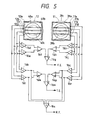
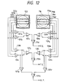
- the first photo detector 11 is divided into four, 11a, 11b, 11 c, and 11d, segments.
- the second photo detector 12 is divided into four, 12a, 12b, 12c, and 12d, segments.
- I(lla), I(llb), 1(11c), 1(11d) and 1(12a), 1(12b), 1(12c), 1(12d) represent output currents detected by these four segments 11a, 11b, 11c, 11d, and 12a, 12b, 12c, 12d, respectively.
- these output currents are processed through the signal processing circuit consisting of numerous operational and differential amplifiers 16d, 16e, 16f, 16g, 16h, 16i, 16j, 16k, 161, 16m, 16n, 16p, 16q, 16r, and 16s.
- This signal processing circuit is designed to fulfill the following equations (5), (6), and (7) so as to obtain the focusing error signal (F.E.), tracking error signal (T.E.), and recording signal (R.F.).
- F.E. focusing error signal
- T.E. tracking error signal
- R.F. recording signal
- the differential amplifier 16g serving as an focusing error signal output component in the signal processing circuit, generates an output of "0" in this case.
- the focusing error detection can be carried out.
- Such a method of detecting the focusing error is known as the spot-size-detection method.
- the tracking error can be detected by the push-pull method.
- this embodiment provides a very simplified construction because no complicated patten normally required for generating the astigmatic aberration is no more required in this embodiment.
- the role of the second hologram pattern 24b of the compound holographic optical element 24 is only converging the beam; therefore the second hologram pattern 24b can be simplified. All thing necessary to effect the advantage of this embodiment is to design the focal point 35 of the diffracted focusing beam 28 such that it resides on the optical path between the semi-transmission type window 29 and the second photo detector 12.
- Figs. 6(a), 6(b), 7(a) and 7(b) show unique constitutions which can more simply realize a focusing error detection compared with the spot-size-detection method.
- a layer of a semi-transmission type film 48 is coated directly on the second surface 18b of the light guide 18.
- both a diffusion film 41 and a light shield film 42 are coated.
- the diffusion film 41 has a ring shape, as shown in Fig. 6(b), so as to surround the semi-transmission window 29.
- the semi-transmission beam residing in a range from d to H is diffused by the diffusion film 41 so as not give adverse effect to the reflection beam 31.
- the diffusion film 41 can be replaced by an absorption film which is capable of absorbing the laser beam.
- the semi-transmission beam 30, having passed through the window 29 of a diameter d, reaches a first photo detector 46.
- Fig. 7(a) shows a reflection beam 32 entering a second photo detector47.
- a light shield film 44 is coated directly on the second surface 18b of the light guide 18, so as to form a transmission window43 having a diameter smaller than that of the reflection beam 32. It will be preferable that this light shield film 44 is continuously coated together with the light shield film 42 of Fig. 6(a).
- Fig. 7(b) shows largeness of the diameter of the reflection beam 32 in contrast with that of the transmission window43. Only a transmission beam 45, having passed the transmission window 43, reaches a second photo detector 47.
- These first and second photo detectors 46 and 47 correspond to the first and second photo detectors 11 and 12 shown in Fig. 3(a); therefore positions at which these photo detectors 46, 47 are located are substantially the same as those of the detectors 11, 12.
- the focal point 35 of the diffracted focusing beam 28 needs to be designed to reside on an optical path between the semi-transmission window 29 and the transmission window 43.
- the first and second photo detectors 46 and 47 are not necessary to be divided into several segments in the same manner as the first and second photo detectors 11 and 12 of Fig. 5. If the first and second photo detectors 46 and 47 have wide light receiving areas sufficient for receiving the semi-transmission beam 30 and the transmission beam 45, an output difference between these first and second photo detectors 46, 47 can be used as the focusing error signal.
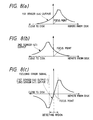
- Figs. 8(a), 8(b), and 8(c) show an output signal of the first photo detector 46, an output signal of the second photo detector47, and focusing error signal obtained by subtracting the output of the second photo detector 47 from the output of the first photo detector 46, respectively.
- this focusing error detecting system As multi-division photo detectors, shown in Fig. 5, are not required in this focusing error detecting system, fine adjustment between the position of the first 46 and/or second 47 photo detectors and the irradiation shape of the laser beam is no more required. Therefore, this focusing error detecting system is superior in productivity and durability.
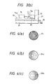
- Fig. 9(a) is a plane view of an optical pick- up apparatus in accordance with the third embodiment of the present invention
- Fig. 9(b) is a sectional view showing the optical pick-up apparatus in accordance with the third embodiment, taken along a line X-X of Fig. 9(a).
- a semiconductor laser chip 102 is mounted in parallel with and on a sensor substrate 101.
- a laser beam 103, emitted horizontally from the semiconductor laser chip 102 reaches a reflection prism 104 mounted on the sensor substrate 101.
- the constitution of this reflection prism 104 and its vicinity is the same as the reflection prism 15 of the second embodiment and, therefore, will no more be explained in detail.
- This reflection prism 104 being trapezoidal shape, has a reflection surface confronting with the light emitting surface of the semiconductor laser chip 102.
- the laser beam having reached the reflection prism 104, is reflected at the reflection surface and enters as a diffusing or diverging beam 107 into the inside of a transparent light guide 105 through an incident window 106 formed on a second surface 105b thereof.
- the light guide 105 is spaced from the semiconductor laser chip 104 and photo detectors 116, 122 later described.
- the light guide 105 has a first surface 105a, disposed in parallel with the second surface 105b.
- On the first surface 105a there is provided a compound holographic optical element 108.
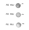
- the compound holographic optical element 108 has a compound hologram pattern shown in Fig. 10(a), which is the superposition of two hologram patterns shown in Figs. 10 (b) and 10(c).
- One hologram pattern shown in Fig. 10(b), has a concentric circles pattern, in which a center of these concentric circles positions at a center of the hologram pattern and a pitch between adjacent two circles becomes small as it goes outside as shown in the drawing.
- This hologram pattern serves as a first hologram pattern 108a capable of focusing the diffused laser beam 107 onto an information recording layer 109a of an optical disk 109 as a spot 110 of a focusing beam 111.
- the laser beam 103 emitted from the semiconductor laser chip 102 passes through the transparent light guide 105, diffusing symmetrically about an axis normal to the first and second surfaces 105a, 105b thereof and, in turn, passes through the compound holographic optical element 108 disposed on the first surface 105a. Then, the laser means is converged along the axis normal to the first surface 105a of the light guide 105 onto the information recording layer 109a of the optical disk 109.
- the other hologram pattern shown in Fig. 10(c), has eccentric circles pattern, whose center is offset lower and left in the drawing, which is different from that of the above-described first hologram pattern.
- This hologram pattern serves as a second hologram pattern 108b capable of converting the laser beam, being reflected at the information recording layer 109a of the optical disk 109 and returning the same optical path as the going laser beam, into a returning focusing beam 112, and also capable of diffracting this returning focusing beam 112 toward the sensor substrate 101 with a predetermined incident angle.
- the second surface 105b of the light guide 105 is formed with a polarized beam splitter 113.
- the polarized beam splitter 113 includes a polarized beam splitting film coated thereon, which can transmits P-polarized component and reflects S-polarized component.
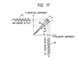
- an arrow shown in Fig. 9(a) represents a linearly polarized beam 114, which expresses the polarization state of the diffusion beam 107 entered into the compound holographic optical element 108.
- the second hologram pattern 108b is designed in such a manner that the diffracted direction of the returning focusing beam 112 is inclined 45° with respect to the polarization direction of the linearly polarized beam 114. Accordingly, the diffracted returning focusing beam 112 includes both P-polarized component and S-polarized component evenly, i.e. at a ratio of approximately 50 : 50.
- This transmission beam 115 is received by a first photo detector 116 provided on an upper surface of the sensor substrate 101.
- the reflection beam 119 goes through a transmission window 120 formed on the second surface 105b and, subsequently, becomes a transmission beam 121.
- This transmission beam 121 is received by a second photo detector 122.
- the compound holographic optical element 108 and others are designed to let a focal point 123 of the diffracted returning focusing beam 112 reside on an optical path between the polarized beam splitter 113 and the second photo detector 122.
- an arrow a denotes a polarization direction of the linearly polarized beam 114 entering the compound holographic optical element 108.
- the compound holographic optical element 108 gives no affection to the polarization surface. Therefore, the diffracted returning focusing beam 112, i.e. the reflection beam of the linearly polarized beam 114, has the same polarization direction as the linearly polarized beam 114 as long as the information recording layer 109a of the optical disk 109 stores no information recorded.
- the information recording layer 109a is not magnetized when it stores no information recorded.
- the compound holographic optical element 108 is designed such that the diffraction direction of the returning focusing beam 112, having such a polarization direction, is inclined 45° with respect to the polarization direction of the linearly polarized beam 114.
- the diffracted returning focusing beam 112 enters at 45°, as shown in Fig. 11, with respect to the polarized beam splitter 113 which transmits almost 100% of the P-polarized component and reflects almost 100% of the S-polarized component.
- the linearly polarized beam 114 is reflected at a magnetized information pit on the optical disk 109, its rotational direction is varied in a range of ⁇ k depending on polarity and strength of the magnetization. (Kerr effect)
- An arrow b denotes a polarization direction of the linearly polarized beam when the linearly polarized beam 114 rotates 8 k from the state of the arrow a.
- An arrow c denotes a polarization direction of the linearly polarized beam when the linearly polarized beam 114 rotates -8 k from the state of the arrow a.
- the P-polarized component to be detected by the first photo detector 116 is obtained as a signal 126 and also the S-polarized component to be detected by the second photo detector 122 is obtained as a signal 127.
- These signals 126 and 127 has a mutual phase difference of 180°, therefore a recording signal component is doubled by performing a differential amplification based on these two signals. Noises having the same phase component are mutually canceled; thus better S/N ratio is obtained.
- the recording signal (R.F.) is obtained from signals of the first and second photo detectors 116 , 122.
- Numerous operational and differential amplifiers 131a, 131b, 131c, 131d, 131e, 131f, 131g,131h,131i,131j,131k,131l,131m,131n,131p, 131q, and 131r are associated to fulfill the following equations (12) (13) and (14) so as to obtain the focusing error signal (F.E.), tracking error signal (T.E.), and recording signal (R.F.).
- F.E. focusing error signal
- T.E. tracking error signal
- R.F. recording signal
- T.E. [ ⁇ I(116a) + I(116b) ⁇ - ⁇ 1(116c) + I(116d) ⁇ ] - [ ⁇ I(122a) + I(122b) ⁇ - ⁇ I(122c) + I(122d) ⁇ ] (13) R.F.
- the inclined angle can be any of 45°, 135°, 225°, and 315°.
- the present invention requires no more than one holographic optical element, i.e. the compound holographic optical element 108, whose hologram pattern is the superposition of the first hologram pattern 108a and the second hologram pattern 108b.
- the present invention enables the optical pick-up apparatus to converge a laser beam onto the optical disk and/or the photo detector, differentiate the going and returning optical paths, and detecting the focusing error.
- fabrication of the optical pick-up apparatus will be widely simplified compared with the prior art optical pick-up apparatus because positional adjustment of a plurality of holographic optical elements is no more required. As no additional holographic element is necessary, the optical path can be further shortened. This will be helpful to reduce the size of the optical pick-up apparatus.
- the second hologram pattern 108b of the compound holographic optical element 108 functions to diffract the reflection beam returning from the optical disk 109 with respect to the polarization direction of the linearly polarized beam fed from the semiconductor laser chip 102 at a predetermined angle of (2n+1) 7 t/4 (n: integer).
- the present invention makes it possible to provide the polarized beam splitter 113 with the diffracted returning focusing beam 112 including both P-polarized component and S-polarized component evenly, i.e. at a ratio of approximately 50: 50.
- Approximately half of the diffracted returning focusing beam 112 transmits the polarized beam splitter 113.
- the transmission beam 115 is received by the first photo detector 116.
- the diffracted returning focusing beam 112 can be split evenly for the first and second photo detectors 116 and 122.
- the compound holographic optical element 108 and polarized beam splitter 113 are very easy because they are patterned or formed on a flat, i.e. the first 105a or second 105b, surface of the light guide 105.
- a flat i.e. the first 105a or second 105b, surface of the light guide 105.
- Fig. 13(a) is a plane view of an optical pick-up apparatus in accordance with the fourth embodiment of the present invention
- Fig. 13(b) is a sectional view showing the optical pick-up apparatus in accordance with the fourth embodiment, taken along a line X-X of Fig. 13(a).
- a semiconductor laser chip 202 is mounted in parallel with and on a sensor substrate 201.
- a laser beam 203, emitted horizontally from the semiconductor laser chip 202 reaches a reflection prism 204 mounted on the sensor substrate 201.
- the constitution of this reflection prism 204 and its vicinity is the same as the reflection prism 15 of the second embodimentand, therefore, will no more be explained in detail.
- This reflection prism 204 being trapezoidal shape, has a reflection surface confronting with the light emitting surface of the semiconductor laser chip 202.
- the laser beam having reached the reflection prism 204, is reflected at the reflection surface and enters obliquely as a diffusing or diverging beam 207 into the inside of a transparent light guide 205 through an incident window 206 formed on a second, i.e. a lower, surface 205b thereof.
- the light guide 205 is spaced from the semiconductor laser chip 202 and photo detectors 216, 222 later described.
- the light guide 205 has a first, i.e. an upper, surface 205a, disposed in parallel with the second surface 205a.
- the first surface 205a confronts with an optical disk 209 located above the light guide 205.
- On the first surface 205a there is provided a first reflection portion 246, which reflects the diffusion beam 207 and changes it into the reflection beam 247 proceeding toward the second surface 205b.
- On the second surface 205b there is provided a second reflection portion 248, which reflects the reflection beam 247 and changes it into the reflection beam 249 proceeding toward the first surface 205a.
- the laser beam, entered from the incident window 206, is reflected two times in the light guide 205 by the first and second reflection portions 246, 248 and, in turn, reaches a compound holographic optical element 208 formed in the vicinity of the first reflection portion 246 on the first surface 205a.
- the polarization state of the laser beam is normally changed upon each reflection.
- the laser beam entered as a linearly polarized beam, may be changed into an elliptic polarized beam after the reflection.
- a phase difference control film which is capable of controlling the phase difference between the first and second reflection portions 246, 248.
- This phase difference control film is, for example, constituted as follows.
- an optical film thickness is expressed by nd, wherein d represents a thickness of the film and n represents a refraction factor.
- An incident angle of a light is 18.35° with respect to the normal of a plane.
- the construction of the phase difference control film is given as a lamination layer consisting of air L-layer (L-layer - H-layer)1
- a meaning of the expression (L-Iayer. H-layer)11 is that a combined layer of (L-layer - H-layer) is repeatedly laminated as much as 11 times.
- the compound holographic optical element 208 has a compound hologram pattern shown in Fig. 14(a), which is the superposition of two hologram patterns shown in Figs. 14 (b) and 14(c).
- One hologram pattern, shown in Fig. 14(b) has eccentric circles pattern, in which a center of these concentric circles positions right of the hologram pattern as shown in the drawing.
- This hologram pattern serves as a first hologram pattern 208a capable of focusing the diffused laser beam 249 onto an information recording layer 209a of the optical disk 209 as a spot 210 of a focusing beam 211.
- the laser beam 203 emitted from the semiconductor laser chip 202 passes through the transparent light guide 205, diffusing obliquely with respect to the first and second surfaces 205a, 205b thereof and, in turn, passes through the compound holographic optical element 208 disposed on the first surface 205a. Then, the laser beam is converged along the axis normal to the first surface 205a of the light guide 205 onto the information recording layer 209a of the optical disk 209.
- the other hologram pattern shown in Fig. 14(c), has eccentric circles pattern, whose center is offset upper and left in the drawing, which is different from that of the above-described first hologram pattern.
- This hologram pattern serves as a second hologram pattern 208b capable of converting the laser beam, being reflected at the spot 210 and returning the same optical path as the going laser beam, into a returning focusing beam 212, and also capable of diffracting this returning focusing beam 212 toward the second surface 205b with a predetermined incident angle.
- the second surface 205b of the light guide 205 is formed with a polarized beam splitter 213.
- the polarized beam splitter 213 includes a polarized beam splitting film coated thereon, which can transmits P-polarized component and reflects S-polarized component of the returning focusing beam 212.
- an arrow shown in Fig. 13(a) represents a linearly polarized beam 214, which expresses the polarization state of the reflection beam 249 entered into the compound holographic optical element 208.
- the second hologram pattern 208b is designed in such a manner that the diffracted direction of the returning focusing beam 212 is inclined 135° with respect to the polarization direction of the linearly polarized beam 214. Accordingly, the diffracted returning focusing beam 212 includes both P-polarized component and S-polarized component evenly, i.e. at a ratio of approximately 50 : 50.
- This transmission beam 215 is received by a first photo detector 216 provided on an upper surface of the sensor substrate 201.
- the reflection beam 219 goes through a transmission window 220 formed on the second surface 205b and, subsequently, becomes a transmission beam 221.
- This transmission beam 221 is received by a second photo detector 222.
- the compound holographic optical element 208 and others are designed to let a focal point 223 of the diffracted returning focusing beam 212 reside on an optical path between the polarized beam splitter 213 and the second photo detector 222.
- the present invention utilizes the reflections occurring inside the optical guide 205 to guide the laser beam 203 emitted from the semiconductor laser chip 202 to the compound holographic optical element 208.
- the optical pickup apparatus can be made small in size.
- the phase difference control film, provided on the reflection surface surely prevents the linearly polarized beam from being changed into the elliptic polarized beam upon the reflection.
- the inclined angle can be any of45°, 135°, 225°, and 315°, i.e. an angle of (2n+1) ⁇ /4 (n: integer).
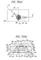
- Fig. 15(a) is a plane view of an optical pick-up apparatus in accordance with the fifth embodiment of the present invention
- Fig. 15(b) is a sectional view showing the optical pick-up apparatus in accordance with the fifth embodiment, taken along a line X-X of Fig. 15(a).
- a semiconductor laser chip 302 is mounted in parallel with and on a sensor substrate 301.
- a laser beam 303 emitted horizontally from the semiconductor laser chip 302, reaches a reflection prism 304 mounted on the sensor substrate 301.
- the constitution of this reflection prism 304 and its vicinity is the same as the reflection prism 15 of the second embodiment and, therefore, will no more be explained in detail.
- This reflection prism 304 being trapezoidal shape, has a reflection surface confronting with the light emitting surface of the semiconductor laser chip 302.
- the laser beam having reached the reflection prism 304, is reflected at the reflection surface and enters obliquely as a diffusing or diverging beam 307 into the inside of a transparent light guide 305 through an incident window 306 formed on a second, i.e. a lower, surface 305b thereof.
- the light guide 305 is spaced from the semiconductor laser chip 302 and photo detectors 316, 322 later described.
- the light guide 305 has a first, i.e. an upper, surface 305a, disposed in parallel with the second surface 305a.
- the first surface 305a confronts with an optical disk 309 located above the light guide 305.
- On the first surface 305a there is provided a going-path reflection portion 346, which reflects the diffusion beam 307 and changes it into the reflection beam 347 proceeding toward the second surface 305b.
- a going-path polarized beam splitter 348 which includes a polarized beam splitting film capable of transmitting P-polarized component and reflecting S-polarized component.
- the laser beam having been reflected by the going-path polarized beam splitter 348, proceeds toward the first surface 305a as a reflection beam 349.
- the laser beam, entered from the incident window 306, is reflected two times in the lightguide 305 by the going-path reflection portion 346 and the going-path polarized beam splitter 348 and, in turn, reaches a compound holographic optical element 308 formed in the vicinity of the going-path reflection portion 346 on the first surface 305a.
- the polarized beam splitting film is used in the going-path polarized beam splitter 348.
- the polarization state of the laser beam is normally changed upon reflection.
- the laser beam entered as a linearly polarized beam, may be changed into an elliptic polarized beam after the reflection.
- it is mandatory to detect a slight Kerr rotation angle caused by the linearly polarized beam irradiated onto the optical disk 309. Hence, it is very important to accurately keep the state of the linearly polarized beam until it reaches the optical disk 309.
- the above-described fourth embodiment adopts the phase difference control film which is capable of controlling the phase difference of the polarized components.
- the phase difference control film is, however, constituted in a multi-layerfilm structure. This may be somewhat complicated in view of manufacturing process and therefore will raise production cost.
- the fifth embodiment however allows the reflection beam 347 to be changed into an elliptic polarized beam. Accordingly, the going-path reflection portion 346 can be made in a simple reflection film structure. Instead, the P-polarized component, generated by the reflection, transmit the going-path polarized beam splitter 348. Therefore, the reflection beam 349 again becomes a linearly polarized beam having S-polarized beam only.
- This going-path polarized beam splitter 348 is formed on the same surface (i.e. the second surface 305b) as a returning-path polarized beam splitter 313 which will be described later. Hence, these polarized beam splitter348 and 313 can be coated continuously by the same material at the same process, so as to suppress the manufacturing cost.
- the compound holographic optical element 308 has a compound hologram pattern shown in Fig. 16(a), which is the superposition of two hologram patterns shown in Figs. 16 (b) and 16(c).
- One hologram pattern, shown in Fig. 16(b) has a concentric circles pattern, in which a center of these concentric circles positions in the center of the hologram pattern as shown in the drawing.
- This hologram pattern serves as a first hologram pattern 308a capable of focusing the diffused laser beam 349 onto an information recording layer 309a of the optical disk 309 as a spot 310 of a focusing beam 311.
- the laser beam 303 emitted from the semiconductor laser chip 302 passes through the transparent light guide 305, diffusing obliquely with respect to the first and second surfaces 305a, 305b thereof and, in turn, passes through the compound holographic optical element 308 disposed on the first surface 305a. Then, the laser beam is converged along the axis normal to the first surface 305a of the light guide 305 onto the information recording layer 309a of the optical disk 309.
- the other hologram pattern shown in Fig. 16(c), has eccentric circles pattern, whose center is offset upper and left in the drawing, which is different from that of the above-described first hologram pattern.
- This hologram pattern serves as a second hologram pattern 308b capable of converting the laser beam, being reflected at the spot 310 and returning the same optical path as the going laser beam, into a returning focusing beam 312, and also capable of diffracting this returning focusing beam 312 toward the second surface 305b with a predetermined incident angle.
- the second surface 305b of the light guide 305 is formed with the returning-path polarized beam splitter 313.
- This returning-path polarized beam splitter 313 includes a polarized beam splitting film coated thereon, which can transmits P-polarized component and reflects S-polarized component of the returning focusing beam 312.
- an arrow shown in Fig. 15(a), represents a linearly polarized beam 314, which expresses the polarization state of the reflection beam 349 entered into the compound holographic optical element 308.
- the second hologram pattern 308b is designed in such a manner that the diffracted direction of the returning focusing beam 312 is inclined 45° with respect to the polarization direction of the linearly polarized beam 314. Accordingly, the diffracted returning focusing beam 312 includes both P-polarized component and S-polarized component evenly, i.e. at a ratio of approximately 50: 50.
- This transmission beam 315 is received by a first photo detector 316 provided on an upper surface of the sensor substrate 301.
- the remainder of the returning focusing beam 312, after having been reflected at the returning-path polarized beam splitter 313, proceeds toward the first surface 305a as a reflection beam 317.
- the reflection beam 319 goes through a transmission window 320 formed on the second surface 305b and, subsequently, becomes a transmission beam 321.
- This transmission beam 321 is received by a second photo detector 322.
- the compound holographic optical element 308 and others are designed to let a focal point 323 of the diffracted returning focusing beam 312 reside on an optical path between the returning-path polarized beam splitter 313 and the second photo detector 322.
- Figs. 17(a) and 17(b) show the construction applied in a case where a laser beam emitted from the semiconductor laser chip 302 is a P-polarized beam with respect to the second surface 305b.
- Fig. 17(a) is an enlarged view showing a construction of the semiconductor laser chip 302 and an optical rotator 356 (for example, a halfwave plate).
- This optical rotator 356, mounted on the second surface 305b transmits a P-polarized beam 350 emitted from the semiconductor laser chip 302 and changes it into an S-polarized beam 351.
- Fig. 17(b) is an enlarged view showing a construction of a semiconductor laser chip 302 and a quarterwave plate 353 which includes a reflection film 352 coated on a backside thereof.
- An advantage of converting the P-polarized beam emitted from the semiconductor laser chip 302 into the S-polarized beam will be explained below.
- the laser beam 303 emitted from the semiconductor laser chip 302 normally has light quantity distributions of elliptic formation. Furthermore, the polarization surface resides in a direction of the minor axis of the ellipse.
- the inclined angle can be any of45°, 135°, 225°, and 315°, i.e. an angle of (2n+1) 7 c/4 (n: integer).
- the present invention utilizes the reflections occurring inside the optical guide 305 to guide the laser beam 303 emitted from the semiconductor laser chip 302 to the compound holographic optical element 308.
- the polarized beam splitter 348 surely prevents the linearly polarized beam from being changed to the elliptic polarized beam upon the reflection in the optical guide 305.
- the polarized beam splitting film of the going-path polarized beam splitter 348 and the polarized beam splitting film of the returning-path polarized beam splitter 313 are coated continuously by the same material at the same process, it becomes possible to suppress the manufacturing cost.
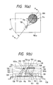
- Fig. 18(a) is a plane view of an optical pick-up apparatus in accordance with the sixth embodiment of the present invention
- Fig. 18(b) is a sectional view showing the optical pick-up apparatus in accordance with the sixth embodiment, taken along a line X-X of Fig. 18(a).
- a semiconductor laser chip 602 is mounted in parallel with and on a sensor substrate 601.
- the constitution of this reflection prism 604 and its vicinity is the same as the reflection prism 15 of the second embodiment and, therefore, will no more be explained in detail.
- This reflection prism 604, being trapezoidal shape, has a reflection surface confronting with the light emitting surface of the semiconductor laser chip 602.
- the laser beam having reached the reflection prism 604, is reflected at the reflection surface and enters as a diffusing or diverging beam 607 into the inside of a transparent light guide 605 through an incident window 606 formed on a second, i.e. a lower, surface 605b thereof.
- the light guide 605 is spaced from the semiconductor laser chip 602 and photo detectors 623, 629 later described.
- the light guide 605 has a first, i.e. an upper, surface 605a, disposed in parallel with the second surface 605b.
- the diffusing or diverging beam 607 reaches the holographic optical element 608, in which the diffusing or diverging beam 607 is diffracted.
- Adiffracted beam goes out of the light guide 605 and becomes a diffusing or diverging beam 609 consisting of 0-order diffraction beam.
- This diffusing or diverging beam 609 reaches a collimator lens 610 and is converted into a parallel beam 631 therethrough.
- This parallel beam 631 reaches an objective lens 630.
- the beam passing through the objective lens 630 becomes a focusing beam 613 and is focused on an information recording layer 611a of the optical disk 611 as a spot 612.
- the laser beam 603 emitted from the semiconductor laser chip 602 passes through the transparent light guide 605, diffusing normal to the first and second surfaces 605a, 605b thereof and, in turn, passes through the holographic optical element 608 disposed on the first surface 605a.
- the laser beam is converged along the axis normal to the first surface 605a of the light guide 605 onto the information recording layer 611a of the optical disk611 after passing through the collimator lens 610 and the objective lens 630.
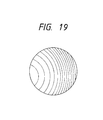
- the holographic optical element 608 has at least one hologram pattern shown in Fig. 19.
- This hologram pattern, shown in Fig. 19, has eccentric circles pattern, in which a center of these concentric circles positions at the center of the hologram pattern as shown in the drawing.
- This hologram pattern converts the laser beam, being reflected at the spot 612 and returning the same optical path as the going laser beam, into a returning diffraction beam 614 diffracted toward the second surface 605b with a predetermined incident angle.
- a returning optical path, starting from the optical disk 611, will be explained below.
- the laser beam having been reflected at the optical disk 611, reaches the objective lens 630 and is converted into a parallel beam, which advances toward the collimator lens 610.
- the leaser beam is, in turn, converted into a focusing beam by the collimator lens 610.
- the laser beam is subsequently converted into the returning diffraction beam 614 by the holographic optical element 608.
- the second surface 605b of the light guide 605 is formed with the returning-path polarized beam splitter 615.
- This returning-path polarized beam splitter 615 includes a polarized beam splitting film coated thereon, which can transmits P-polarized component and reflects S-polarized component of the returning diffraction beam 614.
- an arrow shown in Fig. 18(a) represents a linearly polarized beam 621, which expresses the polarization state of the diffusing beam 607 entered into the holographic optical element 608.
- the hologram pattern of the holographic optical element 608 is designed in such a mannerthat the diffraction direction of the returning diffraction beam 614 is inclined 45° with respect to the polarization direction of the linearly polarized beam 621. Accordingly, the returning diffraction beam 614 includes both P-polarized component and S-polarized component evenly, i.e. at a ratio of approximately 50 : 50.
- This transmission beam 622 is received by a first photo detector 623 provided on an upper surface of the sensor substrate 601.
- the remainder of the returning diffraction beam 614, after having been reflected at the returning-path polarized beam splitter 615, proceeds toward the first surface 605a as a reflection beam 624.
- the reflection beam 626 goes through a transmission window 627 formed on the second surface 605b and, subsequently, becomes a transmission beam 628.
- This transmission beam 628 is received by a second photo detector 629.
- the holographic optical element 608 and others are designed to let a focal point 630 of the returning diffraction beam 614 reside on an optical path between the returning-path polarized beam splitter 615 and the second photo detector 629.
- Figs. 20(a) and 20(b) show a modified construction of the sixth embodiment.
- a polarized beamsplitter auxiliary member 716 beneath a light guide 705.
- This auxiliary member 716 is transparent and directly connected to a second surface 705b of the lightguide 705.
- Arefrac- tive index of this auxiliary member 716 is substantially identical with that of the lightguide 705.
- This auxiliary member 716 increases a polarized beam splitting efficiency of the polarized beam splitter 715.
- a polarized beam splitter 715 can be completely surrounded by the light guide 705 and the auxiliary member 716. The application of this auxiliary member 716 brings a remarkable improvement in productivity.
- a space 718 With, it is no longer necessary to fill a space 718 with a transparent resin material or the like having substantially the same refractive index as the light guide 705. This space 718 is surrounded by the light guide 705 and a package 717.
- the package 717 is usually made of a non-conductive material such as ceramic.
- the remainder of components disclosed in the drawings are substantially the same as those of Figs. 18(a) and 18(b) and therefore will no more be explained.
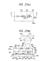
- Figs. 21 (a) and 21 (b) show still another modification of the sixth embodiment.
- Fig. 21(b) there is provided a objective lens 810 offinite system.
- the collimator lens 610 and the objective lens 630 of the sixth embodiment can be replaced by this infinite- system objective lens 810.
- Figs. 21 (a) and 21 (b) the remainder of components disclosed in the drawings are substantially the same as those of Figs. 18(a) and 18(b) and therefore will no more be explained.
- the inclined angle can be any of 45°, 135°, 225°, and 315°, i.e. an angle of (2n+1) 7 t/4 (n: integer).
Applications Claiming Priority (6)
| Application Number | Priority Date | Filing Date | Title |
|---|---|---|---|
| JP203345/92 | 1992-07-30 | ||
| JP4203346A JP2638403B2 (ja) | 1992-07-30 | 1992-07-30 | 光ピックアップ |
| JP4203345A JP2638402B2 (ja) | 1992-07-30 | 1992-07-30 | 光ピックアップ |
| JP203346/92 | 1992-07-30 | ||
| JP218948/92 | 1992-08-18 | ||
| JP21894892A JP3364955B2 (ja) | 1992-08-18 | 1992-08-18 | 光ピックアップ |
Publications (3)
| Publication Number | Publication Date |
|---|---|
| EP0581519A2 true EP0581519A2 (de) | 1994-02-02 |
| EP0581519A3 EP0581519A3 (de) | 1995-01-11 |
| EP0581519B1 EP0581519B1 (de) | 1998-05-27 |
Family
ID=27328225
Family Applications (1)
| Application Number | Title | Priority Date | Filing Date |
|---|---|---|---|
| EP93305753A Expired - Lifetime EP0581519B1 (de) | 1992-07-30 | 1993-07-21 | Optisches Wiedergabegerät |
Country Status (2)
| Country | Link |
|---|---|
| EP (1) | EP0581519B1 (de) |
| DE (1) | DE69318770T2 (de) |
Cited By (11)
| Publication number | Priority date | Publication date | Assignee | Title |
|---|---|---|---|---|
| DE4442976A1 (de) * | 1994-12-02 | 1996-06-05 | Thomson Brandt Gmbh | Vorrichtung zur berührungslosen optischen Abtastung von Informationen bei der Aufzeichnung auf und/oder Wiedergabe von einem Aufzeichnungsträger mit Aufzeichnungsspuren |
| EP0726568A2 (de) * | 1995-02-07 | 1996-08-14 | Fujitsu Limited | Für optische Speicherungseinheit verwendbares optisches Bauelement und optische Einrichtung damit |
| EP0729143A2 (de) * | 1995-02-24 | 1996-08-28 | Sony Corporation | Optische Vorrichtung |
| EP0762401A1 (de) * | 1995-08-22 | 1997-03-12 | Deutsche Thomson-Brandt Gmbh | Optische Abtasteinrichtung |
| WO1998013825A2 (en) * | 1996-09-27 | 1998-04-02 | Digital Optics Corporation | Integrated optical head apparatus and associated methods |
| US5886971A (en) * | 1996-09-27 | 1999-03-23 | Digital Optics Corporation | Optical head structures including support substrates adjacent transparent substrates and related methods |
| US5912872A (en) * | 1996-09-27 | 1999-06-15 | Digital Optics Corporation | Integrated optical apparatus providing separated beams on a detector and associated methods |
| WO2000048176A1 (fr) * | 1999-02-10 | 2000-08-17 | Rohm Co., Ltd. | Detecteur optique et dispositif d'hologramme |
| NL1014761C2 (nl) * | 1999-04-06 | 2004-07-15 | Nec Corp | Holografisch element. |
| CN100356464C (zh) * | 2004-11-17 | 2007-12-19 | 上海乐金广电电子有限公司 | 光盘拾取器的集成基础光学系统 |
| US8153957B2 (en) | 1996-09-27 | 2012-04-10 | Digitaloptics Corporation East | Integrated optical imaging systems including an interior space between opposing substrates and associated methods |
Citations (5)
| Publication number | Priority date | Publication date | Assignee | Title |
|---|---|---|---|---|
| EP0195657A2 (de) * | 1985-03-20 | 1986-09-24 | Fujitsu Limited | Optische Abtastvorrichtung |
| EP0278406A2 (de) * | 1987-02-06 | 1988-08-17 | Sony Corporation | Optischer Lesekopf |
| EP0467303A2 (de) * | 1990-07-16 | 1992-01-22 | Matsushita Electric Industrial Co., Ltd. | Kopf für optische Platte und Verfahren zu seiner Herstellung |
| EP0469552A2 (de) * | 1990-07-31 | 1992-02-05 | Omron Corporation | Optisches Wiedergabegerät |
| US5122903A (en) * | 1989-03-15 | 1992-06-16 | Omron Corporation | Optical device and optical pickup device using the same |
Family Cites Families (3)
| Publication number | Priority date | Publication date | Assignee | Title |
|---|---|---|---|---|
| JPH06101137B2 (ja) * | 1986-03-20 | 1994-12-12 | 富士通株式会社 | 光ピツクアツプ |
| JPS63247925A (ja) * | 1987-04-01 | 1988-10-14 | Hitachi Ltd | 光ヘツド |
| JPH01155529A (ja) * | 1987-12-11 | 1989-06-19 | Seiko Epson Corp | 光ピックアップ |
-
1993
- 1993-07-21 EP EP93305753A patent/EP0581519B1/de not_active Expired - Lifetime
- 1993-07-21 DE DE69318770T patent/DE69318770T2/de not_active Expired - Fee Related
Patent Citations (5)
| Publication number | Priority date | Publication date | Assignee | Title |
|---|---|---|---|---|
| EP0195657A2 (de) * | 1985-03-20 | 1986-09-24 | Fujitsu Limited | Optische Abtastvorrichtung |
| EP0278406A2 (de) * | 1987-02-06 | 1988-08-17 | Sony Corporation | Optischer Lesekopf |
| US5122903A (en) * | 1989-03-15 | 1992-06-16 | Omron Corporation | Optical device and optical pickup device using the same |
| EP0467303A2 (de) * | 1990-07-16 | 1992-01-22 | Matsushita Electric Industrial Co., Ltd. | Kopf für optische Platte und Verfahren zu seiner Herstellung |
| EP0469552A2 (de) * | 1990-07-31 | 1992-02-05 | Omron Corporation | Optisches Wiedergabegerät |
Non-Patent Citations (3)
| Title |
|---|
| PATENT ABSTRACTS OF JAPAN vol. 12, no. 86 (P-677) 18 March 1988 & JP-A-62 219 341 (FUJITSU LTD) 26 September 1987 * |
| PATENT ABSTRACTS OF JAPAN vol. 13, no. 424 (P-934) 21 September 1989 & JP-A-01 155 529 (SEIKO EPSOM CORP) 19 June 1989 * |
| PATENT ABSTRACTS OF JAPAN vol. 13, no. 57 (P-825) 9 February 1989 & JP-A-63 247 925 (HITACHI LTD) 14 October 1988 * |
Cited By (21)
| Publication number | Priority date | Publication date | Assignee | Title |
|---|---|---|---|---|
| DE4442976A1 (de) * | 1994-12-02 | 1996-06-05 | Thomson Brandt Gmbh | Vorrichtung zur berührungslosen optischen Abtastung von Informationen bei der Aufzeichnung auf und/oder Wiedergabe von einem Aufzeichnungsträger mit Aufzeichnungsspuren |
| EP0726568A2 (de) * | 1995-02-07 | 1996-08-14 | Fujitsu Limited | Für optische Speicherungseinheit verwendbares optisches Bauelement und optische Einrichtung damit |
| EP0726568A3 (de) * | 1995-02-07 | 1997-02-26 | Fujitsu Ltd | Für optische Speicherungseinheit verwendbares optisches Bauelement und optische Einrichtung damit |
| US5745265A (en) * | 1995-02-07 | 1998-04-28 | Fujitsu Limited | Optical element utilized for optical storage unit and optical device including the optical element |
| EP0729143A2 (de) * | 1995-02-24 | 1996-08-28 | Sony Corporation | Optische Vorrichtung |
| EP0729143A3 (de) * | 1995-02-24 | 1996-09-04 | Sony Corp | |
| US5703861A (en) * | 1995-02-24 | 1997-12-30 | Sony Corporation | Integrated confocal optical pick-up head with a hologram and a polarizer mounted on each side of a transparent heat sink |
| EP0762401A1 (de) * | 1995-08-22 | 1997-03-12 | Deutsche Thomson-Brandt Gmbh | Optische Abtasteinrichtung |
| CN1096065C (zh) * | 1995-08-22 | 2002-12-11 | 德国汤姆逊-布朗特公司 | 光学扫描装置 |
| US5872762A (en) * | 1996-09-27 | 1999-02-16 | Digital Optics Corporation | Optical head structures including electronic devices adjacent transparent substrates and related methods |
| WO1998013825A3 (en) * | 1996-09-27 | 1998-08-06 | Digital Optics Corp | Integrated optical head apparatus and associated methods |
| US5886971A (en) * | 1996-09-27 | 1999-03-23 | Digital Optics Corporation | Optical head structures including support substrates adjacent transparent substrates and related methods |
| US5912872A (en) * | 1996-09-27 | 1999-06-15 | Digital Optics Corporation | Integrated optical apparatus providing separated beams on a detector and associated methods |
| US6104690A (en) * | 1996-09-27 | 2000-08-15 | Digital Optics Corporation | Integrated optical apparatus and associated methods |
| WO1998013825A2 (en) * | 1996-09-27 | 1998-04-02 | Digital Optics Corporation | Integrated optical head apparatus and associated methods |
| US6522618B1 (en) | 1996-09-27 | 2003-02-18 | Digital Optics Corp. | Integrated optical apparatus and associated methods |
| US8153957B2 (en) | 1996-09-27 | 2012-04-10 | Digitaloptics Corporation East | Integrated optical imaging systems including an interior space between opposing substrates and associated methods |
| WO2000048176A1 (fr) * | 1999-02-10 | 2000-08-17 | Rohm Co., Ltd. | Detecteur optique et dispositif d'hologramme |
| US6335809B1 (en) | 1999-02-10 | 2002-01-01 | Rohm Co., Ltd. | Optical pickup and hologram device |
| NL1014761C2 (nl) * | 1999-04-06 | 2004-07-15 | Nec Corp | Holografisch element. |
| CN100356464C (zh) * | 2004-11-17 | 2007-12-19 | 上海乐金广电电子有限公司 | 光盘拾取器的集成基础光学系统 |
Also Published As
| Publication number | Publication date |
|---|---|
| EP0581519A3 (de) | 1995-01-11 |
| DE69318770D1 (de) | 1998-07-02 |
| EP0581519B1 (de) | 1998-05-27 |
| DE69318770T2 (de) | 1998-10-15 |
Similar Documents
| Publication | Publication Date | Title |
|---|---|---|
| US5410468A (en) | Optical pick-up apparatus | |
| EP0581519A2 (de) | Optisches Wiedergabegerät | |
| US7274632B2 (en) | Optical head device and method for correcting spherical aberration | |
| CA2002381C (en) | Optical pickup device | |
| EP0469580B1 (de) | Optisches Abtastgerät | |
| US5745304A (en) | Integrated optical pickup system capable of reading optical disks of different thickness | |
| US5406532A (en) | Optical system for a magneto-optical recording/reproducing apparatus | |
| EP0774751B1 (de) | Optische Abtastvorrichtung zur Wiedergabe von unterschiedlichen optischen Platten | |
| US6278560B1 (en) | Optical scanning device | |
| JPS6117103A (ja) | 偏光ビ−ムスプリツタ | |
| JPH02265036A (ja) | 光学ヘッド | |
| US4733277A (en) | Apparatus for reproducing information from an optical disk | |
| JPH0337837A (ja) | 光デイスクのチルト検出装置 | |
| JPH0264917A (ja) | 光磁気記録装置用光学ヘッド構造 | |
| JP2638403B2 (ja) | 光ピックアップ | |
| JP2718326B2 (ja) | 光ピックアップ | |
| JPH0242642A (ja) | 光学ヘッド構造 | |
| JP2638402B2 (ja) | 光ピックアップ | |
| JP3364955B2 (ja) | 光ピックアップ | |
| JPH10233031A (ja) | 光学ピックアップ装置及びその調整方法 | |
| JP2709090B2 (ja) | 導波路型光学ヘッド | |
| JPH0487041A (ja) | 光学ピックアップ装置 | |
| JPH0264919A (ja) | 光学ヘッド構造 | |
| JPH0242641A (ja) | 光学ヘッド構造 | |
| JPS6111951A (ja) | 光ヘツド装置 |
Legal Events
| Date | Code | Title | Description |
|---|---|---|---|
| PUAI | Public reference made under article 153(3) epc to a published international application that has entered the european phase |
Free format text: ORIGINAL CODE: 0009012 |
|
| 17P | Request for examination filed |
Effective date: 19930729 |
|
| AK | Designated contracting states |
Kind code of ref document: A2 Designated state(s): DE FR GB NL |
|
| PUAL | Search report despatched |
Free format text: ORIGINAL CODE: 0009013 |
|
| AK | Designated contracting states |
Kind code of ref document: A3 Designated state(s): DE FR GB NL |
|
| 17Q | First examination report despatched |
Effective date: 19970211 |
|
| GRAG | Despatch of communication of intention to grant |
Free format text: ORIGINAL CODE: EPIDOS AGRA |
|
| GRAG | Despatch of communication of intention to grant |
Free format text: ORIGINAL CODE: EPIDOS AGRA |
|
| GRAH | Despatch of communication of intention to grant a patent |
Free format text: ORIGINAL CODE: EPIDOS IGRA |
|
| GRAH | Despatch of communication of intention to grant a patent |
Free format text: ORIGINAL CODE: EPIDOS IGRA |
|
| GRAA | (expected) grant |
Free format text: ORIGINAL CODE: 0009210 |
|
| AK | Designated contracting states |
Kind code of ref document: B1 Designated state(s): DE FR GB NL |
|
| REF | Corresponds to: |
Ref document number: 69318770 Country of ref document: DE Date of ref document: 19980702 |
|
| ET | Fr: translation filed | ||
| PLBE | No opposition filed within time limit |
Free format text: ORIGINAL CODE: 0009261 |
|
| STAA | Information on the status of an ep patent application or granted ep patent |
Free format text: STATUS: NO OPPOSITION FILED WITHIN TIME LIMIT |
|
| 26N | No opposition filed | ||
| PGFP | Annual fee paid to national office [announced via postgrant information from national office to epo] |
Ref country code: FR Payment date: 20000711 Year of fee payment: 8 |
|
| PGFP | Annual fee paid to national office [announced via postgrant information from national office to epo] |
Ref country code: DE Payment date: 20000717 Year of fee payment: 8 |
|
| PGFP | Annual fee paid to national office [announced via postgrant information from national office to epo] |
Ref country code: GB Payment date: 20000719 Year of fee payment: 8 |
|
| PG25 | Lapsed in a contracting state [announced via postgrant information from national office to epo] |
Ref country code: GB Free format text: LAPSE BECAUSE OF NON-PAYMENT OF DUE FEES Effective date: 20010721 |
|
| GBPC | Gb: european patent ceased through non-payment of renewal fee |
Effective date: 20010721 |
|
| PG25 | Lapsed in a contracting state [announced via postgrant information from national office to epo] |
Ref country code: FR Free format text: LAPSE BECAUSE OF NON-PAYMENT OF DUE FEES Effective date: 20020329 |
|
| PG25 | Lapsed in a contracting state [announced via postgrant information from national office to epo] |
Ref country code: DE Free format text: LAPSE BECAUSE OF NON-PAYMENT OF DUE FEES Effective date: 20020501 |
|
| REG | Reference to a national code |
Ref country code: FR Ref legal event code: ST |
|
| PGFP | Annual fee paid to national office [announced via postgrant information from national office to epo] |
Ref country code: NL Payment date: 20050703 Year of fee payment: 13 |
|
| PG25 | Lapsed in a contracting state [announced via postgrant information from national office to epo] |
Ref country code: NL Free format text: LAPSE BECAUSE OF NON-PAYMENT OF DUE FEES Effective date: 20070201 |
|
| NLV4 | Nl: lapsed or anulled due to non-payment of the annual fee |
Effective date: 20070201 |