EP0774751B1 - Optische Abtastvorrichtung zur Wiedergabe von unterschiedlichen optischen Platten - Google Patents
Optische Abtastvorrichtung zur Wiedergabe von unterschiedlichen optischen Platten Download PDFInfo
- Publication number
- EP0774751B1 EP0774751B1 EP96118267A EP96118267A EP0774751B1 EP 0774751 B1 EP0774751 B1 EP 0774751B1 EP 96118267 A EP96118267 A EP 96118267A EP 96118267 A EP96118267 A EP 96118267A EP 0774751 B1 EP0774751 B1 EP 0774751B1
- Authority
- EP
- European Patent Office
- Prior art keywords
- optical disk
- pickup device
- reflection
- reflection beam
- optical
- Prior art date
- Legal status (The legal status is an assumption and is not a legal conclusion. Google has not performed a legal analysis and makes no representation as to the accuracy of the status listed.)
- Expired - Lifetime
Links
- 230000003287 optical effect Effects 0.000 title claims description 379
- 230000002093 peripheral effect Effects 0.000 claims description 73
- 230000010287 polarization Effects 0.000 claims description 62
- 238000001514 detection method Methods 0.000 claims description 18
- 239000004973 liquid crystal related substance Substances 0.000 claims description 13
- 238000010586 diagram Methods 0.000 description 18
- 238000000034 method Methods 0.000 description 8
- 238000009826 distribution Methods 0.000 description 7
- 230000007246 mechanism Effects 0.000 description 5
- 230000009467 reduction Effects 0.000 description 5
- 230000012447 hatching Effects 0.000 description 4
- 239000004065 semiconductor Substances 0.000 description 4
- 239000000853 adhesive Substances 0.000 description 3
- 101710170230 Antimicrobial peptide 1 Proteins 0.000 description 2
- 101710170231 Antimicrobial peptide 2 Proteins 0.000 description 2
- 230000004075 alteration Effects 0.000 description 2
- 230000008859 change Effects 0.000 description 2
- 238000007796 conventional method Methods 0.000 description 2
- 239000006059 cover glass Substances 0.000 description 2
- 238000004519 manufacturing process Methods 0.000 description 2
- 230000000903 blocking effect Effects 0.000 description 1
- 150000001875 compounds Chemical class 0.000 description 1
- 230000001419 dependent effect Effects 0.000 description 1
- 238000002474 experimental method Methods 0.000 description 1
- 230000002401 inhibitory effect Effects 0.000 description 1
- 238000012986 modification Methods 0.000 description 1
- 230000004048 modification Effects 0.000 description 1
- 230000008569 process Effects 0.000 description 1
Images


Classifications
-
- G—PHYSICS
- G11—INFORMATION STORAGE
- G11B—INFORMATION STORAGE BASED ON RELATIVE MOVEMENT BETWEEN RECORD CARRIER AND TRANSDUCER
- G11B7/00—Recording or reproducing by optical means, e.g. recording using a thermal beam of optical radiation by modifying optical properties or the physical structure, reproducing using an optical beam at lower power by sensing optical properties; Record carriers therefor
- G11B7/12—Heads, e.g. forming of the optical beam spot or modulation of the optical beam
- G11B7/13—Optical detectors therefor
- G11B7/131—Arrangement of detectors in a multiple array
-
- G—PHYSICS
- G11—INFORMATION STORAGE
- G11B—INFORMATION STORAGE BASED ON RELATIVE MOVEMENT BETWEEN RECORD CARRIER AND TRANSDUCER
- G11B7/00—Recording or reproducing by optical means, e.g. recording using a thermal beam of optical radiation by modifying optical properties or the physical structure, reproducing using an optical beam at lower power by sensing optical properties; Record carriers therefor
- G11B7/12—Heads, e.g. forming of the optical beam spot or modulation of the optical beam
- G11B7/123—Integrated head arrangements, e.g. with source and detectors mounted on the same substrate
-
- G—PHYSICS
- G11—INFORMATION STORAGE
- G11B—INFORMATION STORAGE BASED ON RELATIVE MOVEMENT BETWEEN RECORD CARRIER AND TRANSDUCER
- G11B7/00—Recording or reproducing by optical means, e.g. recording using a thermal beam of optical radiation by modifying optical properties or the physical structure, reproducing using an optical beam at lower power by sensing optical properties; Record carriers therefor
- G11B7/12—Heads, e.g. forming of the optical beam spot or modulation of the optical beam
- G11B7/135—Means for guiding the beam from the source to the record carrier or from the record carrier to the detector
- G11B7/1353—Diffractive elements, e.g. holograms or gratings
-
- G—PHYSICS
- G11—INFORMATION STORAGE
- G11B—INFORMATION STORAGE BASED ON RELATIVE MOVEMENT BETWEEN RECORD CARRIER AND TRANSDUCER
- G11B7/00—Recording or reproducing by optical means, e.g. recording using a thermal beam of optical radiation by modifying optical properties or the physical structure, reproducing using an optical beam at lower power by sensing optical properties; Record carriers therefor
- G11B7/12—Heads, e.g. forming of the optical beam spot or modulation of the optical beam
- G11B7/135—Means for guiding the beam from the source to the record carrier or from the record carrier to the detector
- G11B7/1359—Single prisms
-
- G—PHYSICS
- G11—INFORMATION STORAGE
- G11B—INFORMATION STORAGE BASED ON RELATIVE MOVEMENT BETWEEN RECORD CARRIER AND TRANSDUCER
- G11B7/00—Recording or reproducing by optical means, e.g. recording using a thermal beam of optical radiation by modifying optical properties or the physical structure, reproducing using an optical beam at lower power by sensing optical properties; Record carriers therefor
- G11B7/12—Heads, e.g. forming of the optical beam spot or modulation of the optical beam
- G11B7/135—Means for guiding the beam from the source to the record carrier or from the record carrier to the detector
- G11B7/1381—Non-lens elements for altering the properties of the beam, e.g. knife edges, slits, filters or stops
-
- G—PHYSICS
- G11—INFORMATION STORAGE
- G11B—INFORMATION STORAGE BASED ON RELATIVE MOVEMENT BETWEEN RECORD CARRIER AND TRANSDUCER
- G11B7/00—Recording or reproducing by optical means, e.g. recording using a thermal beam of optical radiation by modifying optical properties or the physical structure, reproducing using an optical beam at lower power by sensing optical properties; Record carriers therefor
- G11B2007/0003—Recording, reproducing or erasing systems characterised by the structure or type of the carrier
- G11B2007/0006—Recording, reproducing or erasing systems characterised by the structure or type of the carrier adapted for scanning different types of carrier, e.g. CD & DVD
Definitions
- the present invention relates to an optical pickup device which detects a reflection beam from an optical disk and generates a read-data signal based on the reflection beam.
- a conventional optical pickup device for reading out data from an optical disk is known.
- a laser beam is emitted by a semiconductor laser to the optical disk.
- the emission beam from the semiconductor laser is converted into a converging beam by an objective lens, the converging beam passing through a transparent layer of the optical disk and forming a light spot on a recording surface of the optical disk.
- a photodetecting unit generates a signal indicative of read-out data by detecting a reflection beam from the optical disk.
- optical disks such as compact disks (CD) are widely used to store information and reproduce the information.
- two different types of the optical disks will come to be popular: a standard recording-density optical disk and a high recording-density optical disk.
- One of the basic requirements for these optical disks is that the standard recording-density type has a transparent layer which is about 1.2 mm thick, and the high recording-density type has a transparent layer which is about 0.6 mm thick.
- optical pickup device which can access the standard recording-density optical disk and the high recording-density optical disk in common by using the same pickup device, in order to enable data to be read out from each of the two optical disks.
- an emission beam from the semiconductor laser is converted into a converging beam by the objective lens, the converging beam passing through the transparent layer of the optical disk and forming a light spot on the recording surface of the optical disk.
- the diameter of the light spot has to be about 1.5 ⁇ m.
- the diameter of the light spot has to be about 0.95 ⁇ m.
- optical characteristics e.g., spherical aberration
- the optical characteristics of the objective lens are preset depending on the smaller thickness of the transparent layer of the high recording-density optical disk.
- the converging beam from the objective lens can correctly pass through the transparent layer (the thickness: about 0.6 mm) of the optical disk and form a light spot which is suited to the requirement for the high recording-density type.
- the converging beam from the above objective lens cannot suitably pass through the transparent layer (the thickness: about 1.2 mm) of the optical disk and form a light spot which is suited to the standard recording-density optical disk.
- the converging beam from the above objective lens does not converge on the recording surface of the standard recording-density optical disk. Since the spherical aberration is poor due to the different thickness of the transparent layer of the optical disk, a suitably focused light on the recording surface of the optical disk is not formed.
- an aperture unit with an opening is placed on an optical path of the emission beam from the objective lens to the optical disk when the standard recording-density optical disk is accessed.
- the aperture unit has not to be placed when the high recording-density optical disk is accessed.
- the aperture unit is placed on the optical path of the emission beam. This allows a desired portion of the converging beam from the objective lens to be directed to the optical disk, but inhibits an undesired portion of the converging beam from entering the optical disk, so as to avoid the above-described problem.
- the position at which the aperture unit is placed on the optical path of the emission beam requires a very high accuracy.
- the above optical pickup device include an aperture moving mechanism which very accurately moves the aperture unit onto the optical path of the emission beam.
- an additional process for producing the aperture moving mechanism must be performed.
- the aperture moving mechanism and the aperture unit must require a very high accuracy of the assembly. Therefore, the above-described optical pickup device is not useful to reduce the cost of the optical pickup device or allow efficient production processes thereof.
- EP 0 610 055 A2 on which the preamble of claim 1 is based, discloses an optical pickup device for optionally accessing a thick optical disk or a thin optical disk.
- the optical pickup device comprises a compound objective lens that has two focal points so that two diffraction-limited converging spots can be simultaneously formed from an incident light beam at two different focal lengths.
- an objective lens with a hologram grating is used.
- the hologram lens diffracts and refracts a first part of incident light to thereby form a first focal point.
- the rest of the incident light is transmitted through the hologram grating undiffracted to thereby form the second focal point.
- the diffraction efficiency of the hologram grating cannot be 100%, a part of the transmitted (or diffracted) incident light beam will always be imaged onto the photo detector used to detect the diffracted (or transmitted) part of the incident light beam after reflection from the information-recording layer of the optical disk. This results in a certain noise in the information signal, the focus-error signal and the track-error signal.
- WO 96/28816 which is prior art according to Art.
- 54(3) EPC for the designated states DE and FR discloses an optical scanning device that can scan a first type of optical disk, which is relatively thin, and a second type of optical disk, which is thicker.
- the information layer of the thick optical disk is scanned by means of a converting light beam, when the information layer is arranged axially not at the best position of the best focus but near the position of the paraxial focus. Accordingly, for the detection of an information signal from the thick optical disk only the central portion of the reflected light beam is used, whereas for the detection of an information signal from the thin optical disk both the central and the peripheral portion of the reflected light beam is used.
- This document discloses the use of adjustable blocking means allowing to block a ring shaped peripheral portion of the reflection beam.
- EP 0 737 964 A1 which is prior art according to Art. 54(3) EPC for the designated states DE and FR, discloses an optical disk apparatus using the conventional method as discussed above, wherein a beam limiting means, i.e. an aperture, is disposed in the light beam incident onto the optical disk, for limiting the numerical aperture of the incident convergent optical beam directed to the information layer of the optical disk.
- the numerical aperture of the limiting means can be changed.
- the beam limiting means acts both on the reflection beam from the optical disk and on the light beam from the light source towards the optical disk.
- optical pickup device comprising the features of claim 1. Further advantageous embodiments are the subject matter of the dependent claims.
- the optical pickup device of the present invention can effectively access each of first and second optical disks having transparent layers with different thicknesses without producing an undesired reduction of the amplitude of the signal generated by the photodetecting unit. Further, it is possible for the present invention to provide a capability for the optical pickup device to effectively generate a read-data signal from each of the two optical disks by using the same device.
- FIGS.1A through 1F show an optical pickup device to which one embodiment of the present invention is applied.
- an emission beam emitted by a laser diode (or a semiconductor laser) 1 is converted into a parallel beam by a collimator lens 2.
- the parallel beam passes through a beam splitter 3, and it is deflected by a deflection prism 4 to an optical disk.
- the deflected beam from the deflection prism 4 is converted into a converging beam by an objective lens 5.
- the converging beam from the objective lens 5 passes through a transparent layer of the optical disk, and a light spot on the recording surface of the optical disk is formed.
- a reflection beam from the optical disk passes through the objective lens 5, and it is deflected by the deflection prism 4 to the beam splitter 3.
- the reflection beam from the deflection prism 4 is reflected by the beam splitter 3 to an aperture unit 9.
- the reflection beam passed through the aperture unit 9 is converted into a converging beam by a detecting lens 7.
- the converging beam from the detecting lens 7 enters a photodiode 8.
- the photodiode 8 generates a signal indicative of read-out data based on the reflection beam from the optical disk.
- the reflection beam passes through the aperture unit 9 between the beam splitter 3 and the detecting lens 7.
- the optical disk shown in FIG.1A is a high-recording-density optical disk 6A having a recording surface 60 and a first transparent layer.
- the first transparent layer is about 0.6 mm thick.
- FIG.1B shows a standard-recording-density optical disk 6B.
- the standard-recording-density optical disk 6B has a recording surface 61 and a second transparent layer.
- the second transparent layer is about 1.2 mm thick.
- the thickness of the second transparent layer of the optical disk 6B is greater than the thickness of the first transparent layer of the optical disk 6A.
- FIG.1C shows the aperture unit 9 of the optical pickup device in FIG.1A.
- the aperture unit 9 in the present embodiment is a light-shading plate having a circular opening 9A.
- the light-shading plate is indicated by hatching lines in FIG.1C.
- the aperture unit 9 in FIG.1C is placed on the optical path between the beam splitter 3 and the detecting lens 7. At this time, the aperture unit 9 is set in a light-shading condition in which a peripheral portion of the reflection beam from the beam splitter 3 is cut off by the light-shading plate of the aperture unit 9. A central portion of the reflection beam passes through the opening 9A of the aperture unit 9 to the photodiode 8.
- the aperture unit 9 is set in a non-shading condition. At this time, both the central portion and the peripheral portion of the reflection beam are allowed to pass through the aperture unit 9 to the photodiode 8.
- the aperture unit 9 converts the reflection beam directed to the photodiode 8 such that the central portion and the peripheral portion of the reflection beam are allowed to enter the photodiode 8 when the optical disk 6A is accessed, and the central portion is allowed to enter the photodiode 8 and the peripheral portion is inhibited from entering the photodiode 8 when the optical disk 6B is accessed.
- a focus error detecting unit which outputs a focus error signal and/or a tracking error detecting unit which outputs a tracking error signal are provided. These detecting units output the error signals separately from a read-data signal generated by the photodiode 8 based on the reflection beam from the optical disk.
- the focus error detecting unit and the tracking error detecting unit are not shown in FIG.1A and a description thereof will be omitted for the sake of convenience.
- the high-recording-density optical disk 6A has, as shown in FIG.1D, the recording surface 60 and the first transparent layer.
- the emission beam from the objective lens 5 passes through the first transparent layer to the recording surface 60, and the distance that the emission beam has to transmit for the optical disk 6A is the thickness of the first transparent layer which is about 0.6 mm.
- the optical characteristics of the objective lens 5 in the present embodiment are set depending on the thickness of the first transparent layer of the optical disk 6A. Therefore, when the optical disk 6A is accessed, the emission beam is converted into a converting beam by the objective lens 5, and a light spot on the recording surface 60 of the optical disk 6A is correctly formed, as shown in FIG.1D.
- the standard-recording-density optical disk 6B has, as shown in FIG.1E, the recording surface 61 and the second transparent layer.
- the emission beam from the objective lens 5 passes through the second transparent layer to the recording surface 61, and the distance that the emission beam has to transmit for the optical disk 6B is the thickness of the second transparent layer which is about 1.2 mm.
- FIG.1F shows a light spot "SP" which is formed on the recording surface 61 of the optical disk 6B by the emission beam from the objective lens 5.
- a central area "SP1" of the light spot SP is produced by the central portion (the converging portion) of the emission beam from the objective lens 5.
- the intensity of the central area SP1 is relatively great.
- a peripheral area "SP2" of the light spot SP is produced by the peripheral portion (the non-converging portion) of the emission beam from the objective lens 5.
- the central area SP1 is surrounded by the peripheral area SP2.
- the intensity of the peripheral area SP2 is relatively small.
- the peripheral portion of the emission beam from the objective lens 5 forms the non-converging portion of the light spot on the recording surface 61 of the optical disk 6B.
- the reflection beam from the recording surface 61 of the optical disk 6B also includes a peripheral portion, and such a peripheral portion of the reflection beam passes through the objective lens 5 to the photodiode 8.
- FIGS.2A and 2B show cross-sectional distributions of intensity of the reflection beam when the standard-recording-density optical disk 6B is accessed by the optical pickup device.
- the intensity of the reflection beam for white areas is very small, and the intensity of the reflection beam for dotted areas is varied in proportion with the density of dots indicated.
- the intensity of the reflection beam for areas in which the dot density in FIGS.2A and 2B is small is relative small, and the intensity of the reflection beam for areas in which the dot density in FIGS.2A and 2B is great is relatively great.
- the intensity of the reflection beam has the cross-sectional distribution, shown in FIG.2A, when the light spot SP is located at an interval between pits on a track of the optical disk 6B.
- the intensity of the reflection beam has the cross-sectional distribution, shown in FIG.2B, when the light spot SP is located at the center of a pit on the track of the optical disk 6B.
- FIG.3 shows a change in the amplitude of a signal generated by a photodetector when the position of the light spot SP on the track of the optical disk 6B is moved from the interval to the interval via the center of the pit.
- the amplitude of the signal is changed as indicated by a curve "2-1" in FIG.3.
- the amplitude of the signal is the smallest (or the lower peak) when the light spot SP is located at the center of the pit, and it is the greatest (or the upper peak) when the light spot SP is located at the interval.
- a difference "AMP1" between the upper peak and the lower peak on the curve "2-1" in FIG.3 is relatively small.
- the aperture unit 9 is not placed on the optical path when the optical disk 6B is accessed, it is difficult for the optical pickup device to effectively read out the pit on the track of the optical disk 6B since the difference AMP1 in the amplitude of the signal is relatively small.
- the aperture unit 9 since the aperture unit 9 is placed on the optical path when the optical disk 6B is accessed, the areas 2A in the peripheral portion of the reflection beam are eliminated by the aperture unit 9.
- the amplitude of the signal generated by the photodiode 8 is changed as indicated by a curve "2-2" in FIG.3.
- the difference between the upper peak and the lower peak on the curve "2-2" can be increased to a relatively great difference "AMP2" as shown in FIG.3.
- the optical pickup device of the present invention utilizes the aperture unit 9 and it can effectively read out the data from the standard-recording-density optical disk 6B.
- the high-recording-density optical disk 6A is accessed, the light spot on the recording surface of the optical disk 6A is correctly formed, but the amplitude of the signal generated by the photodiode 8 is reduced due to the aperture unit 9.
- a waveform equalizer circuit may be added to the optical pickup device of the present embodiment.
- the amplitude of the signal generated by the photodiode 8 can be electrically corrected by the waveform equalizer circuit.
- the aperture unit 9 is arranged at a fixed position relative to the optical pickup device.
- a setting unit 10 connected to the aperture unit 9 is further included.
- the setting unit 10 is indicated by a dotted line, which shows that the setting unit 10 may or may not be used by the optical pickup device of the present embodiment.
- the setting unit 10 sets the aperture unit 9 in one of a first condition (the non-shading condition) in which the central portion and the peripheral portion of the reflection beam directed to the photodiode 8 are allowed to enter the photodiode 8 and a second condition (the light-shading condition) in which the peripheral portion is inhibited from entering the photodiode 8 and only the central portion is allowed to enter the photodiode 8.
- the setting unit 10 sets the aperture unit 9 in the first condition, and the central portion and the peripheral portion are not shaded by the light-shading plate of the aperture unit 9 and they are allowed to pass through the opening 9A to the photodiode 8.
- the setting unit 10 sets the aperture unit 9 in the second condition, and the peripheral portion is shaded by the light-shading plate but the central portion is allowed to pass through the opening 9A to the photodiode 8.
- the optical pickup device of the present embodiment can effectively read out the data from each of the optical disk 6B and the optical disk 6A.
- the aperture unit 9 has the light-shading plate with the opening 9A.
- the setting unit 10 is a moving mechanism for moving the light-shading plate of the aperture unit 10.
- the light-shading plate is placed on an optical path of the reflection beam directed to the photodiode 8, thereby the light-shading place inhibiting the peripheral portion from entering the photodiode 8.
- the moving mechanism mentioned above may be a solenoid-actuation type which is capable of shifting the light-shading plate by using an actuation force of a solenoid coil, or a motor-drive type which is capable of rotating or swinging the light-shading plate by using a driving force of a motor.
- the positional relation between the opening of the aperture unit 9 and the reflection beam must be accurately set.
- the accuracy of the positional relation when the light-shading plate is placed on the optical path of the reflection beam directed to the photodiode 8 is lower than the accuracy of the positional relation when an aperture unit is placed on the optical path of the emission beam directed to the optical disk as in the conventional device.
- the accuracy of the positional relation can be reduced to a reasonable level.
- FIGS.4A and 4B show a liquid-crystal shutter 90 which is used as another example of the aperture unit 9.
- reference numeral 100 indicates the reflection beam which is directed to the photodiode 8 by the beam splitter 3.
- a portion of the liquid-crystal shutter 90 which is set in an opaque condition is indicated by hatching lines in FIG.4A.
- FIG.4B the liquid-crystal shutter 90 which is set in a transparent condition is indicated.
- the liquid-crystal shutter 90 has an opening, and the liquid-crystal shutter 90 is electrically set in one of the transparent condition (FIG.4B) and the opaque condition (FIG.4A).
- the liquid-crystal shutter 90 is electrically set in the transparent condition, and the central portion and the peripheral portion of the reflection beam 100 are allowed to pass through the shutter 90 to the photodiode 8.
- the liquid-crystal shutter 90 is set in the opaque condition, and the peripheral portion is inhibited by the shutter 90 from entering the photodiode 8 and only the central portion is allowed to pass through the opening to the photodiode 8.
- each of the aperture unit 9 and the liquid-crystal shutter 90 has the opening shaped into a circle.
- the aperture unit 9 of the present invention is not limited to these embodiments.
- An aperture unit having a light-shading plate with an opening, the opening being shaped into an ellipse, may be suitably used by the optical pickup device of the present invention.
- FIG.5 shows an aperture unit 91 which is an alternative of the aperture unit 9 for use in the optical pickup device in FIG.1A.
- a direction parallel to a track of the optical disk is indicated by an arrow "A”
- a direction perpendicular to the direction of the track of the optical disk is indicated by an arrow "B”.
- the aperture unit 91 has a rectangular opening 91A and a pair of upper and lower light-shading plates 91B and 91C on both sides of the opening 91A.
- the opening 91A extends in the direction "A" parallel to a track of the optical disk.
- the upper and lower light-shading plates 91B and 91C are arranged in the direction "B" perpendicular to the track of the optical disk.
- the light-shading plates 91B and 91C cut off the peripheral portion of the reflection beam directed to the photodiode 8 when each of the optical disks 6A and 6B is accessed.
- the above aperture unit 91 has an advantageous feature which will be described below with reference to FIGS.6A, 6B and 6C.
- FIG.6A shows the reflection beam 100 which is directed to the photodiode 8 when the optical disk 6A is accessed and the light spot of the corresponding emission beam is located at the center of a pit of the optical disk 6A.
- FIG.6B shows the reflection beam 100 which is directed to the photodiode 8 when the optical disk 6A is accessed and the light spot is located at the interval between pits of the optical disk 6A.
- areas with a relatively great intensity considerably influencing the generation of a read-data signal by the photodiode 8, which are indicated hatching lines in FIG.6B extend over the central portion to the peripheral portion of the reflection beam 100. Since the recording density of the optical disk 6A is high and the interval between the pits is small, the diffraction angles of the 0th and lst order diffraction rays of the reflection beam 100 become great.
- the amplitude of the read-data signal generated by the photodiode 8 when the light spot is located at the interval of the optical disk 6A is considerably reduced. Therefore, in such a case, the generation of the read-data signal by the photodetector 8 when the optical disk 6A having the transparent layer with the smaller thickness is accessed is considerably influenced.
- the peripheral portion of the reflection beam 100 is cut off by the aperture unit 91 having the rectangular opening 91A and the light-shading plates 91B and 91C, the undesired reduction of the amplitude of the read-data signal generated by the photodiode 8 when the light spot is located at the interval of the optical disk 6A can be avoided. This is because the areas with a relatively great intensity in the reflection beam 100 are not shaded by the aperture unit 91 of the present embodiment.
- the optical pickup device including the aperture unit 91, it is possible to effectively read out data from the optical disk without producing the undesired reduction of the amplitude of the read-data signal generated by the photodetector 8 not only when the optical disk 6B is accessed but also when the optical disk 6A is accessed.
- the size of the opening for each of the aperture unit 9, the liquid-crystal shutter 90, and the aperture unit 91 can be suitably predetermined by using experimental results such that the generation of the read-data signal by the photodiode 8 when the optical disk 6B is accessed becomes optimal.
- the size of the opening mentioned above is represented by any of the diameter of the circular opening for the aperture unit 9, the major-axis diameter and/or the minor-axis diameter of the elliptical opening for the aperture unit 9, and the width of the rectangular opening 91A of the aperture unit 91.
- the following method of determining the size of the opening for each of the aperture unit 9, the liquid-crystal shutter 90, and the aperture unit 91 is found the most suitable. That is, the size of the opening is predetermined such that the predetermined size is suited to form an appropriate light spot on the recording surface of the optical disk when the aperture unit is placed on an optical path of the emission beam directed to the optical disk.
- the optical characteristics of the objective lens 5 are preset depending on the transparent layer thickness (0.6 mm) of the optical disk 6A so that an appropriate light spot (the diameter: 0.9 ⁇ m) is formed on the recording surface of the optical disk 6A with the 0.6-mm thick transparent layer.
- the aperture unit is placed on the optical path of the emission beam directed to the optical disk, and the size of the opening of the aperture unit is predetermined to be a suitable size so that an appropriate light spot (the diameter: 1.5 ⁇ m) is formed on the recording surface of the optical disk 6B with the 1.2-mm thick transparent layer.
- the optical pickup device including the above aperture unit with the opening of the predetermined size, it can be confirmed by experiment that it effectively read out data from each of the optical disks 6A and 6B without producing the undesired reduction of the amplitude of the read-data signal generated by the photodetector 8.
- the photodiode 8 when the optical disk 6B is accessed, the photodiode 8 detects the central portion (SP1 in FIG.1F) of the reflection beam (SP) to generate a read-data signal based on the central portion only, and when the optical disk 6A is accessed, the photodiode 8 detects both the central portion (SP1) and the peripheral portion (SP2) of the reflection beam (SP) to generate a read-data signal based on the entire reflection beam (SP).
- the optical pickup device of the present embodiment can effectively read out data from each of the optical disks 6A and 6B by using the same device without producing the undesired reduction of the amplitude of a read-data signal generated by the photodiode 8 not only when the optical disk 6A is accessed but also when the optical disk 6B is accessed.
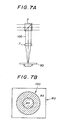
- FIGS.7A and 7B show a portion of an optical pickup device in another embodiment of the present invention.
- the elements which are the same as corresponding elements in FIG.1A are designated by the same reference numerals, and a description thereof will be omitted.
- the reflection beam 100 from the optical disk is reflected to the detecting lens 7 by the beam splitter 3.
- the reflection beam 100 is converted into the converging beam by the detecting lens 7, and the converging beam enters a photodetecting unit 80.
- the photodetecting unit 80 includes a first detecting area "BS" which detects the central portion of the reflection beam 100, and a second detecting area “AS" which detects the peripheral portion of the reflection beam 100.
- the two detecting areas BS and AS are arranged around the center of the photodetecting unit 80, and the first detecting area BS is surrounded by the second detecting area AS.
- a read-data signal SB is generated based on the central portion of the reflection beam 100 detected by the first detecting area BS.
- a read-data signal which is generated based on the peripheral portion of the reflection beam 100 detected by the second detecting area AS is eliminated.
- a sum of a read-data signal SB and a read-data signal SA is generated by the photodetecting unit 80 based on the entire reflection beam detected by the first detecting area BS and the second detecting area AS.
- the positional relation between the photodetecting unit 80 and the detecting lens 7 on the optical axis of the detecting lens 7 is adjusted so that an appropriate light spot on the second detecting area BS is formed by the central portion of the reflection beam 100.
- the aperture unit 9 (not shown in FIG.7A) may or may not be placed on the optical path of the reflection beam directed to the photodetecting unit 80. If the aperture unit 9 is placed, it is possible for the optical pickup device of the present embodiment to more effectively read out data from each of the optical disks 6A and 6B.
- FIGS.8A through 8E show a portion of an optical pickup device in still another embodiment of the present invention.
- the elements in FIGS.8A and 8B are applied to the optical pickup device in FIG.7A.
- FIG.8A shows an optical element 93 which is shaped into a truncated cone
- FIG.8B shows an optical element 95 which is shaped into a truncated prism.
- One of the optical elements 93 and 95 is placed on the optical path between the detecting lens 7 and the photodetecting unit 80 in FIG.7A.
- FIG.8D shows a photodetecting unit 83 which is arranged in combination with the optical element 93 instead of the photodetecting unit 80
- FIG.8E shows a photodetecting unit 85 which is arranged in combination with the optical element 95 instead of the photodetecting unit 80.
- FIG.8C is a side view of the optical element 93 (or 95) and the photodetecting unit 83 (or 85) which are arranged in the optical pickup device.
- Each of the optical elements 93 and 95 separates the reflection beam, directed to the photodetecting unit 83 or 85, into the central portion and the peripheral portion by using refraction, the central portion passing straight and the peripheral portion being refracted to different directions.
- the photodetector unit 83 includes, as shown in FIG.8D, a first detecting area "BS1" which detects the central portion of the reflection beam, and a second detecting area “AS1" which detects the peripheral portion of the reflection beam.
- the two detecting areas BS1 and AS1 are arranged around the center of the photodetecting unit 83, and the first detecting area BS1 is surrounded by the second detecting area AS1.
- a read-data signal SB1 is generated based on the central portion detected by the first detecting area BS1.
- a read-data signal which is generated based on the peripheral portion detected by the second detecting area AS1 is eliminated.
- a sum of a read-data signal SB1 and a read-data signal SA1 is generated by the photodetecting unit 80 based on the entire reflection beam detected by the first detecting area BS1 and the second detecting area AS1.
- the photodetector unit 85 includes, as shown in FIG.8E, a first rectangular detecting area "BS1" which detects the central portion of the reflection beam, and a plurality of second rectangular detecting areas "AS2", “AS3”, “AS4" and "AS5" which detect the peripheral portion of the reflection beam. These areas BS1 and AS2-AS5 are arranged around the center of the photodetecting unit 85, and the area BS1 is surrounded by the areas AS2-AS5.
- a read-data signal SB1 is generated based on the central portion detected by the detecting area BS1.
- a sum of a read-data signal SB1 and read-data signals SA2-SA5 is generated by the photodetecting unit 85 based on the entire reflection beam detected by the detecting area BS1 and the detecting areas AS2-AS5.
- FIGS.9A, 9B and 9C show a portion of an optical pickup device in a further embodiment of the present invention.
- the elements which are the same as corresponding elements in FIG.1A are designated by the same reference numerals, and a description thereof will be omitted.
- the optical pickup device of the present embodiment uses a diffraction unit 97 in FIG.9A instead of the aperture unit 9 in FIG.1A.
- the diffraction unit 97 separates the reflection beam 100, directed to the photodetecting unit, into the central portion and the peripheral portion by using diffraction.
- the diffraction unit 97 includes a transparent area 97A and a diffraction grating 97B, the diffraction grating 97B surrounded by the transparent area 97A.
- the peripheral portion of the reflection beam 100 passes through the transparent area 97A of the diffraction unit 97 to the photodetector unit.
- the center portion of the reflection beam 100 is converted into a diffraction beam by the diffraction grating 97B, the diffraction beam passing in a predetermined direction different from the direction of the peripheral portion.
- a preferred example of the diffraction grating 97B is a hologram diffraction grating or a blaze-type diffraction grating having a nearly 100% diffraction efficiency.
- the optical pickup device of the present embodiment uses a photodetecting unit 87 in FIG.9C instead of the photodiode 8 in FIG.1A.
- the reflection beam 100 from the optical disk is reflected to the diffraction unit 97 by the beam splitter 3.
- the reflection beam 100 is separated into the central portion and the peripheral portion by the diffraction unit 97 by using diffraction, as described above.
- the peripheral portion of the reflection beam from the diffraction unit 97 is converted into the converging beam by the detecting lens 7, and the converging beam enters the photodetecting unit 87 at a first position.
- the diffraction beam (the central portion of the reflection beam) from the diffraction unit 97 is also converted into the converging beam by the detecting lens 7, and the converging beam passing in the predetermined direction enters the photodetecting unit 87 at a second position different from the first position of the above peripheral portion.
- the photodetecting unit 87 has a first detecting area 87A which detects the peripheral portion of the reflection beam, and a second detecting area 87B which detects the central portion of the reflection beam.
- the two detecting areas 87A and 87B of the photodetecting unit 87 are arranged such that they are separate from each other.
- a read-data signal is generated by the photodetecting unit 87 based on the central portion of the reflection beam detected by the second detecting area 87B.
- a read-data signal generated based on the peripheral portion of the reflection beam detected by the first detecting area 87A is eliminated.
- a sum of a first read-data signal and a second read-data signal is generated by the photodetecting unit 87 based on the entire reflection beam detected by the first and second detecting areas 87A and 87B.
- FIGS.10A and 10B show a portion of an optical pickup device in another embodiment of the present invention.
- the elements which are the same as corresponding elements in FIG.1A are designated by the same reference numerals, and a description thereof will be omitted.
- a reflection unit 99 in FIG.10A is used in the optical pickup device instead of the aperture unit 9 in FIG.1A.
- the reflection unit 99 separates the reflection beam 100, directed to the photodetecting unit, into the central portion and the peripheral portion by using reflection.
- the reflection unit 99 includes a transparent area 99A and a reflection mirror 99B, the reflection mirror 99B surrounded by the transparent area 99A.
- the peripheral portion of the reflection beam 100 passes through the transparent area 99A of the reflection unit 99 to a photodetecting unit.
- the center portion of the reflection beam 100 is reflected to another photodetecting unit by the reflection mirror 99B, the reflected beam passing in a predetermined direction different from the direction of the peripheral portion.
- the reflection unit 99 is placed in a 45° slanting condition on the optical path of the reflection beam from the beam splitter 3 and the detecting lens 7.
- a first photodiode 80A and a second photodiode 80B are used in the optical pickup device of the present embodiment instead of the photodiode 8 in FIG.1A.
- a second detecting lens 7B is placed on an optical path of the reflected beam from the reflection unit 99 to the second photodiode 80B, in addition to the detecting lens 7.
- the reflection beam 100 from the optical disk is reflected to the reflection unit 99 by the beam splitter 3. As described above, the reflection beam 100 is separated into the central portion and the peripheral portion by the reflection unit 99 by using reflection.
- the peripheral portion of the reflection beam from the transparent area 99A of the reflection unit 99 is converted into a converging beam by the detecting lens 7, and the converging beam enters the first photodiode 80A.
- the reflected beam (the central portion of the reflection beam) from the reflection mirror 99B is converted into a converging beam by the second detecting lens 7B, and the converging beam enters the second photodiode 80B.
- the converging beam (the central portion of the reflection beam) from the second detecting lens 7B is detected by the second photodiode 80B, and a read-data signal is generated by the second photodiode 80B based on the central portion of the reflection beam.
- the generation of a read-data signal based on the peripheral portion of the reflection beam by the second photodiode 80B is inhibited.
- the converging beam (the peripheral portion of the reflection beam) from the detecting lens 7 is detected by the first photodiode 80A, and a sum of a first read-data signal and a second read-data signal is generated by the first photodiode 80A and the second photodiode 80B based on the entire reflection beam.
- the detecting lens 7 and the second detecting lens 7B are used to convert the reflection beam into a converting beam so that the converting beam correctly enters the photodetecting unit.
- the detecting lens 7 and/or the second detecting lens 7B must be included in order to correctly detect the reflection beam from the optical disk.
- FIGS.11A and 11B show an optical pickup device to which a further embodiment of the present invention is applied.
- the elements which are the same as corresponding elements in FIG.1A are designated by the same reference numerals, and a description thereof will be omitted.
- a light emission/ detection unit 21 includes a laser diode 21A and a photodiode 21B.
- the laser diode 21A emits an emission beam which is directed to an optical disk.
- the photodiode 21B detects a reflection beam which is reflected off from the optical disk, and generates a read-data signal based on the reflection beam.
- the laser diode 21A and the photodiode 21B are packaged in a single unit.
- the light emission/ detection unit 21 has a window portion to which a cover glass 21C is attached.
- the emission beam and the reflection beam pass through the cover glass 21C.
- the emission beam (which is a linearly polarized light) from the light emission/detection unit 21 passes through a polarization hologram 22 to a quarter-wave plate 23.
- the emission beam is converted into a circularly polarized light by the quarter-wave plate 23.
- the circularly polarized light from the quarter-wave plate 23 is deflected to the objective lens 5 by the deflection prism 4.
- the deflected beam from the deflection prism 4 is converted into a converging beam by the objective lens 5.
- the converging beam from the objective lens 5 passes through the transparent layer 62 of the optical disk 6A (or 6B), and a light spot on the recording surface 60 (or 61) of the optical disk is formed.
- the optical characteristics of the objective lens 5 in FIG.11B are preset based on the thickness (0.6 mm) of the transparent layer 62 of the optical disk 6A. Therefore, when the optical disk 6A is accessed, the light spot on the recording surface 60 of the optical disk 6A is correctly formed.
- a reflection beam from the optical disk passes through the objective lens 5, and it is deflected by the deflection prism 4 to the quarter-wave plate 23.
- the reflection beam (which is a circularly polarized light) from the deflection prism 4 is converted into a linearly polarized light by the quarter-wave plate 23.
- the linearly polarized light from the quarter-wave plate 23 enters the polarization hologram 22.
- the linearly polarized light from the quarter-wave plate 23 is deflected to the photodiode 21B of the light emission/detection unit 21 by the polarization hologram 22.
- the polarized light of the reflection beam when entering the polarization hologram 22 has a plane of polarization shifted 90° from a plane of polarization of the linearly polarized light of the emission beam from the laser diode 21A. Therefore, the polarized light is deflected to the photodiode 21B by the polarization hologram 22.
- FIG.12 shows the polarization hologram 22 of the optical pickup device in FIGS.11A and 11B.
- the polarization hologram 22 has a hologram area 22A which deflects the central portion of the reflection beam 100 to the photodiode 21B by using polarization.
- the central portion of the reflection beam 100 from the hologram area 22A enters the photodiode 21B.
- the peripheral portion of the reflection beam 100 passes through a peripheral area of the polarization hologram 22, other than the hologram area 22A, without deflection.
- the peripheral portion of the reflection beam 100 from the peripheral area of the polarization hologram 22 does not enter the photodiode 21B.
- the optical characteristics of the objective lens 5 are preset based on the thickness (0.6 mm) of the transparent layer 62 of the optical disk 6A, and the light spot on the recording surface 60 of the optical disk 6A is correctly formed. Therefore, when the disk 6A is accessed, the polarization hologram 22 converts the reflection beam 100 directed to the photodiode 21B such that the reflection beam 100 is allowed to enter the photodiode 21B by using the above polarization.
- the polarization hologram 22 converts the reflection beam directed to the photodiode 21B such that the central portion of the reflection beam 100 is allowed to enter the photodiode 8 by using the above polarization, and the peripheral portion of the reflection beam 100 is inhibited from entering the photodiode 8.
- the detection of a focus error signal and a tracking error signal is performed separately from the read-data signal generated by the photodiode 8 based on the reflection beam from the optical disk.
- a polarization hologram 220 and a photodetecting unit 210B it is possible to generate a focus error signal and a tracking error signal as well as a read-data signal based on the reflection beam from the optical disk with no need for the focus error detecting unit or the tracking error detecting unit.
- FIGS.13A and 13B show another polarization hologram 220 and another photodetecting unit 210B for use in the optical pickup device in FIG.11B.
- the polarization hologram 220 has a hologram area 220A which deflects the central portion of the reflection beam 100 to the photodiode 21B.
- the hologram area 220A is divided into three holograms 20A, 20B and 20C, the hologram 20A located at an upper half portion of the hologram area 220A, and the holograms 20B and 20C located at lower quarter portions of the hologram area 220A.
- the photodetecting unit 210B is divided into four light detecting areas "a" through “d", the light detecting areas located as shown in FIG.13B.
- an upper half of the central portion of the reflection beam from the optical disk is deflected by the hologram 20A of the polarization hologram 220 to the photodetecting unit 210B, and the deflected reflection beam from the hologram 20A enters around the boundary between the light detecting areas "a" and "b" of the photodetecting unit 210B.
- Lower quarters of the central portion of the reflection beam 100 from the optical disk are deflected by the holograms 20B and 20C to the photodetecting unit 210B, and the deflected reflection beams from the holograms 20B and 20C enter the light detecting areas "c" and "d” of the photodetecting unit 210B, respectively.
- a focus error signal can be obtained by generating the difference "Sa - Sb" between the first and second signals Sa and Sb by utilizing a known knife-edge method. Since the light detecting areas "c" and “d” output a third signal Sc and a fourth signal Sd based on the reflection beam from the optical disk, a tracking error signal can be obtained by generating the difference "Sc - Sd” between the third and fourth signals Sc and Sd by utilizing a known push-pull method. Further, in the present embodiment, a read-data signal can be obtained by generating the sum "Sa + Sb + Sc + Sd" of the signals Sa, Sb, Sc and Sd for each of the optical disks 6A and 6B.
- the generation of the read-data signal based on the reflection beam is suitably performed by using the polarization hologram 220 and the photodetecting unit 210B.
- the optical disk 6A with the smaller transparent layer thickness (0.6 mm) is accessed, the amplitude of the read-data signal generated by the photodetecting unit 210B is reduced due to the use of the polarization hologram 220.
- a waveform equalizer circuit may be added to the optical pickup device of the present embodiment.
- the amplitude of the signal output by the photodetecting unit 210B can be electrically corrected by the waveform equalizer circuit.
- FIG.14 shows a further polarization hologram 221 and a further photodetecting unit 211B for use in the optical pickup device in FIG.11B.
- the elements of the optical pickup device which are the same as corresponding elements in FIG.11B are not shown in FIG.14 and a description thereof will be omitted for the sake of convenience.
- the polarization hologram 221 has a hologram area 221A which deflects the central portion of the reflection beam 100 to the photodetecting unit 211B, and a hologram area 221B which deflects the peripheral portion of the reflection beam to the photodetecting unit 211B.
- the hologram area 221A is divided into three holograms 20A, 20B and 20C similarly to the embodiment in FIGS.13A and 13B.
- the photodetecting unit 211B is divided into five light detecting areas "a'" through "e'".
- an upper half of the central portion of the reflection beam from the optical disk is deflected by the hologram 20A to the photodetecting unit 211B, and the deflected reflection beam from the hologram 20A enters around the boundary between the light detecting areas "a'" and "b'” of the photodetecting unit 211B.
- Lower quarters of the central portion of the reflection beam from the optical disk are deflected by the holograms 20B and 20C to the photodetecting unit 210B, and the deflected reflection beams from the holograms 20B and 20C enter the light detecting areas "c'" and "d'" of the photodetecting unit 211B, respectively.
- the peripheral portion of the reflection beam from the optical disk is deflected by the hologram area 221B to the photodetecting unit 211B, and the deflected reflection beam enters the light detecting area "e'" of the photodetecting unit 211B.
- a focus error signal can be obtained by generating the difference "Sa - Sb" between the signals Sa and Sb by utilizing the known knife-edge method.
- the light detecting areas "c'” and “d'” output a third signal Sc and a fourth signal Sd based on the reflection beam from the optical disk, a tracking error signal can be obtained by generating the difference "Sc - Sd” between the signals Sc and Sd by utilizing the known push-pull method.
- the light detecting area "e'” outputs a fifth signal Se based on the periperal portion of the reflection beam from the optical disk.
- a read-data signal when the optical disk 6B is accessed, a read-data signal can be obtained by generating the sum "Sa + Sb + Sc + Sd" of the signals Sa, Sb, Sc and Sd, and when the optical disk 6A is accessed, a read-data signal can be obtained by generating the sum "Sa + Sb + Sc + Sd + Se” of the signals Sa, Sb, Sc, Sd and Se.
- the generation of the read-data signal based on the reflection beam is suitably performed by using the polarization hologram 221 and the photodetecting unit 211B.
- FIG.15 shows a variation of the optical pickup device in FIG.11B.
- the elements which are the same as corresponding elements in FIG.11B are designated by the same reference numerals, and a description thereof will be omitted.
- the collimator lens 2 is provided on an optical path of the emission beam from the light source (the laser diode 21A) to the objective lens 5.
- the collimator lens 2 converts the emission beam from the light source 21A into a parallel beam, the parallel beam passing through the polarization hologram 22 to the quarter-wave plate 23.
- the polarization hologram 22 is placed between the collimator lens 2 and the objective lens 5. Also, the quarter-wave plate 23 is placed between the polarization hologram 22 and the objective lens 5.
- no collimator lens is provided on the optical path of the emission beam. If a distance between the laser diode 21A and the photodiode 21B in the direction B perpendicular to the optical path is about 1 mm and a distance between the polarization hologram 22 and the laser diode 21A in the direction A parallel to the optical path is about 5 mm, a deflection angle required for the polarization hologram 22 to make the polarized light of the center portion of the reflection beam correctly converge on the photodiode 21B is about 11.5 degrees. The deflection angle in this case is relatively great, and it is difficult that the size of the optical pickup device be reduced.
- the collimator lens 2 is provided, and this allows the size of the optical pickup device of the present embodiment to be reduced. If a focal length of the collimator lens 2 is about 16 mm, the distance between the laser diode 21A and the photodiode 21B in the direction B is about 1 mm and the distance between the polarization hologram 22 and the laser diode 21A in the direction A is about 5 mm, the deflection angle required for the polarization hologram 22 to make the polarized light of the center portion of the reflection beam correctly converge on the photodiode 21B is about 3.6 degrees which is rather smaller than the deflection angle of the embodiment in FIG.11B. Therefore, it is possible for the present embodiment to considerably reduce the size of the optical pickup device.
- FIG.16 shows another variation of the optical pickup device in FIG.11B.
- the elements which are the same as corresponding elements in FIG.11B are designated by the same reference numerals, and a description thereof will be omitted.
- a polarization hologram 22A is attached to the window portion of the light emission/detection unit 21 by using adhesive agent so that the laser diode 21A, the photodiode 21B, and the polarization hologram 22A are integrally formed with the light emission/detection unit 21.
- the collimator lens 2 is provided on the optical path of the emission beam from the laser diode 21A to the objective lens 5. The collimator lens 2 converts the emission beam from the light source 21A into a parallel beam, the parallel beam entering the quarter-wave plate 23.
- the laser diode 21A, the photodiode 21B, and the polarization hologram 22A are integrally formed with the light emission/detection unit 21, it is possible for the present embodiment to further reduce the size of the optical pickup device.
- FIG.17 shows a further light emission/ detection unit 21 for use in the optical pickup device in FIGS.11B.
- the elements which are the same as corresponding elements in FIG.11A are designated by the same reference numerals, and a description thereof will be omitted.
- the light emission/ detection unit 21 includes the laser diode 21A, the photodiode 21B, the polarization hologram 22A, and a quarter-wave plate 23A which are arranged within a single unit.
- the polarization hologram 22A is attached to the window portion of the light emission/detection unit 21 by using adhesive agent.
- the quarter-wave plate 23A is attached to the polarization hologram 22A by using adhesive agent.
- the optical pickup device of the present embodiment uses a simple structure which is useful to reduce the cost or allow an efficient manufacture of the optical pickup device.
- the polarization hologram 22 (or 220, 221) includes the hologram 22A (or 220A, 221A) which is shaped into a circle, the circle having a center on the optical path of the reflection beam.
- the hologram 22A (or 220A, 221A) of the present invention is not limited to these embodiments.
- a polarization hologram having a hologram shaped into an ellipse, the ellipse having a center on the optical path of the reflection beam, may be suitably used by the optical pickup device of the present invention.
- FIG.19 shows a further polarization hologram 22B for use in the optical pickup device in FIG.11B.
- the direction parallel to a track of the optical disk is indicated by an arrow "A”
- the direction perpendicular to the direction of the track of the optical disk is indicated by an arrow "B”.
- the polarization hologram 22B has a rectangular hologram 22B1 which detects the central portion of the reflection beam 100 from the quarter-wave plate 23.
- the rectangular hologram 22B1 extends in the direction "A" parallel to a track of the optical disk.
- the polarization hologram 22B in FIG.19 is used instead in the optical pickup device in FIG.11B.
- the rectangular hologram 22B1 deflects the center portion of the reflection beam to the photodetecting unit 21B when each of the optical disks 6A and 6B is accessed.
- the rectangular hologram 22B1 has an advantageous feature which is the same as that of the aperture unit 91 shown in FIG.5. For details of the advantageous feature of the aperture unit 91, see the above description thereof with reference to FIGS.6A, 6B and 6C.
Landscapes
- Physics & Mathematics (AREA)
- Optics & Photonics (AREA)
- Optical Head (AREA)
Claims (19)
- Optische Abtastvorrichtung zum Zugreifen sowohl auf eine erste optische Platte (6A), die eine transparente Schicht mit einer ersten Dicke aufweist, als auch auf eine zweite optische Platte (6B), die eine transparente Schicht mit einer zweiten, größeren Dicke aufweist, umfassend:gekennzeichnet durch ein Strahlwandlungsmittel (90, 91, 93, 95, 97, 99, 22 und 23, 22A und 23A), das nur auf den Reflexionsstrahl von der optischen Platte und nicht auf den abgestrahlten Strahl von der Lichtquelle einwirkt, der auf die optische Platte gerichtet ist, um einen Reflexionsstrahl, der auf die Fotodetektionseinrichtung gerichtet bzw. abgebildet ist, so zu wandeln, dass ein peripherer Teil des Reflexionsstrahls auf die Fotodetektionseinrichtung (8) gelangen kann, wenn auf die erste optische Platte zugegriffen wird, und dass der periphere Teil des Reflexionsstrahls nicht auf die Fotodetektionseinrichtung (8) gelangen kann, wenn auf die zweite optische Platte zugegriffen wird, wobeieine Lichtquelle (1), um einen Laserstrahl zu einer optischen Platte abzustrahlen;ein Objektiv bzw. eine Objektivlinse (5), um den abgestrahlten Strahl von der Lichtquelle in einen konvergierenden Strahl zu wandeln, wobei der konvergierende Strahl eine transparente Schicht der optischen Platte durchquert und auf einer Aufzeichnungsoberfläche (60; 61) der optischen Platte einen Lichtfleck bildet, wobei das Objektiv bzw. die Objektivlinse optische Eigenschaften aufweist, die in Abhängigkeit von der ersten Dicke der ersten optischen Platte voreingestellt sind; undeine Fotodetektionseinrichtung (8), um ein Lese-Datensignal auf der Grundlage eines Reflexionsstrahls von der optischen Platte zu erzeugen;(a) das Strahlwandlungsmittel eine Blendeneinheit (90, 91) ist, die in eine Lichtblockierstellung und in eine Lichtdurchlassstellung einstellbar ist, und die eine von einer Kreisform abweichende Form, insbesondere eine elliptische oder rechteckförmige Form, aufweist; oder(b) das Strahlwandlungsmittel (93, 95) den Reflexionsstrahl, der auf die Fotodetektionseinrichtung gerichtet ist, in den zentralen Teil und den peripheren Teil auf Grund einer Lichtbrechung trennt; oder(c) das Strahlwandlungsmittel (97) den Reflexionsstrahl, der auf die Fotodetektionseinrichtung gerichtet ist, in den zentralen Teil und den peripheren Teil auf Grund einer Lichtbeugung trennt; oder(d) das Strahlwandlungsmittel (99) den Reflexionsstrahl, der auf die Fotodetektionseinrichtung gerichtet ist, in den zentralen Teil und den peripheren Teil auf Grund einer Reflexion trennt; oder(e) das Strahlwandlungsmittel ein Lambda-Viertel-Plättchen (23) und ein Polarisationshologramm bzw. polarisierendes Hologramm (22) umfasst.
- Optische Abtastvorrichtung nach Anspruch 1, dadurch gekennzeichnet, dass die optische Abtastvorrichtung weiterhin umfasst:Einstellmittel (10), um das Strahlwandlungsmittel in eine erste Stellung, in welcher der zentrale Teil und der periphere Teil des Reflexionsstrahls auf die Fotodetektionseinrichtung (8) gelangen kann, oder in eine zweite Stellung, in welcher der periphere Teil des Reflexionsstrahls nicht auf die Fotodetektionseinrichtung gelangen kann und nur der zentrale Teil des Reflexionsstrahls auf die Fotodetektionseinrichtung gelangen kann, einzustellen.
- Optische Abtastvorrichtung nach Anspruch 1, dadurch gekennzeichnet, dass die Blendeneinheit (9, 91) eine Lichtblockierscheibe mit einer Öffnung umfasst, wobei die Lichtblockierscheibe auf einem optischen Pfad bzw. Strahlengang des auf die Fotodetektionseinrichtung (8) gerichteten Reflexionsstrahls angeordnet ist, wenn auf die zweite optische Platte zugegriffen wird, so dass die Lichtblockierscheibe verhindert, dass der periphere Teil des Reflexionsstrahls auf die Fotodetektionseinrichtung gelangt, und die Öffnung nur zulässt, dass der zentrale Teil des Reflexionsstrahls auf die Fotodetektionseinrichtung gelangt.
- Optische Abtastvorrichtung nach Anspruch 1, dadurch gekennzeichnet, dass die Blendeneinheit (9, 91) einen Flüssigkristallverschluss (90) mit einer Öffnung umfasst, wobei der Flüssigkristallverschluss elektrisch in eine erste Stellung, in welcher der zentrale Teil und der periphere Teil des Reflexionsstrahls durch den Verschluss zu der Fotodetektionseinrichtung (8) gelangen kann, oder in eine zweite Stellung eingestellt wird, in welcher der zentrale Teil des Reflexionsstrahls nicht auf die Fotodetektionseinrichtung (8) gelangen kann und nur der zentrale Teil des Reflexionsstrahls durch die Öffnung hindurch zu der Fotodetektionseinrichtung (8) gelangen kann.
- Optische Abtastvorrichtung nach Anspruch 1, dadurch gekennzeichnet, dass die Blendeneinheit (9, 91) eine Lichtblockierscheibe mit einer Öffnung umfasst, welche die Form eines Kreises oder einer Ellipse aufweist.
- Optische Abtastvorrichtung nach Anspruch 1, dadurch gekennzeichnet, dass die Blendeneinheit (91) ein Paar von Lichtblockierscheiben (91B, 91C) und eine rechteckige Öffnung (91A) zwischen den Lichtblockierscheiben umfasst, wobei die rechteckige Öffnung sich in einer Richtung parallel zu einer Spur der optischen Platte (6A, 6B) erstreckt.
- Optische Abtastvorrichtung nach Anspruch 1, dadurch gekennzeichnet, dass die Fotodetektionseinrichtung (80) einen ersten Detektionsbereich und einen zweiten Detektionsbereich aufweist, die selektiv ein Lese-Datensignal auf der Grundlage des Reflexionsstrahls von der optischen Platte erzeugen, so dass dann, wenn auf die zweite optische Platte zugegriffen wird, der erste Detektionsbereich ein Lese-Datensignal auf der Grundlage nur des zentralen Teils erzeugt, und dann, wenn auf die zweite optische Platte zugegriffen wird, der erste Detektionsbereich und der zweite Detektionsbereich ein Lese-Datensignal auf der Grundlage des gesamten Reflexionsstrahls erzeugen.
- Optische Abtastvorrichtung nach Anspruch 7, dadurch gekennzeichnet, dass der erste Detektionsbereich ausgelegt ist, um den zentralen Teil des Reflexionsstrahls zu detektieren, und dass der zweite Detektionsbereich ausgelegt ist, um den peripheren Teil des Reflexionsstrahls zu detektieren, wobei der erste Detektionsbereich von dem zweiten Detektionsbereich umgeben ist.
- Optische Abtastvorrichtung nach Anspruch 7, dadurch gekennzeichnet, dass das Strahlwandlungsmittel den Reflexionsstrahl, der auf die Fotodetektionseinrichtung gerichtet ist, in den zentralen Teil und in den peripheren Teil unter Verwendung einer Lichtbrechung auftrennt, wobei das Strahlwandlungsmittel ein optisches Element (93, 95) umfasst, das kegelstumpfförmig oder wie eine abgeschnittene Pyramide geformt ist.
- Optische Abtastvorrichtung nach Anspruch 7, dadurch gekennzeichnet, dass das Strahlwandlungsmittel (97) den Reflexionsstrahl, der auf die Fotodetektionseinrichtung gerichtet ist, in den zentralen Teil und in den peripheren Teil auf Grund einer Lichtbeugung auftrennt, wobei das Strahlwandlungsmittel ein Beugungsgitter (97B) umfasst, das von einem transparenten Bereich (97A) umgeben ist.
- Optische Abtastvorrichtung nach Anspruch 7, dadurch gekennzeichnet, dass das Strahlwandlungsmittel (99) den Reflexionsstrahl, der auf die Fotodetektionseinrichtung gerichtet ist, in den zentralen Teil und den peripheren Teil auf Grund einer Reflexion auftrennt, wobei das Strahlwandlungsmittel einen Reflexionsspiegel (99B) umfasst, der von einem transparenten Bereich (99A) umgeben ist.
- Optische Abtastvorrichtung nach Anspruch 1, dadurch gekennzeichnet, dass das Strahlwandlungsmittel ein Lambda-Viertel-Plättchen (23) und ein Polarisationshologramm (22) umfasst, wobei das Polarisationshologramm auf einem optischen Pfad bzw. Strahlengang des von der Lichtquelle zu dem Lambda-Viertel-Plättchen abgestrahlten Strahls angeordnet ist, wobei das Polarisationshologramm den von der Lichtquelle zu der optischen Platte abgestrahlten Strahl ohne Strahlablenkung durchlässt und ein polarisiertes Licht des zentralen Teils des Reflexionsstrahls von dem Lambda-Viertel-Plättchen zu der Fotodetektionseinrichtung ab- bzw. umlenkt.
- Optische Abtastvorrichtung nach Anspruch 12, dadurch gekennzeichnet, dass die Fotodetektionseinrichtung (22, 220, 221) einen ersten Detektionsbereich und einen zweiten Detektionsbereich aufweist, die selektiv ein Lese-Datensignal auf der Grundlage des Reflexionsstrahls von der optischen Platte erzeugt, so dass dann, wenn auf die zweite optische Platte zugegriffen wird, der erste Detektionsbereich den zentralen Teil des Reflexionsstrahls detektiert, um ein Lese-Datensignal auf der Grundlage des zentralen Teils zu erzeugen, und dann, wenn auf die erste optische Platte zugegriffen wird, der erste Detektionsbereich und der zweite Detektionsbereich den zentralen Teil und den peripheren Teil des Reflexionsstrahls detektieren, um eine Summe der ersten und zweiten Lese-Datensignale auf der Grundlage des gesamten Reflexionsstrahls zu erzeugen.
- Optische Abtastvorrichtung nach Anspruch 12, dadurch gekennzeichnet, dass die optische Abtastvorrichtung weiterhin umfasst:wobei das Polarisationshologramm (22) zwischen der Kollimatorlinse und der Objektivlinse bzw. dem Objektiv angeordnet ist.eine Kollimatorlinse (2), die auf einem optischen Pfad bzw. Strahlgang des von der Lichtquelle zu der Objektivlinse bzw. dem Objektiv abgestrahlten Strahls angeordnet ist, wobei die Kollimatorlinse den von der Lichtquelle abgestrahlten Strahl in einen parallelen Strahl wandelt, welcher parallele Strahl das Polarisationshologramm zu dem Lambda-Viertel-Plättchen hin durchquert,
- Optische Abtastvorrichtung nach Anspruch 12, dadurch gekennzeichnet, dass das Polarisationshologramm (22A) an einem Fensterabschnitt (21 C) einer Lichtemissions-/-detektionseinheit (21) angebracht ist und dass die Lichtquelle (21A), das Fotodetektionsmittel (21B) und das Polarisationshologramm (22A) integral bzw. einstückig mit der Lichtemissions-/-detektionseinheit ausgebildet sind.
- Optische Abtastvorrichtung nach Anspruch 15, dadurch gekennzeichnet, dass das Lambda-Viertel-Plättchen (23A) außerdem an dem Polarisationshologramm (22A) angebracht ist, so dass die Lichtquelle (21A), die Fotodetektionseinrichtung (21B), das Polarisationshologramm (22A) und das Lambda-Viertel-Plättchen (23A) integral bzw. einstückig mit der Lichtemissions-/-detektionseinheit ausgebildet sind.
- Optische Abtastvorrichtung nach Anspruch 12, dadurch gekennzeichnet, dass das Polarisationshologramm (22B) ein rechteckiges Hologramm (22B1) umfasst, das den von der Lichtquelle zu der optischen Platte abgestrahlten Strahl durchlässt und ein polarisiertes Licht des zentralen Teils des Reflexionsstrahls von dem Lambda-Viertel-Plättchen zu der Fotodetektionseinrichtung ab- bzw. umlenkt, wobei das rechteckige Hologramm sich in einer Richtung parallel zu einer Spur der optischen Platte erstreckt.
- Optische Abtastvorrichtung nach Anspruch 12, dadurch gekennzeichnet, dass die Fotodetektionseinrichtung (210B) in eine Mehrzahl von Lichtdetektionsbereichen unterteilt ist, die den zentralen Teil des Reflexionsstrahls von dem Polarisationshologramm detektieren, und dass die Fotodetektionseinrichtung (210B) und das Polarisationshologramm (220) so ausgelegt sind, dass ein Fokusfehlersignal und ein Spurfehlersignal durch Erzeugen eines Differenzsignals zwischen Signalen, die von der Mehrzahl von Lichtdetektionsbereichen auf der Grundlage des zentralen Teils des Reflexionsstrahls erzeugt werden, erhalten werden.
- Optische Abtastvorrichtung nach Anspruch 12, dadurch gekennzeichnet, dass die Lichtquelle (21A) und die Fotodetektionseinrichtung (21B) in einer einzigen Einheit (21) angeordnet sind.
Applications Claiming Priority (6)
| Application Number | Priority Date | Filing Date | Title |
|---|---|---|---|
| JP29839895A JP3236203B2 (ja) | 1995-11-16 | 1995-11-16 | 光ピックアップ装置 |
| JP29839895 | 1995-11-16 | ||
| JP298398/95 | 1995-11-16 | ||
| JP4609/96 | 1996-01-16 | ||
| JP00460996A JP3216691B2 (ja) | 1996-01-16 | 1996-01-16 | 光ピックアップ装置 |
| JP460996 | 1996-01-16 |
Publications (3)
| Publication Number | Publication Date |
|---|---|
| EP0774751A2 EP0774751A2 (de) | 1997-05-21 |
| EP0774751A3 EP0774751A3 (de) | 1998-05-20 |
| EP0774751B1 true EP0774751B1 (de) | 2004-01-07 |
Family
ID=26338413
Family Applications (1)
| Application Number | Title | Priority Date | Filing Date |
|---|---|---|---|
| EP96118267A Expired - Lifetime EP0774751B1 (de) | 1995-11-16 | 1996-11-14 | Optische Abtastvorrichtung zur Wiedergabe von unterschiedlichen optischen Platten |
Country Status (3)
| Country | Link |
|---|---|
| US (2) | US5717678A (de) |
| EP (1) | EP0774751B1 (de) |
| DE (1) | DE69631281T2 (de) |
Families Citing this family (8)
| Publication number | Priority date | Publication date | Assignee | Title |
|---|---|---|---|---|
| US5717678A (en) * | 1995-11-16 | 1998-02-10 | Ricoh Company, Ltd. | Optical pickup device for accessing each of optical disks of different types |
| US20010050892A1 (en) * | 1997-07-11 | 2001-12-13 | Yoshitaka Takahashi | Optical disk apparatus compatible with different types of mediums |
| US6195315B1 (en) * | 1997-07-11 | 2001-02-27 | Ricoh Company, Ltd. | Optical disk apparatus compatible with different types of mediums |
| JPH11134732A (ja) * | 1997-08-29 | 1999-05-21 | Canon Inc | 情報記録再生方法 |
| EP1057175B1 (de) * | 1998-12-29 | 2008-07-23 | Koninklijke Philips Electronics N.V. | Optische abtastvorrichtung für zwei verschiedene arten von aufzeichnungsträgern |
| ATE363122T1 (de) | 1999-01-22 | 2007-06-15 | Konica Minolta Opto Inc | Optische abtastvorrichtung zur informationsaufzeichnung und informationswiedergabe |
| JP4085812B2 (ja) * | 2000-09-06 | 2008-05-14 | 株式会社日立製作所 | 光ヘッドおよび光ディスク装置 |
| KR20070116875A (ko) * | 2005-03-11 | 2007-12-11 | 코닌클리케 필립스 일렉트로닉스 엔.브이. | 광학주사장치 |
Citations (1)
| Publication number | Priority date | Publication date | Assignee | Title |
|---|---|---|---|---|
| EP0390445A2 (de) * | 1989-03-27 | 1990-10-03 | Matsushita Electric Industrial Co., Ltd. | Optischer Abtastkopf |
Family Cites Families (11)
| Publication number | Priority date | Publication date | Assignee | Title |
|---|---|---|---|---|
| JPH0354740A (ja) * | 1989-07-24 | 1991-03-08 | Matsushita Electric Ind Co Ltd | 光学情報記録部材および光学情報記録再生装置 |
| US5235581A (en) * | 1990-08-09 | 1993-08-10 | Matsushita Electric Industrial Co., Ltd. | Optical recording/reproducing apparatus for optical disks with various disk substrate thicknesses |
| US5206852A (en) * | 1991-06-29 | 1993-04-27 | Samsung Electronics Co., Ltd. | High-density recording optical head |
| JPH0777031B2 (ja) * | 1991-10-16 | 1995-08-16 | インターナショナル・ビジネス・マシーンズ・コーポレイション | 収差補償装置 |
| US5281797A (en) * | 1991-12-26 | 1994-01-25 | Hitachi, Ltd. | Short wavelength optical disk head having a changeable aperture |
| JP2532818B2 (ja) * | 1993-02-01 | 1996-09-11 | 松下電器産業株式会社 | 対物レンズおよび光ヘッド装置 |
| JP2993391B2 (ja) * | 1995-03-03 | 1999-12-20 | 日本ビクター株式会社 | 光ピックアップ |
| DE69608750T2 (de) * | 1995-03-15 | 2001-02-15 | Koninklijke Philips Electronics N.V., Eindhoven | Vorrichtung zum optischen abtasten eines auzeichnungsmediums |
| KR960038794A (ko) * | 1995-04-14 | 1996-11-21 | 사또오 후미오 | 광학적 정보 재생 장치 |
| US5621717A (en) * | 1995-06-07 | 1997-04-15 | International Business Machines Corporation | Reading optical disks having substrates with diverse axial thicknesses |
| US5717678A (en) * | 1995-11-16 | 1998-02-10 | Ricoh Company, Ltd. | Optical pickup device for accessing each of optical disks of different types |
-
1996
- 1996-11-12 US US08/745,421 patent/US5717678A/en not_active Expired - Lifetime
- 1996-11-14 EP EP96118267A patent/EP0774751B1/de not_active Expired - Lifetime
- 1996-11-14 DE DE69631281T patent/DE69631281T2/de not_active Expired - Lifetime
-
1997
- 1997-10-07 US US08/946,592 patent/US5894466A/en not_active Expired - Lifetime
Patent Citations (1)
| Publication number | Priority date | Publication date | Assignee | Title |
|---|---|---|---|---|
| EP0390445A2 (de) * | 1989-03-27 | 1990-10-03 | Matsushita Electric Industrial Co., Ltd. | Optischer Abtastkopf |
Also Published As
| Publication number | Publication date |
|---|---|
| DE69631281D1 (de) | 2004-02-12 |
| EP0774751A3 (de) | 1998-05-20 |
| EP0774751A2 (de) | 1997-05-21 |
| US5717678A (en) | 1998-02-10 |
| US5894466A (en) | 1999-04-13 |
| DE69631281T2 (de) | 2004-11-25 |
Similar Documents
| Publication | Publication Date | Title |
|---|---|---|
| KR100269105B1 (ko) | 두께가다른디스크의호환이가능한기록재생용광픽업 | |
| US4924082A (en) | Optical scanning device, mirror objective suitable for use in said device and optical write and/or read apparatus provided with said device | |
| US4771411A (en) | Device for scanning a radiation-reflecting information surface with optical radiation | |
| US7426169B2 (en) | Optical pickup apparatus and optical pickup method | |
| EP0749119A2 (de) | Optisches Abtastgerät | |
| US4940890A (en) | Optical scanning device, mirror objective suitable for use in said device and optical write and/or read apparatus provided with said device | |
| EP0774751B1 (de) | Optische Abtastvorrichtung zur Wiedergabe von unterschiedlichen optischen Platten | |
| US6400666B1 (en) | Optical pickup device | |
| US5745304A (en) | Integrated optical pickup system capable of reading optical disks of different thickness | |
| EP0805440A1 (de) | Objektivlinsenvorrichtung und optische Abtastvorrichtung mit derselben | |
| EP0612064B1 (de) | Optische Abtastvorrichtung | |
| KR100213270B1 (ko) | 양면 디스크용 광 픽업 | |
| US5293372A (en) | Apparatus for optically recording and reproducing information from an optical recording medium | |
| JPH06302011A (ja) | 光学式走査装置 | |
| US5856961A (en) | Laser detector grating unit (LDGU) for producing focus error, a push-pull tracking error, and differential phase tracking error signals | |
| JP3236203B2 (ja) | 光ピックアップ装置 | |
| US20070247984A1 (en) | Optical Record Carrier and Optical Scanning Device | |
| EP1170737A2 (de) | Kompatibles optisches Abtastgerät mit einer einzelnen Lichtquelle | |
| KR100480638B1 (ko) | 광픽업장치 | |
| JP2506972B2 (ja) | 光ピックアップ装置 | |
| JPH05151593A (ja) | 光ピツクアツプ | |
| KR0181815B1 (ko) | 듀얼 포커스 광 픽-업장치 | |
| KR930009680B1 (ko) | 광기록 재생장치의 주사방법 및 장치 | |
| KR100644588B1 (ko) | 고밀도 기록 재생 가능한 광픽업장치 | |
| KR100343159B1 (ko) | 광픽업에서회절격자를이용한에러신호검출장치 |
Legal Events
| Date | Code | Title | Description |
|---|---|---|---|
| PUAI | Public reference made under article 153(3) epc to a published international application that has entered the european phase |
Free format text: ORIGINAL CODE: 0009012 |
|
| 17P | Request for examination filed |
Effective date: 19961114 |
|
| AK | Designated contracting states |
Kind code of ref document: A2 Designated state(s): DE FR |
|
| PUAL | Search report despatched |
Free format text: ORIGINAL CODE: 0009013 |
|
| AK | Designated contracting states |
Kind code of ref document: A3 Designated state(s): DE FR |
|
| 17Q | First examination report despatched |
Effective date: 20010615 |
|
| GRAH | Despatch of communication of intention to grant a patent |
Free format text: ORIGINAL CODE: EPIDOS IGRA |
|
| GRAS | Grant fee paid |
Free format text: ORIGINAL CODE: EPIDOSNIGR3 |
|
| GRAA | (expected) grant |
Free format text: ORIGINAL CODE: 0009210 |
|
| AK | Designated contracting states |
Kind code of ref document: B1 Designated state(s): DE FR |
|
| REF | Corresponds to: |
Ref document number: 69631281 Country of ref document: DE Date of ref document: 20040212 Kind code of ref document: P |
|
| ET | Fr: translation filed | ||
| PLBE | No opposition filed within time limit |
Free format text: ORIGINAL CODE: 0009261 |
|
| STAA | Information on the status of an ep patent application or granted ep patent |
Free format text: STATUS: NO OPPOSITION FILED WITHIN TIME LIMIT |
|
| 26N | No opposition filed |
Effective date: 20041008 |
|
| PGFP | Annual fee paid to national office [announced via postgrant information from national office to epo] |
Ref country code: DE Payment date: 20101119 Year of fee payment: 15 |
|
| PGFP | Annual fee paid to national office [announced via postgrant information from national office to epo] |
Ref country code: FR Payment date: 20111130 Year of fee payment: 16 |
|
| REG | Reference to a national code |
Ref country code: FR Ref legal event code: ST Effective date: 20130731 |
|
| REG | Reference to a national code |
Ref country code: DE Ref legal event code: R119 Ref document number: 69631281 Country of ref document: DE Effective date: 20130601 |
|
| PG25 | Lapsed in a contracting state [announced via postgrant information from national office to epo] |
Ref country code: DE Free format text: LAPSE BECAUSE OF NON-PAYMENT OF DUE FEES Effective date: 20130601 |
|
| PG25 | Lapsed in a contracting state [announced via postgrant information from national office to epo] |
Ref country code: FR Free format text: LAPSE BECAUSE OF NON-PAYMENT OF DUE FEES Effective date: 20121130 |