EP0580923B1 - Device comprising an error amplifier, a control portion and a circuit for detecting voltage variations in relation to a set value - Google Patents
Device comprising an error amplifier, a control portion and a circuit for detecting voltage variations in relation to a set value Download PDFInfo
- Publication number
- EP0580923B1 EP0580923B1 EP92830428A EP92830428A EP0580923B1 EP 0580923 B1 EP0580923 B1 EP 0580923B1 EP 92830428 A EP92830428 A EP 92830428A EP 92830428 A EP92830428 A EP 92830428A EP 0580923 B1 EP0580923 B1 EP 0580923B1
- Authority
- EP
- European Patent Office
- Prior art keywords
- output
- circuit
- current
- error amplifier
- input
- Prior art date
- Legal status (The legal status is an assumption and is not a legal conclusion. Google has not performed a legal analysis and makes no representation as to the accuracy of the status listed.)
- Expired - Lifetime
Links
Images
Classifications
-
- H—ELECTRICITY
- H02—GENERATION; CONVERSION OR DISTRIBUTION OF ELECTRIC POWER
- H02M—APPARATUS FOR CONVERSION BETWEEN AC AND AC, BETWEEN AC AND DC, OR BETWEEN DC AND DC, AND FOR USE WITH MAINS OR SIMILAR POWER SUPPLY SYSTEMS; CONVERSION OF DC OR AC INPUT POWER INTO SURGE OUTPUT POWER; CONTROL OR REGULATION THEREOF
- H02M3/00—Conversion of dc power input into dc power output
- H02M3/02—Conversion of dc power input into dc power output without intermediate conversion into ac
- H02M3/04—Conversion of dc power input into dc power output without intermediate conversion into ac by static converters
- H02M3/10—Conversion of dc power input into dc power output without intermediate conversion into ac by static converters using discharge tubes with control electrode or semiconductor devices with control electrode
- H02M3/145—Conversion of dc power input into dc power output without intermediate conversion into ac by static converters using discharge tubes with control electrode or semiconductor devices with control electrode using devices of a triode or transistor type requiring continuous application of a control signal
- H02M3/155—Conversion of dc power input into dc power output without intermediate conversion into ac by static converters using discharge tubes with control electrode or semiconductor devices with control electrode using devices of a triode or transistor type requiring continuous application of a control signal using semiconductor devices only
- H02M3/156—Conversion of dc power input into dc power output without intermediate conversion into ac by static converters using discharge tubes with control electrode or semiconductor devices with control electrode using devices of a triode or transistor type requiring continuous application of a control signal using semiconductor devices only with automatic control of output voltage or current, e.g. switching regulators
Definitions
- the present invention relates to a device comprising an error amplifier and a circuit for detecting voltage variations in relation to a set value, according to the preamble of claim 1.
- the present invention is especially suitable for use on boost-type switch power supply circuits, for detecting and limiting overvoltages in relation to a set value, to which the following description refers purely by way of example.
- Power supply circuits are circuits for converting an alternating-current voltage into a given direct-current output voltage.
- a control circuit is provided for controlling on-off operation of a power transistor which, when on, permits charging of an inductor to the current required for achieving a given output voltage (greater than the input voltage), and, when off, allows discharging of the inductor, via a diode, to the load.
- An output capacitor is also provided for reducing the ripple produced by switching of the power transistor.
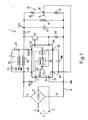
- FIG.1 A known circuit of the aforementioned type to which the preamble of claim 1 refers, is shown by way of reference in Fig.1, wherein the power supply circuit is indicated as a whole by 1 and substantially comprises a rectifying bridge 2 having input terminals 3 between which a sinusoidal input voltage V M is present, and output terminals 5, 6. Terminal 5 is connected, via resistor 5a, to the input pin 7 of a control circuit 8, normally an integrated circuit; and terminal 6 to a reference potential line (ground) 9. Output terminal 5 is also connected to one terminal of winding 10 of transformer 11, the other terminal of which is connected to the anode of diode 12.
- Transformer 11 comprises a second winding 20 having one terminal grounded, and the other terminal connected to pin 21 of control circuit 8, via resistor 20a, and to the anode of diode 22. Between the cathode of diode 22 and ground, there is provided a capacitor 23, and the cathode of diode 22 is also connected to pin 24 of control circuit 8.
- Control circuit 8 substantially comprises an error amplifier 27 having the positive input connected to reference voltage V R , and the negative input connected to input pin 19 of control circuit 8. Between the inverting input and the output of error amplifier 27, there is connected a compensating capacitor 28 normally external to control circuit 8 and connected between input pin 19 and a further input pin 29 of circuit 8.
- the output of error amplifier 27 is connected to one input of a multiplier stage 30, a second input of which is connected to pin 7, and the output of which is connected to a control stage 31 also connected to pin 24.
- the output of control stage 31 is connected to the gate terminal of a power MOS transistor 34.
- Control stage 31 comprises the control logic for turning transistor 34 on and off, and also provides for driving transistor 34, which presents the drain terminal connected to the anode of diode 12, and the source terminal connected to pin 35 of control circuit 8. Finally, a resistor 36 is provided between the source terminal of transistor 34 and ground, and control circuit 8 presents a pin 37 connected to ground line 9.
- Fig.1 circuit fails to instantly eliminate sharp overvoltages at the output caused, for example, by a sharp variation in load 14. This is due to the limited response of control circuit 8, which must be so designed as to be unaffected by variations in output voltage of twice the frequency of input voltage V M .
- a further divider is provided at the output, in parallel to divider 15, for picking up a signal proportional to the instantaneous value of output voltage V o .
- the tap of the additional divider is connected to the input of a hysteresis comparator built into control circuit 8 and which compares the incoming signal with a reference voltage and, in the event this is exceeded, supplies a turn-off signal to control stage 31, which turns off transistor 34 until output voltage V o is restored to the correct value.
- Russian Inventions Illustrated, Derwent Publication Ltd., SU-A-1 350 828 discloses an A/D signal processing amplifier-limiter, including an input operational amplifier connected in inverted mode by a feedback network including a capacitor and base-to-emitter junctions.
- the operational amplifier does not operate in linear mode, and the base-to-emitter junctions belong to two current flow direction sensors, the outputs whereof are connected to comparators and to a coincidence gate to control three switches determining the polarity of the output voltage.
- the output voltage of the circuit is not controlled through the operational amplifier and the current sensors do not generate signals proportional to the variations of the circuit output voltage with respect to a preset value (output voltage error).
- EP-A-0 113 745 discloses a step waveform generator including an input operational amplifier having a feedback network including a current mirror. Also here, the operational amplifier does not operate as an error amplifier, the output voltage of the circuit is not controlled by the operational amplifier, and no current sensor for detecting the current flowing at the output of the operational amplifier and for generating a signal proportional to the variation of the circuit output voltage is present.
- a device comprising an error amplifier, a control portion and a circuit for detecting voltage variations in relation to a set value, as claimed in Claim 1.
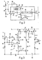
- Fig.2 only control circuit 8, compensating capacitor 28, divider 15 and transistor 34 of pbwer supply circuit 1 are shown, all the other components being identical to those in Fig.1 and having no bearing on the following description. Wherever possible, any parts in common with the Fig.1 diagram are indicated using the same reference numbers.
- Number 40 in Fig.2 indicates a circuit for detecting variations in output voltage in relation to a set value, and which, according to the present invention, comprises means for detecting the current through compensating capacitor 28, which current is instantly proportional to variations in output voltage V o . Said means are advantageously integrated in control circuit 8 for eliminating the need for an additional pin on the package.
- detecting circuit comprises a current sensor 40, here located between pin 29 and output 41 of error amplifier 27, for generating at output 42 a signal KDI proportional to the current in capacitor 28.
- current signal KDI is converted into a voltage signal via a resistor 43 between output 42 of sensor 40 and ground, and is supplied to the negative input of a hysteresis comparator 44, the positive input of which presents reference potential V R1 .
- the output of hysteresis comparator 44 is supplied to control and drive stage 31 for turning off transistor 34 when the output voltage exceeds the threshold defined by reference potential V R1 .
- the Fig.2 circuit operates as follows.
- the current through resistor 17, located between tap 18 and ground and of resistance R 1 may be considered constant and equal to V R /R 1 , by virtue of resistor 17 being connected to the inverting input of error amplifier 27.
- V o of power supply circuit 1 equals the set value
- said current is also equal to the current through resistor 16 connected to the cathode of diode 12 (Fig.1) and of resistance R 2 .
- current DI through capacitor 28 is determined by current sensor 40 as the difference between the instantaneous current through the output stage of error amplifier 27 and the bias current of the same, by virtue of both, as stated, being equal under steady state operating conditions of the power supply circuit.
- amplifier 27 is represented by a preamplifier 47 and a final stage including an output transistor 48 and a current source 49 supplying bias current I b .
- preamplifier 47 presents a positive input at reference potential V R , a negative input connected to pin 19 (and consequently tap 18), and the output 50 connected to the base terminal of output transistor 48, in this case a PNP type.
- the emitter terminal of transistor 48 defines output 41 of error amplifier 27, while the collector terminal is connected to that of an NPN type transistor 51 of a current mirror circuit 52 forming part of current sensor 40.
- Transistor 51 presents its emitter connected to ground line 9 (via pin 37), and its base shortcircuited with the collector and connected to the base of an NPN type transistor 53 forming current mirror circuit 52 together with transistor 51.
- Transistor 53 presents its emitter grounded and its collector connected to that of a transistor 55 forming a current mirror circuit 57 together with transistor 56.
- Transistors 55 and 56 are both PNP types, and present mutually connected bases, and emitters connected to a supply line 58 at potential V CC .
- Transistor 56 presents its base terminal shortcircuited with the collector terminal, and a current source 49 is provided between the collector of transistor 56 and output node 41 of error amplifier 27, for supplying current I b to transistor 48.
- Node 60 between the collector terminals of transistors 55 and 53 is connected to the collector terminal of a further transistor 61 forming, with transistor 62, a 1:K ratio current mirror circuit 63.
- Transistors 61 and 62 are both PNP types, and present mutually connected base terminals, and emitter terminals connected to supply line 58.
- Transistor 61 presents its collector terminal shortcircuited with its base terminal;
- transistor 62 presents its collector terminal connected to one terminal of resistor 43 via node 64; and node 64 is connected to the negative input of hysteresis comparator 44.
- an increase DV o at the power supply circuit output results in an increase DI in the current of resistor 16, which current flows into capacitor 28 and is injected into output transistor 48, which, at this phase, is supplied with current I b + DI.
- Transistor 61 is thus supplied at this phase with current DI, equal to the difference between the current supplied by transistor 55 and that (I b + DI) drawn by transistor 53, and, according to the ratio K between the emitter areas of transistors 61 and 62, mirrors it to transistor 62.
- the resulting current KDI is supplied to resistor 43, which accordingly generates a voltage drop V 1 proportional to variation DV o and which, when it exceeds threshold V R1 , activates hysteresis comparator 44 for turning off MOS transistor 34.
- the overvoltage detecting components may be integrated in control circuit 8 with no need for a special pin. This therefore provides, not only for fully implementing the overvoltage detecting and limiting circuit on control circuits 8 with an insufficient number of pins, but also, in the case of control circuits with several available pins, for freeing an additional pin for other purposes.
- any errors or percentage inaccuracy in reference voltage V R1 and/or in the measurement of current DI result in an activation error of hysteresis comparator 44 as a function of voltage variation DV o , and, as compared with the overall error of output voltage V o , are thus reduced by a factor equal to DV o /V o .
- the circuit described provides for a high degree of reliability, and may be rendered extremely accurate, despite possible production spread in resistance and the sensitivity of resistor 43 to variations in temperature.
- any spread in the resistance of resistor 43 may be overcome by simply calibrating the circuit accordingly, e.g. by adjusting the resistance of resistor 16 as described above, or by calibrating resistor 43; while the sensitivity of resistor 43 to variations in temperature may be overcome quite simply by reference potential V R1 varying as a function of temperature in the same way as the resistance of resistor 43.
- circuits may also be applied to other types of devices having an output at which overvoltage is to be detected and possibly limited, and comprising error amplifiers having a feedback branch which, under steady state operating conditions, is not supplied with current, and, in the event of a variation in the output voltage of the device, is supplied with current instantly proportional to the voltage variation.
- circuit according to the present invention may also be applied to devices involving no restriction in the number of pins, or in which the detecting circuit need not necessarily be integrated.
- the same design solution may also be applied for detecting and possibly limiting negative variations in set voltage, in which case also, current only flows through the feedback capacitor, though inverted as compared with the example described, under other than steady state operating conditions of the device. In this case, appropriate changes may obviously be required to the detecting and limiting circuit.
Priority Applications (4)
| Application Number | Priority Date | Filing Date | Title |
|---|---|---|---|
| EP92830428A EP0580923B1 (en) | 1992-07-30 | 1992-07-30 | Device comprising an error amplifier, a control portion and a circuit for detecting voltage variations in relation to a set value |
| DE69222762T DE69222762T2 (de) | 1992-07-30 | 1992-07-30 | Steuerungsteil und Fehlerverstärker enthaltende Vorrichtung mit einer Schaltung zum Messen der auf einen Spannungssollwert bezogenen Spannungsschwankungen |
| JP17551393A JP3240216B2 (ja) | 1992-07-30 | 1993-07-15 | 設定値に対する電圧変動を検出する検出回路、デバイス及び電力供給回路 |
| US08/100,482 US5589759A (en) | 1992-07-30 | 1993-07-30 | Circuit for detecting voltage variations in relation to a set value, for devices comprising error amplifiers |
Applications Claiming Priority (1)
| Application Number | Priority Date | Filing Date | Title |
|---|---|---|---|
| EP92830428A EP0580923B1 (en) | 1992-07-30 | 1992-07-30 | Device comprising an error amplifier, a control portion and a circuit for detecting voltage variations in relation to a set value |
Publications (2)
| Publication Number | Publication Date |
|---|---|
| EP0580923A1 EP0580923A1 (en) | 1994-02-02 |
| EP0580923B1 true EP0580923B1 (en) | 1997-10-15 |
Family
ID=8212150
Family Applications (1)
| Application Number | Title | Priority Date | Filing Date |
|---|---|---|---|
| EP92830428A Expired - Lifetime EP0580923B1 (en) | 1992-07-30 | 1992-07-30 | Device comprising an error amplifier, a control portion and a circuit for detecting voltage variations in relation to a set value |
Country Status (4)
| Country | Link |
|---|---|
| US (1) | US5589759A (ja) |
| EP (1) | EP0580923B1 (ja) |
| JP (1) | JP3240216B2 (ja) |
| DE (1) | DE69222762T2 (ja) |
Families Citing this family (45)
| Publication number | Priority date | Publication date | Assignee | Title |
|---|---|---|---|---|
| US5745352A (en) * | 1994-10-27 | 1998-04-28 | Sgs-Thomson Microelectronics S.R.L. | DC-to-DC converter functioning in a pulse-skipping mode with low power consumption and PWM inhibit |
| JP3920371B2 (ja) * | 1996-01-29 | 2007-05-30 | 富士通株式会社 | 充電装置、電流検出回路、及び、電圧検出回路 |
| US5764040A (en) * | 1996-09-24 | 1998-06-09 | Intel Corporation | Transient tolerant power supply method and apparatus |
| JP2001161025A (ja) * | 1999-11-30 | 2001-06-12 | Ando Electric Co Ltd | 電流制限装置 |
| JP4640739B2 (ja) * | 2000-11-17 | 2011-03-02 | ローム株式会社 | 安定化直流電源装置 |
| FR2835664B1 (fr) * | 2002-02-04 | 2004-04-16 | St Microelectronics Sa | Procede de generation d'une rampe de tension aux bornes d'un condensateur, et dispositif electronique correspondant, en particulier pour une alimentation a decoupage d'un telephone mobile cellulaire |
| JP4744945B2 (ja) * | 2004-07-27 | 2011-08-10 | ローム株式会社 | レギュレータ回路 |
| US7852017B1 (en) * | 2007-03-12 | 2010-12-14 | Cirrus Logic, Inc. | Ballast for light emitting diode light sources |
| US8018171B1 (en) | 2007-03-12 | 2011-09-13 | Cirrus Logic, Inc. | Multi-function duty cycle modifier |
| US8076920B1 (en) | 2007-03-12 | 2011-12-13 | Cirrus Logic, Inc. | Switching power converter and control system |
| US7667408B2 (en) * | 2007-03-12 | 2010-02-23 | Cirrus Logic, Inc. | Lighting system with lighting dimmer output mapping |
| US8723438B2 (en) * | 2007-03-12 | 2014-05-13 | Cirrus Logic, Inc. | Switch power converter control with spread spectrum based electromagnetic interference reduction |
| US7554473B2 (en) | 2007-05-02 | 2009-06-30 | Cirrus Logic, Inc. | Control system using a nonlinear delta-sigma modulator with nonlinear process modeling |
| US8102127B2 (en) | 2007-06-24 | 2012-01-24 | Cirrus Logic, Inc. | Hybrid gas discharge lamp-LED lighting system |
| US8008898B2 (en) * | 2008-01-30 | 2011-08-30 | Cirrus Logic, Inc. | Switching regulator with boosted auxiliary winding supply |
| US8576589B2 (en) | 2008-01-30 | 2013-11-05 | Cirrus Logic, Inc. | Switch state controller with a sense current generated operating voltage |
| US8022683B2 (en) * | 2008-01-30 | 2011-09-20 | Cirrus Logic, Inc. | Powering a power supply integrated circuit with sense current |
| US8008902B2 (en) | 2008-06-25 | 2011-08-30 | Cirrus Logic, Inc. | Hysteretic buck converter having dynamic thresholds |
| US8111539B2 (en) * | 2008-06-27 | 2012-02-07 | Sandisk 3D Llc | Smart detection circuit for writing to non-volatile storage |
| US8212491B2 (en) * | 2008-07-25 | 2012-07-03 | Cirrus Logic, Inc. | Switching power converter control with triac-based leading edge dimmer compatibility |
| US8344707B2 (en) | 2008-07-25 | 2013-01-01 | Cirrus Logic, Inc. | Current sensing in a switching power converter |
| US8279628B2 (en) | 2008-07-25 | 2012-10-02 | Cirrus Logic, Inc. | Audible noise suppression in a resonant switching power converter |
| US8130528B2 (en) | 2008-08-25 | 2012-03-06 | Sandisk 3D Llc | Memory system with sectional data lines |
| US8487546B2 (en) * | 2008-08-29 | 2013-07-16 | Cirrus Logic, Inc. | LED lighting system with accurate current control |
| US8179110B2 (en) | 2008-09-30 | 2012-05-15 | Cirrus Logic Inc. | Adjustable constant current source with continuous conduction mode (“CCM”) and discontinuous conduction mode (“DCM”) operation |
| US8222872B1 (en) | 2008-09-30 | 2012-07-17 | Cirrus Logic, Inc. | Switching power converter with selectable mode auxiliary power supply |
| US8288954B2 (en) * | 2008-12-07 | 2012-10-16 | Cirrus Logic, Inc. | Primary-side based control of secondary-side current for a transformer |
| US8299722B2 (en) | 2008-12-12 | 2012-10-30 | Cirrus Logic, Inc. | Time division light output sensing and brightness adjustment for different spectra of light emitting diodes |
| US8362707B2 (en) * | 2008-12-12 | 2013-01-29 | Cirrus Logic, Inc. | Light emitting diode based lighting system with time division ambient light feedback response |
| CN101762734B (zh) * | 2008-12-23 | 2012-09-19 | 台达电子工业股份有限公司 | 输出电压检测电路及交换式电源供应器 |
| US7994863B2 (en) * | 2008-12-31 | 2011-08-09 | Cirrus Logic, Inc. | Electronic system having common mode voltage range enhancement |
| US8279650B2 (en) | 2009-04-20 | 2012-10-02 | Sandisk 3D Llc | Memory system with data line switching scheme |
| US8482223B2 (en) * | 2009-04-30 | 2013-07-09 | Cirrus Logic, Inc. | Calibration of lamps |
| US8963535B1 (en) | 2009-06-30 | 2015-02-24 | Cirrus Logic, Inc. | Switch controlled current sensing using a hall effect sensor |
| US8212493B2 (en) * | 2009-06-30 | 2012-07-03 | Cirrus Logic, Inc. | Low energy transfer mode for auxiliary power supply operation in a cascaded switching power converter |
| US8248145B2 (en) * | 2009-06-30 | 2012-08-21 | Cirrus Logic, Inc. | Cascode configured switching using at least one low breakdown voltage internal, integrated circuit switch to control at least one high breakdown voltage external switch |
| US8198874B2 (en) | 2009-06-30 | 2012-06-12 | Cirrus Logic, Inc. | Switching power converter with current sensing transformer auxiliary power supply |
| US9155174B2 (en) * | 2009-09-30 | 2015-10-06 | Cirrus Logic, Inc. | Phase control dimming compatible lighting systems |
| US9178415B1 (en) | 2009-10-15 | 2015-11-03 | Cirrus Logic, Inc. | Inductor over-current protection using a volt-second value representing an input voltage to a switching power converter |
| US8654483B2 (en) | 2009-11-09 | 2014-02-18 | Cirrus Logic, Inc. | Power system having voltage-based monitoring for over current protection |
| US8536799B1 (en) | 2010-07-30 | 2013-09-17 | Cirrus Logic, Inc. | Dimmer detection |
| US8569972B2 (en) | 2010-08-17 | 2013-10-29 | Cirrus Logic, Inc. | Dimmer output emulation |
| CN102723658B (zh) * | 2012-04-23 | 2013-09-25 | 四川马尔斯科技有限责任公司 | 一种激光器的恒流源供电电路 |
| US9134743B2 (en) | 2012-04-30 | 2015-09-15 | Infineon Technologies Austria Ag | Low-dropout voltage regulator |
| JP6085495B2 (ja) * | 2013-02-26 | 2017-02-22 | ルネサスエレクトロニクス株式会社 | 半導体装置 |
Family Cites Families (19)
| Publication number | Priority date | Publication date | Assignee | Title |
|---|---|---|---|---|
| JPS583626B2 (ja) * | 1977-08-12 | 1983-01-22 | 日本ビクター株式会社 | 同期分離回路におけるノイズ消去回路 |
| EP0113745A1 (en) | 1982-07-15 | 1984-07-25 | KENRICK & JEFFERSON LIMITED | Envelopes |
| EP0123745B1 (en) * | 1983-04-29 | 1987-09-02 | International Business Machines Corporation | A step waveform generator and crt vertical timebase incorporating such a generator |
| US4542330A (en) | 1983-10-04 | 1985-09-17 | Hughes Aircraft Company | Low input voltage precision DC-to-DC voltage converter circuit |
| JPH0623937B2 (ja) * | 1984-05-23 | 1994-03-30 | 日新電機株式会社 | 電圧連続可変型直流発生装置 |
| SU1350829A1 (ru) * | 1986-02-18 | 1987-11-07 | Московский Инженерно-Физический Институт | Усилитель-ограничитель |
| US4701720A (en) * | 1986-04-28 | 1987-10-20 | National Semiconductor Corporation | Capacitive feedback to boost amplifier slew rate |
| SU1350828A1 (ru) | 1986-06-24 | 1987-11-07 | Московский энергетический институт | Адаптивный след щий фильтр |
| DE3838408A1 (de) * | 1988-11-12 | 1990-05-17 | Ant Nachrichtentech | Verfahren zum betreiben eines bootsreglers sowie anordnung |
| US4924170A (en) * | 1989-01-03 | 1990-05-08 | Unisys Corporation | Current sharing modular power supply |
| JPH0754336B2 (ja) * | 1989-01-04 | 1995-06-07 | 日産自動車株式会社 | 電流センス回路 |
| US4940929A (en) * | 1989-06-23 | 1990-07-10 | Apollo Computer, Inc. | AC to DC converter with unity power factor |
| US5019952A (en) * | 1989-11-20 | 1991-05-28 | General Electric Company | AC to DC power conversion circuit with low harmonic distortion |
| JPH0415887A (ja) * | 1990-05-09 | 1992-01-21 | Mitsubishi Electric Corp | 演算増幅回路 |
| US5166871A (en) * | 1990-08-31 | 1992-11-24 | International Business Machines Corporation | Buck switching regulator with tow control loops |
| GB9104070D0 (en) * | 1991-02-27 | 1991-04-17 | Astec Int Ltd | Power supplies |
| US5146398A (en) * | 1991-08-20 | 1992-09-08 | Led Corporation N.V. | Power factor correction device provided with a frequency and amplitude modulated boost converter |
| US5177676A (en) * | 1991-09-27 | 1993-01-05 | Exide Electronics Corporation | Voltage source with enhanced source impedance control |
| US5404093A (en) * | 1993-01-05 | 1995-04-04 | Allied Signal Inc. | Low distortion alternating current output active power factor correction circuit using capacitor coupled bi-directional switching regulator |
-
1992
- 1992-07-30 DE DE69222762T patent/DE69222762T2/de not_active Expired - Fee Related
- 1992-07-30 EP EP92830428A patent/EP0580923B1/en not_active Expired - Lifetime
-
1993
- 1993-07-15 JP JP17551393A patent/JP3240216B2/ja not_active Expired - Lifetime
- 1993-07-30 US US08/100,482 patent/US5589759A/en not_active Expired - Lifetime
Non-Patent Citations (1)
| Title |
|---|
| JOURNAL OF PHYSICS E/SCIENTIFIC INSTRUMENTS, June 1987, Bristol, GB, pages 634-635 * |
Also Published As
| Publication number | Publication date |
|---|---|
| JP3240216B2 (ja) | 2001-12-17 |
| JPH06174762A (ja) | 1994-06-24 |
| DE69222762T2 (de) | 1998-02-12 |
| US5589759A (en) | 1996-12-31 |
| DE69222762D1 (de) | 1997-11-20 |
| EP0580923A1 (en) | 1994-02-02 |
Similar Documents
| Publication | Publication Date | Title |
|---|---|---|
| EP0580923B1 (en) | Device comprising an error amplifier, a control portion and a circuit for detecting voltage variations in relation to a set value | |
| US5081379A (en) | Current-sensing circuit for an ic power semiconductor device | |
| US6885177B2 (en) | Switching regulator and slope correcting circuit | |
| JPH03201818A (ja) | 比較回路 | |
| US4801816A (en) | Generator of periodial signals, in particular for switch-mode power supplies | |
| WO1989012348A1 (en) | Voltage drop detector circuit | |
| US5144172A (en) | Detection circuit of the current in an mos type power transistor | |
| US6930539B2 (en) | Reference voltage circuit and method of generating a reference voltage | |
| EP0238803B1 (en) | Stabilized power-supply circuit | |
| US4496885A (en) | Positioning control system | |
| US4541389A (en) | Current regulator for an electromagnetic load utilized in conjunction with an internal combustion engine | |
| US20030137854A1 (en) | Stabilized direct-current power supply device | |
| US7612550B2 (en) | Dropper type regulator | |
| US4319173A (en) | Dual polarity fast discharge integrator apparatus | |
| US4262220A (en) | Optical current isolator circuit | |
| EP0081891B1 (en) | Fixed frequency voltage regulator | |
| US5631549A (en) | Linear regulator power supply with an overcurrent protection device | |
| EP0112380B1 (en) | Frequency to current converter circuit | |
| JPH08223013A (ja) | 電力用トランジスタの過電流保護装置 | |
| JPH04295222A (ja) | 安定化電源回路 | |
| JP3267108B2 (ja) | モータの制御装置 | |
| JPH05291918A (ja) | 混成集積回路 | |
| JPH0612926B2 (ja) | 制御装置の保護回路 | |
| JP2000066747A (ja) | 定電圧回路及びその定電圧出力方法 | |
| JPH0744248A (ja) | 定電圧回路 |
Legal Events
| Date | Code | Title | Description |
|---|---|---|---|
| PUAI | Public reference made under article 153(3) epc to a published international application that has entered the european phase |
Free format text: ORIGINAL CODE: 0009012 |
|
| AK | Designated contracting states |
Kind code of ref document: A1 Designated state(s): DE FR GB IT |
|
| 17P | Request for examination filed |
Effective date: 19931203 |
|
| 17Q | First examination report despatched |
Effective date: 19940308 |
|
| GRAG | Despatch of communication of intention to grant |
Free format text: ORIGINAL CODE: EPIDOS AGRA |
|
| RTI1 | Title (correction) | ||
| GRAH | Despatch of communication of intention to grant a patent |
Free format text: ORIGINAL CODE: EPIDOS IGRA |
|
| GRAH | Despatch of communication of intention to grant a patent |
Free format text: ORIGINAL CODE: EPIDOS IGRA |
|
| GRAA | (expected) grant |
Free format text: ORIGINAL CODE: 0009210 |
|
| AK | Designated contracting states |
Kind code of ref document: B1 Designated state(s): DE FR GB IT |
|
| ITF | It: translation for a ep patent filed |
Owner name: STUDIO TORTA S.R.L. |
|
| REF | Corresponds to: |
Ref document number: 69222762 Country of ref document: DE Date of ref document: 19971120 |
|
| ET | Fr: translation filed | ||
| PLBE | No opposition filed within time limit |
Free format text: ORIGINAL CODE: 0009261 |
|
| STAA | Information on the status of an ep patent application or granted ep patent |
Free format text: STATUS: NO OPPOSITION FILED WITHIN TIME LIMIT |
|
| RAP4 | Party data changed (patent owner data changed or rights of a patent transferred) |
Owner name: STMICROELECTRONICS S.R.L. |
|
| 26N | No opposition filed | ||
| REG | Reference to a national code |
Ref country code: GB Ref legal event code: IF02 |
|
| PGFP | Annual fee paid to national office [announced via postgrant information from national office to epo] |
Ref country code: DE Payment date: 20020807 Year of fee payment: 11 |
|
| PG25 | Lapsed in a contracting state [announced via postgrant information from national office to epo] |
Ref country code: DE Free format text: LAPSE BECAUSE OF NON-PAYMENT OF DUE FEES Effective date: 20040203 |
|
| PGFP | Annual fee paid to national office [announced via postgrant information from national office to epo] |
Ref country code: FR Payment date: 20040708 Year of fee payment: 13 |
|
| PGFP | Annual fee paid to national office [announced via postgrant information from national office to epo] |
Ref country code: GB Payment date: 20040728 Year of fee payment: 13 |
|
| PG25 | Lapsed in a contracting state [announced via postgrant information from national office to epo] |
Ref country code: IT Free format text: LAPSE BECAUSE OF NON-PAYMENT OF DUE FEES;WARNING: LAPSES OF ITALIAN PATENTS WITH EFFECTIVE DATE BEFORE 2007 MAY HAVE OCCURRED AT ANY TIME BEFORE 2007. THE CORRECT EFFECTIVE DATE MAY BE DIFFERENT FROM THE ONE RECORDED. Effective date: 20050730 Ref country code: GB Free format text: LAPSE BECAUSE OF NON-PAYMENT OF DUE FEES Effective date: 20050730 |
|
| GBPC | Gb: european patent ceased through non-payment of renewal fee |
Effective date: 20050730 |
|
| PG25 | Lapsed in a contracting state [announced via postgrant information from national office to epo] |
Ref country code: FR Free format text: LAPSE BECAUSE OF NON-PAYMENT OF DUE FEES Effective date: 20060331 |
|
| REG | Reference to a national code |
Ref country code: FR Ref legal event code: ST Effective date: 20060331 |