EP0575829A2 - Serieller Zugriffspeicher mit Spaltenaddressenzähler und Zeigern - Google Patents
Serieller Zugriffspeicher mit Spaltenaddressenzähler und Zeigern Download PDFInfo
- Publication number
- EP0575829A2 EP0575829A2 EP93109309A EP93109309A EP0575829A2 EP 0575829 A2 EP0575829 A2 EP 0575829A2 EP 93109309 A EP93109309 A EP 93109309A EP 93109309 A EP93109309 A EP 93109309A EP 0575829 A2 EP0575829 A2 EP 0575829A2
- Authority
- EP
- European Patent Office
- Prior art keywords
- signal
- memory
- block
- generate
- column
- Prior art date
- Legal status (The legal status is an assumption and is not a legal conclusion. Google has not performed a legal analysis and makes no representation as to the accuracy of the status listed.)
- Granted
Links
Images


Classifications
-
- G—PHYSICS
- G06—COMPUTING; CALCULATING OR COUNTING
- G06F—ELECTRIC DIGITAL DATA PROCESSING
- G06F5/00—Methods or arrangements for data conversion without changing the order or content of the data handled
- G06F5/06—Methods or arrangements for data conversion without changing the order or content of the data handled for changing the speed of data flow, i.e. speed regularising or timing, e.g. delay lines, FIFO buffers; over- or underrun control therefor
- G06F5/16—Multiplexed systems, i.e. using two or more similar devices which are alternately accessed for enqueue and dequeue operations, e.g. ping-pong buffers
-
- G—PHYSICS
- G11—INFORMATION STORAGE
- G11C—STATIC STORES
- G11C8/00—Arrangements for selecting an address in a digital store
- G11C8/04—Arrangements for selecting an address in a digital store using a sequential addressing device, e.g. shift register, counter
Definitions
- This invention relates to a method of selecting successive columns in successive memory blocks in a serial access memory.
- serial access memory is a first-in-first-out (FIFO) memory that stores serial input data in synchronization with a write clock, and provides the same data in the same order as serial output in synchronization with a read clock.
- FIFO first-in-first-out
- Such memories are often used as line memories or frame memories in image-processing apparatus.
- the memory stores data in a row-and-column array of memory cells. In access to a given row, successive columns in that row are selected by shifting a pulse through a shift register clocked by the read or write clock.
- the shift register is configured as a ring counter, so that it repeatedly selects all columns in ascending order.
- each block having its own shift registers for read and write access.
- the shift register design must now be modified, because each row extends through a plurality of blocks.
- the conventional modification connects the output end of each shift register to the input end of the shift register in the next block, so that a plurality of shift registers form a single ring counter. This leads, however, to two problems.
- Another object is to raise the operating speed of a serial access memory.
- serial access memory data are stored in row-and-column arrays of memory cells in a plurality of memory blocks, and access is synchronized with a clock signal.
- a column address counter counts the clock signal to generate a column address.
- a block selector decodes upper bits of the column address to generate a series of block select signals, which are input to respective memory blocks.
- a shift register receives and shifts one block select signal, thereby generating a series of column select signals that select successive columns in that memory block.
- Fig. 1 is a general block diagram illustrating the invented serial access memory.
- Fig. 2 is a more detailed block diagram illustrating a memory block and its row-selecting circuits.
- Fig. 3 is a more detailed block diagram illustrating column-selecting circuits.
- Fig. 4 is a circuit diagram of the block selector in Fig. 3.
- Fig. 5 is a timing diagram illustrating the operation of the column address counter and block selector.
- Fig. 6 is a circuit diagram illustrating a configuration of the shift register in Fig. 3.
- Fig. 7 illustrates a modification of Fig. 6.
- each of the four memory blocks MB1, MB2, MB3, and MB4 comprises a memory cell array 2 and two shift registers 4 and 6.
- the shift register 4 will be referred to as the read pointer; the shift register 6 will be referred to as the write pointer.
- Each memory cell array 2 has memory cells arranged in, for example, two hundred fifty-six rows and two hundred fifty-six columns. The read and write pointers 4 and 6 select the columns.
- the memory also comprises a read column address counter 8, a write column address counter 10, a read block selector 12, and a write block selector 14.
- the read and write column address counters 8 and 10 are ten-bit counters.
- the read column address counter 8 is incremented by a read clock signal RCK;
- the write column address counter 10 is incremented by a write clock signal WCK.
- the read block selector 12 receives the two upper bits of the read column address count generated by the read column address counter 8 and decodes these two upper bits to generate four read block select pulses RBS1, RBS2, RBS3, and RBS4, which are supplied to the read pointers 4 in memory blocks MB1, MB2, MB3, and MB4, respectively.
- the write block selector 14 similarly decodes the two upper bits of the write column address count to generate four write block select pulses WBS1, WBS2, WBS3, and WBS4, which are supplied to the write pointers 6 in memory blocks MB1, MB2, MB3, and MB4, respectively.
- Fig. 2 shows in more detail the circuits associated with a memory cell array 2 for selecting rows and transferring data.
- the rows correspond to word lines WL, which cross the memory cell array 2 in the vertical direction in the drawing.
- Columns correspond to bit lines BL, which cross the memory cell array 2 in the horizontal direction in the drawing.
- Memory cells are disposed at the intersections of the word lines and bit lines, each memory cell being coupled to one word line and one bit line.
- Rows are selected by a read row address counter 16, a write row address counter 18, an address multiplexer 20, and a row decoder 22.
- the read and write row address counters 16 and 18 are up-counters that generate, for example, eight-bit row addresses.
- the address multiplexer 20 selects the row address output from either the read row address counter 16 or the write row address counter 18 for provision to the row decoder 22.
- the row decoder 22 decodes the provided address and drives one of the word lines WL to the active state.
- Bits of read data are transferred out of the memory cell array 2 to a read data bus DBR by a transfer circuit 24, a line buffer 26, an input/output (I/O) circuit 28, a driver circuit 30, and the read pointer 4.
- the transfer circuit 24 comprises switches, such as transistor switches, that all turn on or off simultaneously.
- the bit lines are coupled through these switches to the line buffer 26, which is a parallel register for storing two hundred fifty-six bits of data.
- the line buffer 26 is coupled through switches in the I/O circuit 28 to the read data bus DBR.
- the read pointer 4 selects one column at a time, causing the driver circuit 30 to turn on one switch at a time in the I/O circuit 28, thereby transferring one bit at a time from the line buffer 26 to the read data bus DBR.
- Bits of write data are transferred from a write data bus DBW into the memory cell array 2 by the write pointer 6 and a driver circuit 32, an I/O circuit 34, a line buffer 36, and a transfer circuit 38.
- the write pointer 6 selects one column at a time, causing the driver circuit 32 to turn on one switch at a time in the I/O circuit 34, thereby transferring one bit at a time from the write data bus DBW into the line buffer 36. From the line buffer 36, the data bits are transferred all at once via the transfer circuit 38 into the memory cell array 2.
- Fig. 3 is a more detailed block diagram of the read pointer 4, read column address counter 8, and read block selector 12, which select columns for read access. Details of the write pointer 6, write column address counter 10, and write block selector 14 are similar, so a separate drawing will be omitted.
- the read clock is a complementary clock comprising two mutually inverse clock signals RCK and RCK ⁇ .
- the read pointer 4 is a shift register comprising two hundred fifty-six stages S0 to S256, which are clocked by the read clock signals RCK and RCK ⁇ so as to shift data from S0 toward S255.
- Column select signals CS0 ⁇ to CS255 ⁇ are output from the corresponding stages. The column select signals are active low.
- the read column address counter 8 comprises, for example, flip-flops R0 to R9 cascaded so as to count cycles of the read clock signal RCK.
- the count held in the read column address counter 8 is a ten-bit column address.
- the flip-flops are synchronized by RCK and RCK ⁇ so that transitions in the count occur at, for example, the fall of RCK.
- the flip-flops R8 and R9 output two pairs of complementary signals denoted RY8, RY8 ⁇ , RY9, and RY9 ⁇ , representing the upper two bits of the column address.
- the read block selector 12 comprises four unit decoders D1, D2, D3, and D4, which decode RY8, RY8 ⁇ , RY9, and RY9 ⁇ to generate the block select pulses RBS1, RBS2, RBS3, and RBS4.
- Fig. 4 shows the circuit configuration of the unit decoder D1.
- a two-input NAND gate 40 performs a NOT-AND logical operation on RY8 ⁇ and RY9 ⁇ and an inverter 42 inverts the result to generate a first signal A.
- a delay line 44 comprising three inverters 46, 48, and 50 coupled in series and capacitors 52 and 54 that capacitively couple the outputs of the inverters 46 and 48 to ground, inverts A to generate a second signal B.
- a two-input NAND gate 56 performs NOT-AND logic on A and B to generate a third signal C.
- a flip-flop 58 clocked by RCK comprising cross-coupled NAND gates 60 and 62, outputs the inverse of C as the first block select signal RBS1. More precisely, the flip-flop 58 outputs the inverse of C when either C or RCK is low, and holds its existing output state when C and RCK are both high.
- the other unit decoders D2, D3, and D4 have the same circuit configuration but different pairs of input signals, as indicated in the drawing.
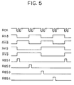
- Fig. 5 illustrates the operation of the read column address counter 8 and read block selector 12.
- RY8 and RY9 are both high and RY8 ⁇ and RY9 ⁇ are both low, indicating that the upper two bits of the column address are both one's.
- the first signal A is low
- the second signal B is high
- the third signal C is high
- RBS1 is low.
- the read column address counter 8 increments from a count of all one's to a count of all zero's, causing RY8 and RY9 to go low and RY8 ⁇ and RY9 ⁇ to go high, the increment occurring at the fall of the read clock RCK.
- the first signal A goes high.
- Both inputs to the NAND gate 56 are now high, so C goes low and RBS1 goes high.
- the read row address counter 16 is adapted to increment at intervals of one thousand twenty-four RCK cycles, and the write row address counter 18 to increment at intervals of one thousand twenty-four WCK cycles.
- the address multiplexer 20 selects the newly incremented read row address
- the row decoder 22 decodes this row address to select a word line WL, and the switches in the transfer circuit 24 are turned on to transfer data from the memory cells connected to that word line into the line buffer 26.
- the address multiplexer 20 selects the newly incremented write row address
- the row decoder 22 decodes this row address to select a word line WL, and the switches in the transfer circuit 38 are turned on to transfer data from the line buffer 36 to memory cells connected to this word line in the memory cell array 2.
- the read and write row address counters 16 and 18 are coordinated with the read and write column address counters so that data are never transferred into and out of the line buffer 26 or the line buffer 36 at the same time.
- the read row address counters in memory blocks MB3 and MB4 can be incremented by the fall of RY9, and the read row address counters in memory blocks MB1 and MB2 by the fall of RY9 ⁇ .
- a first read block select pulse RBS1 When a first read block select pulse RBS1 is generated at the fall of RY9 in Fig. 5, this pulse is input to the read pointer 4 in memory block MB1 as indicated in Fig. 1. Referring to Fig. 3, this pulse is shifted through the two hundred fifty-six stages S0 to S255 of the read pointer 4, causing the column select signals CS0 ⁇ to CS255 ⁇ to go low in turn for one read clock cycle each. Referring to Fig. 2, these column select signals CS0 ⁇ to CS255 ⁇ are fed through the driver circuit 30 to the I/O circuit 28, causing the data stored in the line buffer 26 to be output on the data bus DBR one bit at a time, in ascending column order, during two hundred fifty-six RCK cycles.
- a second read block select pulse RBS2 is output as indicated in Fig. 5 and the same process is repeated in memory block MB2, resulting in the output of two hundred fifty-six bits of data from that memory block.
- a third read block select pulse RBS3 is output and the process is repeated in memory block MB3.
- a fourth read block select pulse RBS4 is output and the same process is repeated to output two hundred fifty-six bits of data from memory block MB4, after which another first read block select pulse RBS1 is output and the whole cycle repeats again with data from a different row.
- the read block selector 12 and write block selector 14 in Fig. 1 can be coupled to the read and write pointers 4 and 6 in the memory blocks by a simple, orderly wiring system, thereby simplifying the design of the memory as compared with the prior art. There are no interconnecting lines between different pointers, so the cycle speed limitations imposed by the parasitic resistance and capacitance of such interconnecting lines are eliminated. These advantages of the invention become increasingly important as the number of memory blocks increases.
- the first stage S0 of this read pointer comprises a first clocked inverter 64, a first latch 66, a second clocked inverter 68, and a second latch 70.
- the first clocked inverter 64 comprises a pair of p-channel metal-oxide-semiconductor field-effect transistors (hereinafter, PMOS transistors) 72 and 74 and a pair of n-channel metal-oxide-semiconductor field-effect transistors (NMOS transistors) 76 and 78 coupled in series between a power supply potential Vcc and a ground potential Vss.
- the PMOS transistor 72 and NMOS transistor 78 are switched on and off by the block select signal RBS1.
- the PMOS transistor 74 is switched by RCK ⁇
- the NMOS transistor 76 by RCK.
- the output node N1 of the first inverter 64 is disposed between the two transistors 74 and 76.
- the first latch 66 comprises a pair of inverters 80 and 82 coupled in a loop, the output of the inverter 80 being coupled to the input of the inverter 82, and the input of the inverter 80 and output of the inverter 82 both being coupled to the signal line of the column select signal CS0 ⁇ .
- This column select signal line is also coupled to the output node N1 of the first inverter 64, and is coupled through a PMOS reset transistor 84 to Vcc.
- the reset transistor 84 is switched by a reset signal RS ⁇ .
- the second inverter 68 is similar to the first, comprising PMOS transistors 86 and 88 and NMOS transistors 90 and 92 coupled in series between Vcc and Vss. However, the PMOS transistor 86 and NMOS transistor 92 are switched by the CS0 ⁇ signal output by the first inverter 64, the PMOS transistor 88 is switched by RCK, and the NMOS transistor 90 is switched by RCK ⁇ .
- the output node N2 of this inverter produces an internal signal K.
- the second latch 70 is similar to the first, comprising a looped pair of inverters 94 and 96 coupled to the output node N2 of the second inverter.
- the next stage S1 is identical to the initial stage S0 except that instead of receiving the block select signal RBS1, it receives the internal signal K. Succeeding stages are the same, each stage receiving the internal signal output by the preceding stage.
- This circuit is initialized by supplying a low reset pulse RS ⁇ to all stages, causing the column select signals CS0 ⁇ to CS255 ⁇ all to go to the high (inactive) state, where they remain as long as RBS1 remains low.
- RBS1 goes high for one read clock cycle, the circuit operates as follows.
- the first inverter 64 In the first half of this clock cycle, when RCK is low and RCK ⁇ is high, the first inverter 64 is disabled (transistors 74 and 76 are switched off), but the first latch 66 continues to hold CS0 ⁇ at the high level.
- the second inverter 68 is enabled (transistors 88 and 90 are switched on) so K is low.
- the first inverter 64 In the second half of this clock cycle, when RCK is high and RCK ⁇ is low, the first inverter 64 is enabled and the second inverter 68 is disabled.
- the first inverter 64 inverts RBS1, driving CS0 ⁇ low, while the second latch 70 holds K low.
- RBS1 goes low but the first latch 66 continues to hold CS0 ⁇ low, while the second inverter 68 inverts CS0 ⁇ and drives K high.
- the first inverter 64 returns CS0 ⁇ to the high level, the second latch 70 continues to hold K high, and the first inverter in the next stage S1 inverts K to drive CS1 ⁇ low.
- Fig. 7 shows a modification of Fig. 6 in which RBS1 is supplied as a set signal to the initial stage S0 and as a reset signal to the other stages S1 to S255.
- Stages S1 to S255 are identical to stage S0 in Fig. 6.
- RBS1 is inverted by an inverter 98 and the inverted signal RBS1 ⁇ is supplied to the reset transistor 84 in each of these stages S1 to S255.
- the reset transistor 84 of Fig. 6 is replaced by an NMOS transistor 99, which is switched by RBS1 and couples node N1 to Vss.
- the input side of stage S0 is also coupled to Vss, and the roles of RCK and RCK ⁇ are reversed.
- the invention can of course be practiced with other shift-register circuits, such as circuits employing flip-flops.
- the invention is not restricted to FIFO serial access memories that generate separate read and write column addresses. It is also applicable to dual-port memories having only a single serial port, which require only a single column address counter, and to various other types of multi-port memories.
- serial access memories already incorporate a column address counter for the purpose of redundant repair, e.g. for selecting redundant bit lines to replace faulty bit lines.
- the invention can be practiced simply by adding a block selector to generate block select signals, thereby obtaining the advantages of simpler signal-line routing and higher-speed operation with minimal increase in chip size.
Landscapes
- Engineering & Computer Science (AREA)
- Theoretical Computer Science (AREA)
- Microelectronics & Electronic Packaging (AREA)
- Physics & Mathematics (AREA)
- General Engineering & Computer Science (AREA)
- General Physics & Mathematics (AREA)
- Dram (AREA)
Applications Claiming Priority (3)
| Application Number | Priority Date | Filing Date | Title |
|---|---|---|---|
| JP16441492A JP3231842B2 (ja) | 1992-06-23 | 1992-06-23 | シリアルアクセスメモリ |
| JP164414/92 | 1992-06-23 | ||
| US08/080,482 US5398209A (en) | 1992-06-23 | 1993-06-18 | Serial access memory with column address counter and pointers |
Publications (3)
| Publication Number | Publication Date |
|---|---|
| EP0575829A2 true EP0575829A2 (de) | 1993-12-29 |
| EP0575829A3 EP0575829A3 (de) | 1995-01-04 |
| EP0575829B1 EP0575829B1 (de) | 1998-09-02 |
Family
ID=26489521
Family Applications (1)
| Application Number | Title | Priority Date | Filing Date |
|---|---|---|---|
| EP93109309A Expired - Lifetime EP0575829B1 (de) | 1992-06-23 | 1993-06-09 | Serieller Zugriffspeicher mit Spaltenaddressenzähler und Zeigern |
Country Status (3)
| Country | Link |
|---|---|
| US (1) | US5398209A (de) |
| EP (1) | EP0575829B1 (de) |
| JP (1) | JP3231842B2 (de) |
Cited By (2)
| Publication number | Priority date | Publication date | Assignee | Title |
|---|---|---|---|---|
| EP0690450A2 (de) * | 1994-06-28 | 1996-01-03 | Nec Corporation | Serielle Zugriffspeicherschaltung durch eine beliebige Addresse |
| EP0788112A2 (de) * | 1996-02-05 | 1997-08-06 | International Business Machines Corporation | Speicher-Adressierschaltung |
Families Citing this family (12)
| Publication number | Priority date | Publication date | Assignee | Title |
|---|---|---|---|---|
| JPH07311842A (ja) * | 1994-05-19 | 1995-11-28 | Konica Corp | 画像記憶装置 |
| JP3380050B2 (ja) * | 1994-07-14 | 2003-02-24 | 富士通株式会社 | 半導体記憶装置のデータ読み出し方法 |
| JP3789173B2 (ja) * | 1996-07-22 | 2006-06-21 | Necエレクトロニクス株式会社 | 半導体記憶装置及び半導体記憶装置のアクセス方法 |
| JPH10334665A (ja) * | 1997-05-30 | 1998-12-18 | Oki Micro Design Miyazaki:Kk | 半導体記憶装置 |
| JPH11305990A (ja) * | 1998-04-24 | 1999-11-05 | Oki Micro Design:Kk | Fifo回路 |
| US6067267A (en) * | 1998-08-12 | 2000-05-23 | Toshiba America Electronic Components, Inc. | Four-way interleaved FIFO architecture with look ahead conditional decoder for PCI applications |
| US6535519B1 (en) | 1998-08-28 | 2003-03-18 | Lsi Logic Corporation | Method and apparatus for data sharing between two different blocks in an integrated circuit |
| JP3574041B2 (ja) * | 2000-04-27 | 2004-10-06 | 株式会社 沖マイクロデザイン | 半導体記憶装置 |
| US6518787B1 (en) * | 2000-09-21 | 2003-02-11 | Triscend Corporation | Input/output architecture for efficient configuration of programmable input/output cells |
| US6532185B2 (en) * | 2001-02-23 | 2003-03-11 | International Business Machines Corporation | Distribution of bank accesses in a multiple bank DRAM used as a data buffer |
| US6956775B1 (en) | 2003-12-31 | 2005-10-18 | Intel Corporation | Write pointer error recovery |
| US11322195B2 (en) * | 2019-11-27 | 2022-05-03 | Taiwan Semiconductor Manufacturing Company, Ltd. | Compute in memory system |
Family Cites Families (2)
| Publication number | Priority date | Publication date | Assignee | Title |
|---|---|---|---|---|
| JP2639650B2 (ja) * | 1987-01-14 | 1997-08-13 | 日本テキサス・インスツルメンツ株式会社 | 半導体装置 |
| JP2582587B2 (ja) * | 1987-09-18 | 1997-02-19 | 日本テキサス・インスツルメンツ株式会社 | 半導体記憶装置 |
-
1992
- 1992-06-23 JP JP16441492A patent/JP3231842B2/ja not_active Expired - Fee Related
-
1993
- 1993-06-09 EP EP93109309A patent/EP0575829B1/de not_active Expired - Lifetime
- 1993-06-18 US US08/080,482 patent/US5398209A/en not_active Expired - Fee Related
Non-Patent Citations (2)
| Title |
|---|
| 1990 SYMPOSIUM ON VLSI CIRCUITS, June 1990, HONOLULU USA pages 51 - 52 KURIYAMA ET AL. 'A 4 MBIT CMOS SRAM WITH 8 NS SERAIL ACCESS TIME' * |
| IEEE JOURNAL OF SOLID-STATE CIRCUITS., vol.26, no.4, April 1991, NEW YORK US pages 502 - 506 KURIYAMA ET AL. 'AN 8 NS 4 MB SERIAL ACCESS MEMORY' * |
Cited By (5)
| Publication number | Priority date | Publication date | Assignee | Title |
|---|---|---|---|---|
| EP0690450A2 (de) * | 1994-06-28 | 1996-01-03 | Nec Corporation | Serielle Zugriffspeicherschaltung durch eine beliebige Addresse |
| EP0690450A3 (de) * | 1994-06-28 | 1996-02-07 | Nec Corporation | Serielle Zugriffspeicherschaltung durch eine beliebige Addresse |
| US5815460A (en) * | 1994-06-28 | 1998-09-29 | Nec Corporation | Memory circuit sequentially accessible by arbitrary address |
| EP0788112A2 (de) * | 1996-02-05 | 1997-08-06 | International Business Machines Corporation | Speicher-Adressierschaltung |
| EP0788112A3 (de) * | 1996-02-05 | 1999-01-27 | International Business Machines Corporation | Speicher-Adressierschaltung |
Also Published As
| Publication number | Publication date |
|---|---|
| EP0575829A3 (de) | 1995-01-04 |
| US5398209A (en) | 1995-03-14 |
| JPH065070A (ja) | 1994-01-14 |
| JP3231842B2 (ja) | 2001-11-26 |
| EP0575829B1 (de) | 1998-09-02 |
Similar Documents
| Publication | Publication Date | Title |
|---|---|---|
| US6011751A (en) | Sychronous semiconductor memory device with burst address counter operating under linear/interleave mode of single data rate/double data rate scheme | |
| US6078546A (en) | Synchronous semiconductor memory device with double data rate scheme | |
| US7630230B2 (en) | Static random access memory architecture | |
| US6411128B2 (en) | Logical circuit for serializing and outputting a plurality of signal bits simultaneously read from a memory cell array or the like | |
| US5398209A (en) | Serial access memory with column address counter and pointers | |
| US5699530A (en) | Circular RAM-based first-in/first-out buffer employing interleaved storage locations and cross pointers | |
| US5212663A (en) | Method to implement a large resettable static RAM without the large surge current | |
| KR100384775B1 (ko) | 쿼드 데이터 레이트 싱크로노스 에스램의 리드/라이트를위한 워드라인 및 비트라인 구동 방법 및 그 회로 | |
| US5513139A (en) | Random access memory with circuitry for concurrently and sequentially writing-in and reading-out data at different rates | |
| US6259648B1 (en) | Methods and apparatus for implementing pseudo dual port memory | |
| EP0363031B1 (de) | Halbleiterspeicher mit Serieneingang/Serienausgang | |
| US7447812B1 (en) | Multi-queue FIFO memory devices that support flow-through of write and read counter updates using multi-port flag counter register files | |
| US4903242A (en) | Serial access memory circuit with improved serial addressing circuit composed of a shift register | |
| US6320794B1 (en) | Late-write type semiconductor memory device with multi-channel data output multiplexer | |
| US6463000B2 (en) | First-in first-out memory device and method of generating flag signal in the same | |
| US5594700A (en) | Sequential memory | |
| JPH0738170B2 (ja) | ランダム・アクセス・メモリ装置 | |
| US4943947A (en) | Semiconductor memory device with an improved serial addressing structure | |
| US6219283B1 (en) | Memory device with local write data latches | |
| US5661693A (en) | Memory device for synchronously reading and writing data | |
| US5255242A (en) | Sequential memory | |
| KR100228455B1 (ko) | 반도체 메모리 회로 | |
| EP0743649A2 (de) | Serieller Zugriffspeicher mit reduzierter Kreisverzögerung | |
| US6590814B1 (en) | Semiconductor memory device and redundancy method thereof | |
| US6629185B1 (en) | Architecture, circuitry and method of transferring data into and/or out of an interdigitated memory array |
Legal Events
| Date | Code | Title | Description |
|---|---|---|---|
| PUAI | Public reference made under article 153(3) epc to a published international application that has entered the european phase |
Free format text: ORIGINAL CODE: 0009012 |
|
| AK | Designated contracting states |
Kind code of ref document: A2 Designated state(s): DE FR NL |
|
| PUAL | Search report despatched |
Free format text: ORIGINAL CODE: 0009013 |
|
| AK | Designated contracting states |
Kind code of ref document: A3 Designated state(s): DE FR NL |
|
| 17P | Request for examination filed |
Effective date: 19950303 |
|
| 17Q | First examination report despatched |
Effective date: 19970620 |
|
| GRAG | Despatch of communication of intention to grant |
Free format text: ORIGINAL CODE: EPIDOS AGRA |
|
| GRAG | Despatch of communication of intention to grant |
Free format text: ORIGINAL CODE: EPIDOS AGRA |
|
| GRAH | Despatch of communication of intention to grant a patent |
Free format text: ORIGINAL CODE: EPIDOS IGRA |
|
| GRAH | Despatch of communication of intention to grant a patent |
Free format text: ORIGINAL CODE: EPIDOS IGRA |
|
| GRAH | Despatch of communication of intention to grant a patent |
Free format text: ORIGINAL CODE: EPIDOS IGRA |
|
| GRAH | Despatch of communication of intention to grant a patent |
Free format text: ORIGINAL CODE: EPIDOS IGRA |
|
| GRAA | (expected) grant |
Free format text: ORIGINAL CODE: 0009210 |
|
| AK | Designated contracting states |
Kind code of ref document: B1 Designated state(s): DE FR NL |
|
| REF | Corresponds to: |
Ref document number: 69320704 Country of ref document: DE Date of ref document: 19981008 |
|
| ET | Fr: translation filed | ||
| PLBE | No opposition filed within time limit |
Free format text: ORIGINAL CODE: 0009261 |
|
| STAA | Information on the status of an ep patent application or granted ep patent |
Free format text: STATUS: NO OPPOSITION FILED WITHIN TIME LIMIT |
|
| 26N | No opposition filed | ||
| PGFP | Annual fee paid to national office [announced via postgrant information from national office to epo] |
Ref country code: FR Payment date: 20020610 Year of fee payment: 10 |
|
| PGFP | Annual fee paid to national office [announced via postgrant information from national office to epo] |
Ref country code: DE Payment date: 20020612 Year of fee payment: 10 |
|
| PGFP | Annual fee paid to national office [announced via postgrant information from national office to epo] |
Ref country code: NL Payment date: 20020628 Year of fee payment: 10 |
|
| PG25 | Lapsed in a contracting state [announced via postgrant information from national office to epo] |
Ref country code: NL Free format text: LAPSE BECAUSE OF NON-PAYMENT OF DUE FEES Effective date: 20040101 Ref country code: DE Free format text: LAPSE BECAUSE OF NON-PAYMENT OF DUE FEES Effective date: 20040101 |
|
| PG25 | Lapsed in a contracting state [announced via postgrant information from national office to epo] |
Ref country code: FR Free format text: LAPSE BECAUSE OF NON-PAYMENT OF DUE FEES Effective date: 20040227 |
|
| NLV4 | Nl: lapsed or anulled due to non-payment of the annual fee |
Effective date: 20040101 |
|
| REG | Reference to a national code |
Ref country code: FR Ref legal event code: ST |