EP0572060A1 - Apparatus and method for resistive detection and waveform analysis of interconnection networks - Google Patents
Apparatus and method for resistive detection and waveform analysis of interconnection networks Download PDFInfo
- Publication number
- EP0572060A1 EP0572060A1 EP93201310A EP93201310A EP0572060A1 EP 0572060 A1 EP0572060 A1 EP 0572060A1 EP 93201310 A EP93201310 A EP 93201310A EP 93201310 A EP93201310 A EP 93201310A EP 0572060 A1 EP0572060 A1 EP 0572060A1
- Authority
- EP
- European Patent Office
- Prior art keywords
- network
- net
- pulse
- tested
- reference plane
- Prior art date
- Legal status (The legal status is an assumption and is not a legal conclusion. Google has not performed a legal analysis and makes no representation as to the accuracy of the status listed.)
- Withdrawn
Links
Images


Classifications
-
- G—PHYSICS
- G01—MEASURING; TESTING
- G01R—MEASURING ELECTRIC VARIABLES; MEASURING MAGNETIC VARIABLES
- G01R31/00—Arrangements for testing electric properties; Arrangements for locating electric faults; Arrangements for electrical testing characterised by what is being tested not provided for elsewhere
- G01R31/28—Testing of electronic circuits, e.g. by signal tracer
- G01R31/2801—Testing of printed circuits, backplanes, motherboards, hybrid circuits or carriers for multichip packages [MCP]
- G01R31/2805—Bare printed circuit boards
Definitions
- the present invention relates to high density circuit boards and ceramic substrates, and more particularly to an apparatus and method for detecting the continuity of an interconnection network and whether such network is shorted to or has a leakage resistance to another interconnection network.
- Circuit boards and ceramic substrates usually include metal interconnection networks (nets), power planes, dielectric materials, and at least one reference plane.
- nets metal interconnection networks
- Each of such circuit boards can in fact comprise multi-layers each having fabricated thereon different nets. Each net may also be distributed across the multi-layers within a circuit board.
- each circuit board i.e. the integrity of the different metal interconnections that effect each of the nets in the circuit board
- defects such as an "open circuit” condition whereby higher than expected resistance appears between certain sections of a network, or a “short circuit” condition whereby two separate nets, which theoretically should have infinite resistance therebetween, in fact appear to be shorted together, or have an unacceptable internet (leakage) resistance, are to be detected and avoided.
- full cluster probes gang probes or bed-of-nails probes
- a number of moving probes serial testing.
- the full cluster probe method detects opens by measuring the resistance between the terminals of the nets, and shorts by measuring the resistance between the being tested net and the rest of the nets.
- the serial testing method detects opens by measuring the resistance of the net, and shorts by measuring the capacitance between the net and a reference plane. Measured excess capacitance indicates that a short exists.
- the serial testing method uses DC resistance meters for open detection and impedance meters such as HP 4284A LCR meter for capacitance measurements.
- Burr performs a series of one point measurements of the capacitance of a network relative to a reference plane. To test the continuity of each net, a resistance measurement is effected between two probes each placed at an end point of the net. To measure excessive internal capacitance between nets, Burr uses conventional sinusoidal AC signal generating devices. See column 5, lines 65-69 of Burr.
- the throughput for short detection based on an AC capacitance measurement method is slow. This is due to the fact that the use of an AC method to detect shorts via capacitance measurement requires that ⁇ R i C n (a quantative relationship) be less than or equal to unity. ( ⁇ is the angular frequency, R i the leakage resistance between the nets, and C n the capacitance of the net to which the being tested net is shorted.) For high leakage resistance, the unity criterion requires that low frequencies be used. So, too, the AC phase sensitive detection method requires that the time constant be set to at least one period of the AC signal. And since the rise time of the AC signal, or more precisely the response thereto, is an exponential function, an input signal having a long duration is required in order to produce a substantially accurate final value.
- the prior art method would interpret a net of 1pF (net to reference plane) and 5 megohms leakage resistance to be a short because its R i C n value is the same as the threshold value set for the definition of short R i and the maximum capacitance C n .
- the present invention system uses a combination resistive detection and waveform sampling.
- two probes placed at corresponding end portions of the net, are used to measure the resistance therebetween.
- the present invention further includes the addition of an external capacitor and an external resistor (connected in parallel to the external capacitor) to the reference plane of the circuit board and the application of a rectangular pulse, from a pulse generator, to one of the probes to stimulate (stress) the net.
- the response from the net is then sampled across the external capacitor as a series of voltage values over time by a transient digital analyzer.
- the leading edge of the signal across the external capacitor which can be extrapolated from the series of voltage values, is reflective of the integrity of the net (i.e. a good net, an open, a short, or has leakage resistance between nets) and thereby the integrity of the circuit board.
- the prior art system and method of detecting shorts of a being tested net 2 to any other net of a circuit board is shown.
- the circuit board has a reference plane, or a power plane, 6.
- reference plane 6 can be external or internal, as in a substrate that has multiple layers each of which may contain multiple nets.
- Each of the nets, as for example net 2 has a certain area which depends on the width and the length thereof. Accordingly, between net 2 and reference plane 6 there is a corresponding capacitance C1. Between net 2 and net 4 there is a resistance R12. Further, there is a capacitance C2 between net 4 and reference plane 6.
- the prior art method locates a capacitance meter 8, one end of which connected to reference plane 6 while the other end to a probe 10, at one of the end points of net 2.
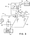
- UUT 14 which comprises nets 16, 18 and reference plane 20 is subjected to resistance detection and waveform sampling.
- UUT 14 may in actuality be comprised of a single circuit board with an external reference plane such as 20, or a substrate having a multiple number of layers of which reference plane 20 may be an internal power or ground plane or external reference plane.
- reference plane 20 may be an internal power or ground plane or external reference plane.
- a plurality of nets, of which only 16 and 18 are shown, may be fabricated on each of the layers.
- the being tested net 16 has positioned at respective end portions thereof a first probe 22 and a second probe 24. Probes 22 and 24 together perform the resistive continuity test to determine whether there is any break at net 16.
- the circuit to which probes 22 and 24 are part of may be referred to as a floating current testing circuit 38.
- the floating current testing circuit 38 also includes a floating current source 26.
- the floating current source can be a floating voltage source 28 and a resistance R s .
- An output of probe 22 is connected via line 30 to one of the inputs of a differential amplifier 32, and the output of probe 24 is connected via line 34 as the other input to differential amplifier 32.
- Floating current source 26 is connected across lines 30 and 34.
- the output of differential amplifier 32 is detected by an analyzer 36 which, for the embodiment of the present invention, may be an Analytek transient digital analyzer having model number 2000P.
- Floating current testing circuit 38 detects the resistance between any two points, as for example the distance separated by probes 22 and 24, along net 16. Such resistance is designated R m . In essence, if there is proper conductivity between any two points, as designated by probes 22 and 24 for example, along net 16, the resistance, if any, between those points is very low. Conversely, if there is improper conductivity, i.e. discontinuity, between any two points along net 16, for example as a result of physical breakage, the resistance between those points are extremely high, as for example, almost infinite. Thus, by determining the resistance between the various points, and particularly the end points, along net 16, its conductivity can be ascertained.
- probes 22 and 24 are each brought into contact with net 16 at respective different locations, for example its respective end points.
- a small current is then provided by floating current source 26 to one of the probes, as for example probe 24.
- the current in net 16 induces voltage potentials at probes 22 and 24 which are sampled by differential amplifier 32. If the resistance of net 16 is low, differential amplifier 32 would detect substantially no potential difference between the different locations. However, if the resistance of net 16 is high, differential amplifier 32 would detect a potential difference between probes 22 and 24, which in turn is detected by analyzer 36. Thus, by detecting the potential difference provided from differential amplifier 32, the conductivity of net 16 is ascertained.
- short testing circuit 40 comprises a probe, for example probe 22, an internal resistance R12 across nets 16 and 18, an internal capacitance C12 across net 16 and 18, a capacitance C1 across net 16 and reference plane 20, and a capacitance C2 between net 18 and reference plane 20.
- short testing circuit 40 There is further included in short testing circuit 40 an external capacitor C0 one end of which is connected to reference plane 20 and the other end of which is connected to a pulse generator 42, which may be grounded.
- Pulse generator 42 has an output provided via line 44 to probe 22. There are a number of pulse generators which may be used for the embodiment of the present invention shown in Fig.
- pulse generator 42 As its name implies, generates pulse signals whose width can be varied.
- analyzer 46 Connected across C0 is an analyzer 46 which may also be an Analytek 2000P transient digital analyzer.
- short detecting circuit 40 operates as follows.
- a rectangular pulse, designated 50 is generated from pulse generator 42 and fed via line 44 to probe 22, which could be placed anywhere along net 16.
- the width and amplitude of the pulse is dependent on the combined characteristics of the different electronic components in the circuit and particularly are dependent on the type of sensitivity required for the circuit and the signal/noise level that is desired. In other words, the higher the required sensitivity for large leakage resistance, the wider the width. So, too, the larger of a signal/noise level desired, the larger the amplitude of the pulse signal.
- the pulse signal is applied by probe 22 to net 16.
- signals having different amplitudes are produced across external capacitor C0.
- An exemplar response signal is shown, for example, in Fig. 7B. The interpretation of the response signal is described later with respect to the different equivalent circuits of Figs. 5-13.
- a quick determination can be made on whether a net is acceptable, i.e. a good net, an opened net, shorted to one of the other nets on the circuit board, or has a leakage resistance to one of the other nets.
- C1 refers to the capacitance between net 16, i.e. the being tested net, and reference plane 20.
- C2 is defined as the capacitance between net 18, i.e. a net to which the being tested net is shorted, and reference plane 20.
- C12 is the coupling capacitance between the being tested net and the net to which it is shorted, i.e. between net 16 and net 18.
- R12 is the leakage resistance between the being tested net, i.e. net 16, and the net to which it is shorted, i.e. net 18.
- R0 and C0 are chosen so that R0 C0 » R12 C1, R12 C2 and C0 » C1,C2.
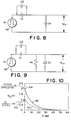
- FIG. 5 An equivalent circuit of the Fig. 4 short detection circuit 40 is shown in Fig. 5.
- C12 is very small, even when all of the nets of the circuit board electrically coupled to the being tested net are summed. Putting it differently, C12 is much smaller than either C1 or C2. Thus, C12 can be ignored. Consequently, the Fig. 5 circuit becomes that shown in Fig. 6.
- the dotted box represents UUT 14, and includes R12, C2 and C1.
- the resistance of R12 is at least about 1012 ohms.
- the responsive signal across C0 becomes an exponentially decaying waveform, as represented by the portion of the Fig.
- V c0 of Equation 2 is reflective of the value of a good net which may be obtained, for example, from predetermined product design values or determined empirically. For example, given the fact that the respective values of external capacitor C0 and the amplitude of input pulse V0 (i.e. leading edge 501) are known, a predetermined product design value of V c0 could be calculated by using Equation 2. Another approach is to determine V c0 empirically by measuring a number of good parts. Therefore, with reference to Fig. 7B, the value V c0 obtained from any being test net, as compared to its predetermined value, if found to be at point 53, would be considered a good net.
- any V c0 values across external capacitor C0 different from point 53 would not be a good net. Rather, such nets would be considered as either having an open, shorted to another net on the circuit board or has high leakage resistance to another net. As shown in Fig. 7B, once external resistor R0 comes into play, the voltage values across external capacitor C0 begin to decay, per downward slope waveform designated 52.
- a low leakage resistance As noted above, if the resistance separating the being tested net, for example net 16, and any other net on the circuit board, for example net 18, is small, there is a low resistance short, which may be referred to as a low leakage resistance.
- Equation 4 represents the situation where the being tested net, for example net 16, is shorted to any one of the nets, for example net 18, on the circuit board.
- the voltage value V c0 across C0 represented by Equation 4 is designated at point 54 in the graph of Fig. 10 and can be referred to in the instant invention as a "dead short". Putting it simply, the being tested net is determined to be directly shorted to another net on the circuit board.
- Equation 5 the exponential portion of Equation 5, represented by the waveform designated 56 in Fig. 10, takes on the time constant R0 (C1 + C2 + C0) .
- the amplitude (value) of the voltage across the external capacitor C0 would reflect whether the being tested net is a good net, completely shorted to some other net, or has a high leakage resistance to another net in the circuit board.
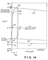
- Fig. 14 is a graph which has superimposed thereonto the respective waveforms of a good net, an open net, a dead short and a short with high leakage resistance.
- the waveforms of a good net, an opened net, a dead short and a high leakage resistance short are based on a predetermined value in accordance with the known values of external capacitor C0 and the value of input pulse V0.
- An opened net waveform is represented in Fig.
- portion 72 which represents the high leakage resistance between a being tested net and the net it is shorted to.
- the mathematical equation representing portion 58 is set forth in equation 6. where With reference to the graph of Fig. 14, the operation of the present invention system is as follows. Assume a predetermined value for a good net is at 60, and the threshold of what constitutes a dead short is above point 60 (such as point 64). To evaluate a net, a rectangular pulse that may have, for example a width of 200 ⁇ sec, is provided to the net, via generator 42 and probe 22 (see Fig. 4).
- transient digital analyzer 46 The response across external capacitor C0, as a waveform of discrete voltage values over time, is sampled by transient digital analyzer 46 and stored in a memory, such as memory 76M shown in Fig. 16.
- memory 76M shown in Fig. 16.
- the rectangular pulse being applied to the being tested net can also be used to stress test the same.
- the response across C0 would accordingly comprise a waveform, sampled (by transient digital analyzer 46) as a series of discrete voltage values through a 200 ⁇ sec period of time.
- the thus sampled values are recorded in memory 76M of the signal acquisition and digitizing system 76 (see Fig. 16).
- an evaluation is next made, based on a subportion of the recorded voltage values. For example, an of interest period such as 56 shown in Fig. 14 is evaluated to determine whether the rising edge 58 of the response signal waveform is sloping upwards; and if it is, it has high leakage resistance. The leakage resistance can be calculated from the initial slope. Using a different (later) subportion of the recorded voltage values, region 70, the combined - capacitance of the net under test and the net shorted to can be deduced. If the rising edge 58 of the response signal is sloping downwards, it is either a good net, dead short or an open net.
- the present invention system not only is capable of evaluating whether a being tested net is a "good net” or “dead short” to another net on the circuit board, it is also able to deduce the resistance between the being tested net and the net, if any, it is shorted to.
- the initial voltage amplitudes is dependant on the amplitude of the rectangular pulse and the sampling rate set in transient digital analyzer 46 (i.e. whether analyzer 46 is to measure 500, 600, or 700 etc. samples in the 200 ⁇ sec period of time discussed above).
- Fig. 16 The equipment utilized for the present invention system are illustrated in Fig. 16.
- the circuit under test (or UUT) 14 is connected to pulse generator 42.
- pulse generator 42 is a Berkeley Nucleonics Corp., BNC model 202H generator.
- Generator 42 is connected bi-directionally to a bus 73 to which there are also connected a system controller 74, a signal acquisition and digitizing system 76, and a trigger generator 78.
- System controller may be a conventional 486 type microprocessor.
- Signal acquisition and digitizing system 76 comprises at least one Analytek model 2000P transient digital analyzer, and includes a memory 76M.
- analyzers 36 and 46 shown in Fig. 3 are a part of signal acquisition and digitizing system 76.
- Connected to an input of system 76 are preamplifiers 80.
- System controller 74 controls the operations of system 76, trigger generator 78 and, to a certain extent, the operation of pulse generator 42 and transient digitizer 76, as well as analyzing the data to decide the integrity of the net being tested. In effect, controller 74 operations of trigger generator 78 and pulse generator 42 and transient digitizer 76 so that trigger pulses are generated from generator 78 to cause the transient digitizer 76 to start collecting data and pulse generator 42 to output a rectangular pulse 50, via a probe, for example 22 shown in Fig. 3, to a being tested net in circuit under test 14.
- the responsive signal (discrete voltage values as a function of time) across the external capacitor C0, designated 83, is provided to preamplifiers 80, before being fed to and stored in memory 76M.
- the leakage resistance can be calculated from the slope.
- the capacitance and resistance values can be calculated using Equations 7-12.
- the signal can either be displayed on an oscilloscope (not shown) or stored in memory (not shown) for later evaluation by the system controller or some means, if needed.
- current source 26 provides the current to the being tested net of circuit under test 14.
- the values of the voltage potentials are provided also to differential amplifiers 81 and recorded in memory 82M of digitizing system 82, as was discussed with respect to Fig. 3.
Landscapes
- Engineering & Computer Science (AREA)
- Computer Hardware Design (AREA)
- Microelectronics & Electronic Packaging (AREA)
- General Engineering & Computer Science (AREA)
- Physics & Mathematics (AREA)
- General Physics & Mathematics (AREA)
- Testing Of Short-Circuits, Discontinuities, Leakage, Or Incorrect Line Connections (AREA)
Applications Claiming Priority (2)
| Application Number | Priority Date | Filing Date | Title |
|---|---|---|---|
| US890910 | 1992-05-29 | ||
| US07/890,910 US5266901A (en) | 1992-05-29 | 1992-05-29 | Apparatus and method for resistive detection and waveform analysis of interconenction networks |
Publications (1)
| Publication Number | Publication Date |
|---|---|
| EP0572060A1 true EP0572060A1 (en) | 1993-12-01 |
Family
ID=25397324
Family Applications (1)
| Application Number | Title | Priority Date | Filing Date |
|---|---|---|---|
| EP93201310A Withdrawn EP0572060A1 (en) | 1992-05-29 | 1993-05-06 | Apparatus and method for resistive detection and waveform analysis of interconnection networks |
Country Status (3)
| Country | Link |
|---|---|
| US (1) | US5266901A (ja) |
| EP (1) | EP0572060A1 (ja) |
| JP (1) | JPH0766023B2 (ja) |
Cited By (2)
| Publication number | Priority date | Publication date | Assignee | Title |
|---|---|---|---|---|
| EP0862061A2 (en) * | 1997-02-28 | 1998-09-02 | Nidec-Read Corporation | Circuit board inspection apparatus and method |
| WO2004090560A2 (en) * | 2003-04-10 | 2004-10-21 | Colin Barker | Automatic test machine for testing printed circuit boards |
Families Citing this family (28)
| Publication number | Priority date | Publication date | Assignee | Title |
|---|---|---|---|---|
| US5402072A (en) * | 1992-02-28 | 1995-03-28 | International Business Machines Corporation | System and method for testing and fault isolation of high density passive boards and substrates |
| US5696451A (en) * | 1992-03-10 | 1997-12-09 | Hewlett-Packard Co. | Identification of pin-open faults by capacitive coupling |
| US5428300A (en) * | 1993-04-26 | 1995-06-27 | Telenix Co., Ltd. | Method and apparatus for testing TFT-LCD |
| US5486753A (en) * | 1993-07-30 | 1996-01-23 | Genrad, Inc. | Simultaneous capacitive open-circuit testing |
| US5432460A (en) * | 1994-01-03 | 1995-07-11 | International Business Machines Corporation | Apparatus and method for opens and shorts testing of a circuit board |
| US5438272A (en) * | 1994-05-09 | 1995-08-01 | International Business Machines Corporation | Voltage-stressing and testing of networks using moving probes |
| US5528137A (en) * | 1995-01-24 | 1996-06-18 | International Business Machines Corporation | Network sensitive pulse generator |
| US5596280A (en) * | 1995-06-15 | 1997-01-21 | International Business Machines Corp. | Apparatus and method for testing circuits by the response of a phase-locked loop |
| JP2994259B2 (ja) | 1996-03-28 | 1999-12-27 | オー・エイチ・ティー株式会社 | 基板検査方法および基板検査装置 |
| US6054863A (en) * | 1996-09-11 | 2000-04-25 | International Business Machines Corporation | System for testing circuit board integrity |
| JP3080595B2 (ja) * | 1997-02-28 | 2000-08-28 | 日本電産リード株式会社 | 基板検査装置および基板検査方法 |
| JP2001153921A (ja) * | 1999-11-29 | 2001-06-08 | Ando Electric Co Ltd | 波形観測治具および波形観測装置 |
| US6753688B2 (en) * | 2001-04-10 | 2004-06-22 | International Business Machines Corporation | Interconnect package cluster probe short removal apparatus and method |
| US6724210B2 (en) * | 2001-08-22 | 2004-04-20 | International Business Machines Corporation | Method and apparatus for reduced pin count package connection verification |
| US6573728B2 (en) | 2001-08-29 | 2003-06-03 | International Business Machines Corporation | Method and circuit for electrical testing of isolation resistance of large capacitance network |
| JP2004184385A (ja) * | 2002-11-30 | 2004-07-02 | Oht Inc | 回路パターン検査装置及びパターン検査方法 |
| WO2008091371A2 (en) * | 2006-07-18 | 2008-07-31 | Multiprobe, Inc. | Apparatus and method for combined micro-scale and nano-scale c-v,q-v, and i-v testing of semiconductor materials |
| JP5060499B2 (ja) * | 2009-02-10 | 2012-10-31 | マイクロクラフト株式会社 | プリント配線板の検査装置及び検査方法 |
| JP5420277B2 (ja) * | 2009-03-05 | 2014-02-19 | 日置電機株式会社 | 回路基板検査装置および回路基板検査方法 |
| JP4843071B2 (ja) * | 2009-06-04 | 2011-12-21 | マイクロクラフト株式会社 | プリント配線板の検査装置及び検査方法 |
| US8350583B2 (en) | 2009-08-12 | 2013-01-08 | International Business Machines Corporation | Probe-able voltage contrast test structures |
| JP5533169B2 (ja) * | 2010-04-13 | 2014-06-25 | 日本電産リード株式会社 | 検査装置 |
| US8399266B2 (en) | 2011-01-25 | 2013-03-19 | International Business Machines Corporation | Test structure for detection of gap in conductive layer of multilayer gate stack |
| US9780007B2 (en) | 2012-01-04 | 2017-10-03 | Globalfoundries Inc. | LCR test circuit structure for detecting metal gate defect conditions |
| JP5474114B2 (ja) * | 2012-03-16 | 2014-04-16 | 三菱電機株式会社 | 車載高電圧機器の漏電抵抗検出装置およびその漏電抵抗検出方法 |
| CN103063971B (zh) * | 2012-11-29 | 2015-11-25 | 惠州Tcl移动通信有限公司 | 一种钻孔检测电路及采用该钻孔检测电路的检测设备 |
| WO2017086948A1 (en) * | 2015-11-18 | 2017-05-26 | Intel Corporation | High power terahertz impulse for fault isolation |
| US10126350B2 (en) * | 2016-09-21 | 2018-11-13 | Hamilton Sunstrand Corporation | Detection of damper resistor degradation and failures |
Citations (4)
| Publication number | Priority date | Publication date | Assignee | Title |
|---|---|---|---|---|
| GB2136138A (en) * | 1983-03-07 | 1984-09-12 | Kollmorgen Tech Corp | Testing electrical interconnection networks |
| EP0196496A1 (en) * | 1985-04-01 | 1986-10-08 | International Business Machines Corporation | Printed circuit conductor test system |
| EP0246034A2 (en) * | 1986-05-16 | 1987-11-19 | AT&T Corp. | Method of testing electronic assemblies while they are being produced |
| WO1990004792A1 (en) * | 1988-10-17 | 1990-05-03 | Bath Scientific Limited | Testing electrical circuits |
Family Cites Families (4)
| Publication number | Priority date | Publication date | Assignee | Title |
|---|---|---|---|---|
| US4019129A (en) * | 1975-06-02 | 1977-04-19 | Bell Telephone Laboratories, Incorporated | Metallic plating testing apparatus |
| NO165697C (no) * | 1988-03-10 | 1991-03-20 | Inter Marketing Oy Ab | Sensor for ekthetskontroll av sikkerhetspapir. |
| US5006808A (en) * | 1989-03-21 | 1991-04-09 | Bath Scientific Limited | Testing electrical circuits |
| US5138266A (en) * | 1989-10-20 | 1992-08-11 | Digital Equipment Corporation | Single-probe charge measurement testing method |
-
1992
- 1992-05-29 US US07/890,910 patent/US5266901A/en not_active Expired - Fee Related
-
1993
- 1993-04-23 JP JP5098143A patent/JPH0766023B2/ja not_active Expired - Lifetime
- 1993-05-06 EP EP93201310A patent/EP0572060A1/en not_active Withdrawn
Patent Citations (4)
| Publication number | Priority date | Publication date | Assignee | Title |
|---|---|---|---|---|
| GB2136138A (en) * | 1983-03-07 | 1984-09-12 | Kollmorgen Tech Corp | Testing electrical interconnection networks |
| EP0196496A1 (en) * | 1985-04-01 | 1986-10-08 | International Business Machines Corporation | Printed circuit conductor test system |
| EP0246034A2 (en) * | 1986-05-16 | 1987-11-19 | AT&T Corp. | Method of testing electronic assemblies while they are being produced |
| WO1990004792A1 (en) * | 1988-10-17 | 1990-05-03 | Bath Scientific Limited | Testing electrical circuits |
Cited By (4)
| Publication number | Priority date | Publication date | Assignee | Title |
|---|---|---|---|---|
| EP0862061A2 (en) * | 1997-02-28 | 1998-09-02 | Nidec-Read Corporation | Circuit board inspection apparatus and method |
| EP0862061A3 (en) * | 1997-02-28 | 2000-02-02 | Nidec-Read Corporation | Circuit board inspection apparatus and method |
| WO2004090560A2 (en) * | 2003-04-10 | 2004-10-21 | Colin Barker | Automatic test machine for testing printed circuit boards |
| WO2004090560A3 (en) * | 2003-04-10 | 2005-01-20 | Colin Barker | Automatic test machine for testing printed circuit boards |
Also Published As
| Publication number | Publication date |
|---|---|
| JPH0766023B2 (ja) | 1995-07-19 |
| JPH06109796A (ja) | 1994-04-22 |
| US5266901A (en) | 1993-11-30 |
Similar Documents
| Publication | Publication Date | Title |
|---|---|---|
| US5266901A (en) | Apparatus and method for resistive detection and waveform analysis of interconenction networks | |
| US5254953A (en) | Identification of pin-open faults by capacitive coupling through the integrated circuit package | |
| US6111414A (en) | System, circuit, and method for testing an interconnect in a multi-chip substrate | |
| Gulski et al. | PD measurements on-site using oscillating wave test system | |
| US5138266A (en) | Single-probe charge measurement testing method | |
| US7075307B1 (en) | Method and apparatus for detecting shorts on inaccessible pins using capacitive measurements | |
| US20150142344A1 (en) | Method and apparatus for measuring partial discharge charge value in frequency domain | |
| EP0840227A1 (en) | Method and apparatus for determining IDDQ | |
| Ward | Digital techniques for partial discharge measurements | |
| US5438272A (en) | Voltage-stressing and testing of networks using moving probes | |
| US4517511A (en) | Current probe signal processing circuit employing sample and hold technique to locate circuit faults | |
| Montanari et al. | Random sampling and data processing for PD-pulse height and shape analysis | |
| US5432460A (en) | Apparatus and method for opens and shorts testing of a circuit board | |
| EP2425265B1 (en) | System and method for detecting sensor leakage | |
| US4063168A (en) | Method and apparatus for locating the source of corona discharge | |
| EP0052290A1 (en) | Cable break locator | |
| JP2004264147A (ja) | 静電気試験装置 | |
| Kolev et al. | Development of partial discharge model, simulation and measurement | |
| Riad et al. | Application of the homomorphic deconvolution for the separation of TDR signals occurring in overlapping time windows | |
| Hyatt et al. | Charged device model (CDM) metrology: limitations and problems | |
| JP3246679B2 (ja) | 絶縁体の絶縁特性測定装置 | |
| EP0077725A1 (en) | Current probe signal processing circuit | |
| Jenkins et al. | Measurement of VLSI power supply current by electron-beam probing | |
| JPH11211772A (ja) | 電力機器のインパルス試験方法 | |
| Henry et al. | Charged device model metrology: limitations and problems |
Legal Events
| Date | Code | Title | Description |
|---|---|---|---|
| PUAI | Public reference made under article 153(3) epc to a published international application that has entered the european phase |
Free format text: ORIGINAL CODE: 0009012 |
|
| AK | Designated contracting states |
Kind code of ref document: A1 Designated state(s): DE FR GB |
|
| 17P | Request for examination filed |
Effective date: 19940324 |
|
| STAA | Information on the status of an ep patent application or granted ep patent |
Free format text: STATUS: THE APPLICATION IS DEEMED TO BE WITHDRAWN |
|
| 18D | Application deemed to be withdrawn |
Effective date: 19961203 |