EP0569718B1 - Method and apparatus for reading data - Google Patents
Method and apparatus for reading data Download PDFInfo
- Publication number
- EP0569718B1 EP0569718B1 EP93105995A EP93105995A EP0569718B1 EP 0569718 B1 EP0569718 B1 EP 0569718B1 EP 93105995 A EP93105995 A EP 93105995A EP 93105995 A EP93105995 A EP 93105995A EP 0569718 B1 EP0569718 B1 EP 0569718B1
- Authority
- EP
- European Patent Office
- Prior art keywords
- data
- track
- track center
- disk
- optical
- Prior art date
- Legal status (The legal status is an assumption and is not a legal conclusion. Google has not performed a legal analysis and makes no representation as to the accuracy of the status listed.)
- Expired - Lifetime
Links
Images


Classifications
-
- G—PHYSICS
- G11—INFORMATION STORAGE
- G11B—INFORMATION STORAGE BASED ON RELATIVE MOVEMENT BETWEEN RECORD CARRIER AND TRANSDUCER
- G11B7/00—Recording or reproducing by optical means, e.g. recording using a thermal beam of optical radiation by modifying optical properties or the physical structure, reproducing using an optical beam at lower power by sensing optical properties; Record carriers therefor
- G11B7/12—Heads, e.g. forming of the optical beam spot or modulation of the optical beam
- G11B7/13—Optical detectors therefor
- G11B7/131—Arrangement of detectors in a multiple array
-
- G—PHYSICS
- G11—INFORMATION STORAGE
- G11B—INFORMATION STORAGE BASED ON RELATIVE MOVEMENT BETWEEN RECORD CARRIER AND TRANSDUCER
- G11B7/00—Recording or reproducing by optical means, e.g. recording using a thermal beam of optical radiation by modifying optical properties or the physical structure, reproducing using an optical beam at lower power by sensing optical properties; Record carriers therefor
- G11B7/08—Disposition or mounting of heads or light sources relatively to record carriers
- G11B7/09—Disposition or mounting of heads or light sources relatively to record carriers with provision for moving the light beam or focus plane for the purpose of maintaining alignment of the light beam relative to the record carrier during transducing operation, e.g. to compensate for surface irregularities of the latter or for track following
- G11B7/0901—Disposition or mounting of heads or light sources relatively to record carriers with provision for moving the light beam or focus plane for the purpose of maintaining alignment of the light beam relative to the record carrier during transducing operation, e.g. to compensate for surface irregularities of the latter or for track following for track following only
-
- G—PHYSICS
- G11—INFORMATION STORAGE
- G11B—INFORMATION STORAGE BASED ON RELATIVE MOVEMENT BETWEEN RECORD CARRIER AND TRANSDUCER
- G11B7/00—Recording or reproducing by optical means, e.g. recording using a thermal beam of optical radiation by modifying optical properties or the physical structure, reproducing using an optical beam at lower power by sensing optical properties; Record carriers therefor
- G11B7/12—Heads, e.g. forming of the optical beam spot or modulation of the optical beam
- G11B7/125—Optical beam sources therefor, e.g. laser control circuitry specially adapted for optical storage devices; Modulators, e.g. means for controlling the size or intensity of optical spots or optical traces
- G11B7/127—Lasers; Multiple laser arrays
-
- G—PHYSICS
- G11—INFORMATION STORAGE
- G11B—INFORMATION STORAGE BASED ON RELATIVE MOVEMENT BETWEEN RECORD CARRIER AND TRANSDUCER
- G11B7/00—Recording or reproducing by optical means, e.g. recording using a thermal beam of optical radiation by modifying optical properties or the physical structure, reproducing using an optical beam at lower power by sensing optical properties; Record carriers therefor
- G11B7/12—Heads, e.g. forming of the optical beam spot or modulation of the optical beam
- G11B7/125—Optical beam sources therefor, e.g. laser control circuitry specially adapted for optical storage devices; Modulators, e.g. means for controlling the size or intensity of optical spots or optical traces
- G11B7/128—Modulators
-
- G—PHYSICS
- G11—INFORMATION STORAGE
- G11B—INFORMATION STORAGE BASED ON RELATIVE MOVEMENT BETWEEN RECORD CARRIER AND TRANSDUCER
- G11B7/00—Recording or reproducing by optical means, e.g. recording using a thermal beam of optical radiation by modifying optical properties or the physical structure, reproducing using an optical beam at lower power by sensing optical properties; Record carriers therefor
- G11B7/12—Heads, e.g. forming of the optical beam spot or modulation of the optical beam
- G11B7/135—Means for guiding the beam from the source to the record carrier or from the record carrier to the detector
- G11B7/1362—Mirrors
-
- G—PHYSICS
- G11—INFORMATION STORAGE
- G11B—INFORMATION STORAGE BASED ON RELATIVE MOVEMENT BETWEEN RECORD CARRIER AND TRANSDUCER
- G11B7/00—Recording or reproducing by optical means, e.g. recording using a thermal beam of optical radiation by modifying optical properties or the physical structure, reproducing using an optical beam at lower power by sensing optical properties; Record carriers therefor
- G11B7/12—Heads, e.g. forming of the optical beam spot or modulation of the optical beam
- G11B7/135—Means for guiding the beam from the source to the record carrier or from the record carrier to the detector
- G11B7/1384—Fibre optics
-
- G—PHYSICS
- G11—INFORMATION STORAGE
- G11B—INFORMATION STORAGE BASED ON RELATIVE MOVEMENT BETWEEN RECORD CARRIER AND TRANSDUCER
- G11B7/00—Recording or reproducing by optical means, e.g. recording using a thermal beam of optical radiation by modifying optical properties or the physical structure, reproducing using an optical beam at lower power by sensing optical properties; Record carriers therefor
- G11B7/12—Heads, e.g. forming of the optical beam spot or modulation of the optical beam
- G11B7/14—Heads, e.g. forming of the optical beam spot or modulation of the optical beam specially adapted to record on, or to reproduce from, more than one track simultaneously
Definitions
- the present invention relates to optical disks. More particularly, the invention relates to a method and apparatus for reading large amounts of data at a high rate from optical disks.
- Optical disks are becoming the base for computerized archives and data bases because of their huge capacity. When they are organized in a jukebox which contains tens of disks and numerous disk drivers, they can form very large archives.
- the main disadvantage of these disks and disk system is the serial mode in which the data is read from them. Coupled with slow access time this mode limits the search performance and the rate at which the data is transferred to the computing system.
- An optical disk contains an index of the data. By using the index, the access time to a piece of data is shorter than if the data has to be searched for serially.
- the index is of no help and searching through all the disk is required.
- Optical disks of various kinds are based on concentric circular or spiral tracks on which the data is written in the form of spots of changes of some optical property of the disk media. These changes are typically spots of higher reflection than the non data-containing parts of the disk. These data spots lie along a spiral or circular path on the disk.
- the disk is divided into sectors, and each loop of this spiral path that lies within a sector is called a track.
- the data is read from the optical disk by an electro-optical head which projects a narrow light spot on the rotating disk, reads the reflected light from the disk and transduces it into an electrical signal. At any point in time the head reads one spot of data. By rotating the disk below the head, a track is read spot by spot. To read data from outer or inner tracks, the head is moved to the desired track by a motor. In advanced split head design the moving head is composed of a lens, a focusing coil motor, a fine tracking motor and mirrors. This combination of rotating disk with a radially moving head enables to access any data spot on the disk.
- the reading of the data spots is done serially along a track or along the whole spiral path.
- Commercially available optical disks have internal data transfer rates of about 15 Mbit/sec, which translates to an output rate of 1.25 Mbyte/sec. Searching through a whole disk may thus take more than ten minutes.
- Optical heads can read several tracks simultaneously when combining a lens with a wide field of view and a matrix of light detectors that cover this field. Processing the signal from each of these detectors separately, in parallel, multiplies the data throughout proportionately to the number of detectors.
- a matrix of detectors is described, e.g., in US 5,111,445.
- implementing parallel reading of an optical disk by a detector matrix requires first solving some severe problems.
- the first problem is that of sampling the data spots that lie on a polar coordinate system by a matrix of detectors set in a rectangular coordinate system. As a result of such sampling, data spots may be sampled not in track order, which may result in the scrambling of the data structure.
- Another problem is that unlike the electro-optical head according to the known art, which has a servo system to center the head over the track, centering a line-scan matrix over many curved tracks is very difficult. Without centering the detectors on the tracks, radial movement of the disk may shift the data spots between neighboring detectors and thus, again, scramble the data structure. All of this has to be done at the very fast speed of the data spots (i.e., 15 Mbit/sec.).
- Yet another problem is that a detector matrix cannot economically cover all the tens of thousands of tracks, so that some means for fast moving to different group of tracks is needed. After each of such movement the detector matrix have to be aligned to the right tracks.
- Belgian Patent No. 831,264 describes an optical disk reading system including a laser light emitter that emits an elongated beam of light that encompasses multiple data tracks, and a sensor comprising a multiplicity of light sensitive elements that generate signals corresponding to information stored on in the data tracks.
- electronic logic may be provided to detect and correct for shifting in the track centers caused by eccentricity of the data tracks.
- reading data from an optical disk requires high precision. Ordinarily, such a reading is carried out using coherent light, even if writing of the data has been effected with non-coherent light, e.g., as in US 3,805,275 or US 4,135,251. In some instances non-coherent light has been used in illuminating data in the form of the amplitude-modulation of the relief height of a pattern of surface relief variation, such as in the microfiche-like system described in US 4,486,870. However, such systems cannot read multitrack information and require the use of precise and expensive servo mechanisms.
- the present invention is directed to the use of a non-coherent optical system for carrying out fast data reading from an optical disk, without the use of a mechanical servo mechanism for small position corrections. While the invention comprises many different aspects, it should be understood that in each case the two aforementioned characteristics are maintained, viz., a non-coherent system is used and no mechanical servo mechanism is provided for correcting local drift. It should be understood that the ability of fast addressing the data on the optical disk, with high precision, is related to the fact that an electronic servo mechanism is employed, and is made possible by the use of a non-coherent system in a manner never devised before in the art.
- the reading device for an optical data disk comprises an optical apparatus for fast addressing tracks on the disk, optical apparatus for imaging the tracks on detector matrix comprising a plurality of detectors arranged in parallel lines, the said detector matrix being coupled to a plurality of shift registers, whereby electric charge generated by light falling on each cell is transferred to the following cell and the shift register receives the combined charge from the last cell in the line.
- One such device is the so-called TDI sensor, described, e.g. in D.F. Barbe, “Time delay and integration image sensors", Solid State Imaging, P.G. Jespers et al, Nordhoff, The Netherlands, pp. 659-671 (1976).
- the device according to the invention further comprises image processing means to receive the image generated by the detector matrix and to translate said image into data contained in data spots located on the disk.
- the invention is further directed to a method of accessing and reading data from an optical disk, which method comprises the steps of:
- the method is characterized in that the light omitted from the means for illuminating is non-coherent.
- the method further comprises the steps of analyzing the output signal of the detector matrix to determine position coordinates of the track center for each data track; of saving in memory means expected track center data, comprising position coordinates of the track center located by the step of analyzing the output signal; and, if an actually detected track center is shifted with respect to the said expected track center, of electronically moving the track center position.
- the method further comprises a step of electronically accessing neighboring tracks via operation of a multiplexer unit.
- the method further includes the steps of carrying out a "locking" operation to determine the track center coordinastes; and of using the coordinated of the track center so determined as a first reference value for the expected track center.
- the method may optionally further include a step of storing a number of consecutively determined track center values for each track center.
- the method may also include a step of locating a track position for one of the plurality of tracks; and, determining the length of the data segments within that track.
- the method may include a step of subtracting each pixel from its cross-track neighbor, or the steps of subtracting each pixed from its along track neighbor to generate a first difference; and of subtracting the first difference in the cross track direction.
- the step of determining the length of the data segments may be carried out by means of convoluting the optical image of the data with an edge detection operator, said edge detection operator being the difference of two Gaussians.
- the convolution operator is of varying kernel length, utilizing short kermel at high dense areas, and longer kernels at less dense areas.
- An additional step of applying a preprocessing (PPD) filter to the data may also be included.
- PPD preprocessing
- the invention also relates to an apparatus for reading an optical disk for the embodiment of said method.
- Said apparatus comprising means for illuminating that illuminates a portion of the optical disk; and a detector matrix comprising a plurality of detectors arranged in parallel lines, the detector matrix receiving an optical image corresponding to reflected illumination from the optical disk, the detector matrix being coupled to a plurality of shift registers, whereby an electric charge generated by reflected illumination incident on each detector is summed with the charge generated by reflected illumination incident on previous detectors and transferred at the disk rotating speed to the following detector, the shift register receiving the charge from the last detector in the column.
- the apparatus is characterized in that the means for illuminating emit non-coherent light.
- the apparatus further comprises a multiplexer unit that electronically accesses neighboring tracks, image processing means that receive signals generated by the detector matrix and translate the signals into information corresponding to data sports located on the optical disk.
- a so-called "locking" operation is carried out, to determine the track center, and the coordinates of the track center initially found are used as the first value for the expected track center. Additionally, in another preferred embodiment of the invention a number of track center values consecutively determined are considered, to permit statistical evaluation of drift and other system parameters.
- the ability to move to the centers of the data tracks electronically, by redefining the position of said tracks without the need for mechanical adjustment, enables the compensation for small drift in the disk movement. This compensation is critical for reading many tracks simultaneously. This ability to compensate quickly for such drift is one important feature of the invention, which permits to process large amounts of data at high rates.
- coherent systems require that the phase of the electromagnetic wave be taken into account, while non-coherent systems only accumulate the level of the signal generated by the light they detect. It has been found, and this is an aspect of the invention, that the use of non-coherent systems permits to avoid many drawbacks found in prior art systems utilizing coherent light and imaging systems. For instance, edges are sharp in coherent systems and lead to overshoot and undershoot effects in the detected signal, which do not exist in non-coherent systems. Furthermore, because coherent systems are phase-dependent, every factor which influences the phase, such as changes in height or slope of the optical surface, affect the data read from the disk. Thus, for instance, prior art parallel read systems are very sensitive to dust and dirt.
- the system of the invention is much less sensitive to irregularities of the optical medium and is therefore much less disturbed by dust and dirt.
- the invention is directed to a method which permits to reduce the adverse effect of irregularities on the surface of the optical media and thus to increase the accuracy of readings therefrom.
- the ability to scan the disk without moving the optical head, but only lightweight optics is also another important feature. Another important feature is the ability to access data tracks electronically, within close proximity.
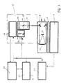
- Fig. 1 the preferred embodiment of the system for disk searching and reading is described.
- An optical disk 2 to be scanned by the system is placed in optical disk driver 4 which rotates the disk.
- Above disk 2 there is relay optics unit 6 that images the disk to intermediate image above it.
- the relay optics has a long optical path.
- the data is acquired by one or more reading heads 12, each one comprises of microscope 10, light source 16 and detector matrix 14. These units are to be described below.
- the disk is illuminated by a light beam that is emitted from light unit 16, focused by microscope 10 and relayed by relay optics 6 to generate a uniform area of non-coherent illumination on disk 2.
- the light unit 16 is composed of a laser diode or a laser diode array, a fiber optics (both not shown), and a projection lens which projects the light onto the back focal plane of the objective lens such that the full aperture of the objective is illuminated.
- the disk is illuminated with the full numerical aperture of the objective.
- This provides for a non-coherent system. This systems is particularly convenient, as will be apparent to the skilled person, when used in conjunction with a TDI.
- the light reflected from the disk is relayed by relay optics 6 to form an image of the disk inside the microscope 10, said image being re-imaged by microscope 10 on detector matrix 14.
- the electrical signal that is generated by detector matrix 14 is processed by signal processing module 20.
- This module detects the presence and location of the sets of data spots.
- Data spots information is sent to storage module 22 and after structuring, the data is sent to a computer system (not shown).
- the data spot location signal is sent to controller 24.
- the controller sums up the changes in data spot location on the tracks and sends correction signals to signal processor 20.
- Controller 24 sends also synchronization signals to detector matrix 14, to signal processor 20, and to storage module 22.
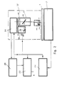
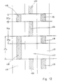
- the preferred embodiment of the relay optics is of two spherical mirrors arranged in Offner telecentric type ["Offner 1:1 system: some further uses", M.V.R.K. Murtz. Optical Engineering, Vol. 24, No. 2, pp. 326-328 (April, 1985), Offener, USP 3,748,015].
- the light from the disk is folded by mirror 102 toward spherical mirror 104.
- the light is reflected from mirror 104 toward the second spherical mirror 106 that reflects the light back to mirror 104.
- the reflected light from mirror 104 is folded by mirror 108 toward the microscope 10.
- Microscope 10 consists of objective lens 118, beam splitter 120 and tube lens 122.
- the objective lens is, for example, of X25 magnification (together with the tube lens) and the beam splitter is of 50:50 ratio.
- the beam splitter 120 By replacing the 50:50 beam splitter 120 with a polarizing beam splitter and inserting a ⁇ /4 plate between the beam splitter and the objective lens, and by replacing mirror 128 with a polarizing mirror, the system becomes sensitive to polarization, which is an important factor for some types of optical disks.
- the light from light source 124 is focused by lens 126 in the back focal plane of objective lens 118, to form a Kohler illuminating system.
- Mirror 128 folds the light toward beam splitter 120 so that it folds it toward objective lens 118.
- the light is relayed by relay optics 6 toward disk 2 in order to generate uniform areas of light on it.
- a light split head for the sake of brevity, the relay optics is left out and the objective lens 118 is set directly above the optical disk.
- the focusing of the microsccpe is done by voice coil 116, which moves objective lens 118 towards the disk according to the focusing signal from focusing sensor 18.
- the objective lens 118 and its voice coil 116 are moved directly by a motor to image the required tracks of the disk by microscope 10.
- This embodiment is simpler but still faster than a conventional split head, since the fine tracking coil is eliminated due to the use of electronic tracking, thereby significantly reducing the weight of the moving parts.
- a plurality of disks can also be provided, each having its own drive or mounted on a single spindle where each disk has its own moving part 117.
- the structure of the detector matrix 14, the organization of the signal processing unit 20, the storage module 22 and the controller unit 24 are designed to solve the problems described above in parallel reading of data in an optical disk by a rectangular matrix of detectors. Also, they are designed to detect and register the data spots on their data track at the fast rate at which the data spots are passing by the detectors.
- the detector matrix is of the CCD type, and is organized in a TDI (Time Delay and Integration) structure.
- the TDI detector matrix 14 includes a plurality of parallel lines 34 through n, each of which contains a large number of detectors.
- the electrical charge generated by the light falling on each detector in the lines 34 can be transferred to the neighboring detector of the adjacent line of detectors, and be summed with the charge of the neighboring detector 36.
- the transfer of charge from one line of detectors is synchronized with the movement of the data spot along the detectors columns 38.
- the speed of transfer of the charges is therefore equal to the tangential velocity of the disk.
- the charges generated by a moving data spot on the detectors that lie on one of the columns 38 are summed by this transfer to give a stronger signal at the last line, n.
- the charge from the last row n is transferred to a readout shift registers 44.
- Each shift register 44 is connected to a segment of the last row of detectors, n, and the charge from the detectors of the segment is transferred thereto.
- the charge from each cell of the shift register is read out serially.
- the readout data rate from the shift registers 44 limits the transfer rate of charges from row to row. Therefore, the number of detectors connected to each shift register should fit the required readout rate and the detector transfer rate. For example, for a disk with a data rate of 15 Mspot/sec. and a CCD detector with an output transfer rate of 60 Mhz, each shift register is connected to four detectors.
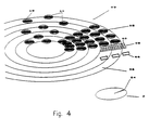
- Fig. 4 illustrates the relation between the illuminated area on the disk and the image on the detector matrix 14.
- the magnified image 53 of the illuminated area 54 on the disk 2 lies over the detectors 58 of the detector matrix 14 so that the images of the data spots 52 on tracks 56 of the rotating disk 2 are crossing the last row of detectors perpendicularly. Due to diffraction, the diameter of the image spot is approximately equal to the width of the track.
- each image of data spot 52 lies over a square that contains nXm detectors.
- This nXm sampling of a data spot enables to localize a data spot on the right track when the disk has a small radial movement. It also enables to detect the presence of two succeeding data spots that are barely resolved, in inner tracks of the disk.
- the number of detectors along a column 60 is limited by the curvature of the tracks 56 on the disk.
- the shift in the horizontal position of a track between the first row and the last row is less than a tenth of the size of a detector, for an inner track (at a radius of 3 cm). The difference between the tangential velocity of a data spot on the first and the last row is negligible.
- the tracks can be shifted with large amplitude.
- the rows of detectors have to be long enough to "see” the shifted tracks as well.
- additional 2.w/ (d/m) detectors should be provided in the detector matrix 14. Alternatively, only small and fast shifts are compensated for electronically, and large slow shifts are mechanically compensated.
- the transfer rate of rows is about 15 Mrows/sec.
- the required data rate is then 320 Mbit/sec.
- 320/ (15/3) 64 spots must be read in parallel.
- the total number of detectors will be 312. If each four detectors are connected to a shift register, the number of shift registers required will be at least 78.
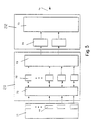
- Fig. 5 schematically illustrates image processing module 20.
- the module receives signals from detector matrix unit 14.
- the data from each shift register 44 of detector matrix 14 is fed to input memory buffers 70.
- Input memory buffers 70 are connected to a set of track processors (TP) 72 that detect the presence of image spots.
- TP track processors
- the input memory buffer can also serve as a multiplexing unit transferring only a section of the detector outputs into the processors. By switching electronically between different sections of the matrix, a fast access to neighboring tracks is available.
- Track detectors 72 align the spots on their right tracks. This alignment is done locally for small radial movement of the disk. More global alignment is done by system controller 24.
- the TPs are connected via a multiplexer unit 73 (Fig. 5) to a set of error detection and correction (EDC) units 74.
- EDC error detection and correction
- the EDC units are designed to extract and correct the data and store the segment data until it is ready for output.
- the output data is stored segment by segment in output frame buffer 75, where they are grouped to 8 bit byte.
- the EDC units 74 need to work at the rate of about 320 Mbit/sec, if a factor of at least 2 in detection/correction and header data, and 8 bits per byte are assumed. This requires about nine such units if each unit can process data at 20 Mhz.
- TP units 72 now need to process about 9 pixels for each output bit. This means that the system effective rate in pixel processing is 2880 Mpixels/sec. Such a rate is possible if 64 such units are used.
- the units are timed so that the interaction between TP 72, EDC 74 and the output buffer is synchronized.
- Track processor 72 works in three modes: 1) detecting; 2) tracking and 3) locking. In the detection mode, a spot 52 or a string of spots are identified by means of edge detection.
- DOG Gaussians
- G" (x) (1-x 2 /2 ⁇ 2 ) . e -(x 2 /2 ⁇ 2 )
- the edge detection method is used in the context of the invention, and as such also forms a part of the invention.
- the DOG operator 300 is one-dimensional, and in the preferred embodiment of the invention its size is of odd number, is referred to as the "kernel" and is comprised of center and the right and left shoulders.
- the DOG operator 300 is applied to the data along the track.
- the convolution operation yields a convolved image comprising an array of positive, negative and zero values.
- the edges position is represented by the zero-crossing between adjacent positive and negative values.
- the location of the zero-crossing is calculated in sub-pixel accuracy, using interpolation.
- the accuracy of the edge detector is very high as long as only one edge is located within the scope of the said operator.
- the said operator is designed to compute the location of the edge which is currently nearest to the said operator's center, which is the edge of interest. If other edges reside within the scope of the said operator, they bias the calculations designated to determine the position of the edge of interest.
- a special algorithm is applied to the raw data to dramatically reduce the influence of non-relevant edges residing within the scope of the DOG operator. This algorithm, the Pre-Processor for the DOG (PPD) operator 300, processes the raw data before the said operator is applied to it.
- the PPD identifies the change in intensity, above a given threshold, which is nearest to the center of the kernel, and assumes it represents the edge of interest. The direction of the intensity of the edge of interest is then determined. All other changes in intensity (if such exist), above another given threshold, and in opposite direction to the edge of interest, are taken to be irrelevant edges.
- the algorithm inspects each shoulder sequentially, from the center out. Pixels that form an edge with the preceding pixel, and the direction of the edge intensity is opposite to the direction of the intensity of the edge of interest, are set to the value of the preceding pixel. If the direction of the intensity is the same as that of the edge of interest, no action is taken. If no irrelevant edges are detected, no action is taken.
- the following example illustrates the actions taken by the PPD.
- the center of the kernel is placed over pixel 322 and is left of the edge 308, which position is to be calculated.
- the kernel in this example is nine pixels wide.
- the PPD is searching the data on the right hand side of the kernel, sequentially.
- Edge 310 having an intensity gradient in the same direction as that of edge 308, is left as is.
- Edge 312 having an intensity gradient in the opposite direction than that of edge 308, is eliminated by setting pixel 326 to the value of pixel 324.
- pixel 328 which is also set to the value of pixel 324, eliminating edge 314.
- edge 306 is left as is, having an intensity gradient in the same direction as that of edge 308.
- Edge 318 having an intensity gradient in the opposite direction than that of edge 308, is eliminated by setting the value of pixel 334 to the value of pixel 332.
- the "cleaner" data segment as submitted to the convolution operator, is illustrated.
- the values of pixels 326 and 328 are now leveled with the value of pixel 324.
- Pixel 334 has now the same value as pixel 332. Edges 312, 314 and 318 have been eliminated.
- Another embodiment of the PPD method includes a varying size kernel where a short kernel is executed at highly dense areas and a long kernel is executed at sparse areas.
- the distance between adjacent edges is computed and translated into "spot" units. This translation is dependent on the overlap ratio between spots and the radial distance of the given track from the rotational axis of the disk.
- TP 72 In the locking mode, the initial location of the center of the track is computed and set. TP 72 calculates the half-width distance between two of the nearest successive tracking spots 64 (in Fig. 4) of the sector header, and confirms this with the timing spot(s) 68 on the track center.
- the sampling resolution is three pixels across each track.
- the maximum (or minimum) value across the track (over 4 pixels) is computed in sub-pixel resolution. The location of the maximum is recorded. This process is referred to as the "peak detection". Any shift in the position of the maximum, relative to the current track center, is detected. The new track center is computed and the corresponding pixel nearest the center of the track is tagged as the central pixel of the track. For non-sampled tracks, where the tracking points do not exist, the locking is performed on the track data.
- the edges of a spot or a string of spots are detected, along the track direction.
- the distance between adjacent edges is computed at the center of the track.
- the above distance is translated into "spot" units, taking into account the overlap between the spots and the radial distance of the given track from the rotational axis.
- the distance between adjacent strings of spots is computed. The length of the strings and the gaps between them are then used by the decoding schemes.
- the peak detection mechanism is quite similar to the edge detection mechanism, "peak location” meaning the location along a row of pixels across a track and between two track edges, where the maximum (or minimum) intensity value is located.
- the operator used for the peak detection is the First Difference operator 400, which is a one-dimensional operator consisting of two values: +1 and -1. Convolving the operator with pixels across the track direction, yields a convolved image comprising an array of positive, negative and zero values. The zero-crossing between adjacent positive and negative values represent points of maxima and minima of the intensity levels. The gradient direction of the zero-crossing determines whether it is a minimum or a maximum. The exact position of each zero crossing is again computed in a sub-pixel accuracy, using interpolation. To reduce high-frequency noise it is possible to convolve the image with a one-dimensional Gaussian mask, across the tracks, before applying the First Difference operator.
- Reading the picture from a conventional optical disk, having an addressing time of 70 msec, and a data reading rate of 1.25 Mbyte/sec, requires a time of: [ 6 MByte / (1.25 Mbyte/sec) ] + 0.07 sec 4.87 sec.
- the invention permits the reading of such a picture at a speed greater by one order of magnitude.
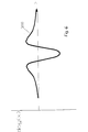
- Pixel 452 represents the difference between pixels 442 and 444 and thus is located in space exactly between them. It has a value of 40. Similarly, Pixel 454 has a value of 30, Pixel 456 has a value of -70.
- the zero cross lies between pixels 454 and 456, viz., within Pixel 446.
- the minimum is located at pixel 446, 0.3 pixel from its left boundary.
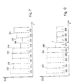
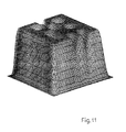
- Fig. 11 shows the simulation of a segment of the tracks.
- Fig. 12 gives an overview of Fig. 11.
- Table 1 is the conversion of this image into digitized values. First we determine which column of pixels in each track represents the track data center.
- Applying the First Difference operator 400 produces the array of values given in Table 2.
- the position of the zero-crossings are now computed, where values between two adjacent columns are changing from negative to positive.
- a 1:3 linear interpolation is used in this example, resulting in the array shown in Table 3.
- a value of 1 in the said table represents the center of the data in its track. In this example, columns 5, 8 and 10 were selected. Once the center of each track was determined, the data itself was identified.
- the DOG operator 300 was applied to the same data given in Table 1, with a kernel width of five.
- the array of values given by Table 4 is produced. Now, zero-crossings are searched for along each center track, as determined in the tracking mode (columns 5, 8 and 10). Again, a 3:1 linear interpolation is applied to determine the edge location, resulting in the array shown in Table 5.
Landscapes
- Physics & Mathematics (AREA)
- Optics & Photonics (AREA)
- Optical Recording Or Reproduction (AREA)
- Radar Systems Or Details Thereof (AREA)
- Inspection Of Paper Currency And Valuable Securities (AREA)
- Optical Head (AREA)
Applications Claiming Priority (2)
| Application Number | Priority Date | Filing Date | Title |
|---|---|---|---|
| IL101570 | 1992-04-10 | ||
| IL101570A IL101570A0 (en) | 1992-04-10 | 1992-04-10 | Method and apparatus for reading data |
Publications (3)
| Publication Number | Publication Date |
|---|---|
| EP0569718A2 EP0569718A2 (en) | 1993-11-18 |
| EP0569718A3 EP0569718A3 (OSRAM) | 1994-01-05 |
| EP0569718B1 true EP0569718B1 (en) | 1999-08-25 |
Family
ID=11063542
Family Applications (1)
| Application Number | Title | Priority Date | Filing Date |
|---|---|---|---|
| EP93105995A Expired - Lifetime EP0569718B1 (en) | 1992-04-10 | 1993-04-13 | Method and apparatus for reading data |
Country Status (5)
| Country | Link |
|---|---|
| US (5) | US5426623A (OSRAM) |
| EP (1) | EP0569718B1 (OSRAM) |
| AT (1) | ATE183845T1 (OSRAM) |
| DE (1) | DE69326096T2 (OSRAM) |
| IL (1) | IL101570A0 (OSRAM) |
Families Citing this family (72)
| Publication number | Priority date | Publication date | Assignee | Title |
|---|---|---|---|---|
| IL101570A0 (en) * | 1992-04-10 | 1992-12-30 | Amir Alon | Method and apparatus for reading data |
| US5825743A (en) * | 1993-04-06 | 1998-10-20 | Zen Research N.V. | Illuminating multiple data tracks of an optical disk with a laser source of reduced coherence |
| IL106009A0 (en) * | 1993-06-14 | 1993-10-20 | Amir Alon | Method and apparatus for the simultaneous writing of data on an optical disk |
| IL107181A0 (en) * | 1993-10-04 | 1994-01-25 | Nogatech Ltd | Optical disk reader |
| SE9503062L (sv) | 1995-09-05 | 1997-06-24 | Peter Toth | Sätt och anordning vid informationslagring |
| US5708634A (en) * | 1995-09-20 | 1998-01-13 | Zen Research N.V. | Focussing system and methods for multi-track optical disk apparatus |
| JPH0991761A (ja) * | 1995-09-28 | 1997-04-04 | Sony Corp | 光記録媒体 |
| US6381210B1 (en) | 1995-11-15 | 2002-04-30 | Zen Research (Ireland) Ltd. | Methods and apparatus for concurrently processing data from multiple tracks of an optical storage medium |
| US5627805A (en) * | 1995-11-15 | 1997-05-06 | Zen Research N.V. | Methods and apparatus for high speed optical storage device |
| AU7570896A (en) * | 1995-11-15 | 1997-06-05 | Zen Research N.V. | Track detection methods and apparatus for simultaneous electronic monitoring of multiple adjacent tracks of an optical disk |
| US5793549A (en) * | 1995-11-15 | 1998-08-11 | Zen Research N.V. | Methods and apparatus for synchronizing read out of data from multiple tracks of an optical storage device |
| US5652746A (en) * | 1995-11-15 | 1997-07-29 | Zen Research N.V. | Electronic track detection methods for apparatus for simultaneously reading multiple adjacent tracks of an optical disk |
| US5907526A (en) * | 1995-11-15 | 1999-05-25 | Zen Research N.V. | Methods and apparatus for simultaneously reading multiple tracks of an optical storage medium |
| US5701283A (en) * | 1995-11-15 | 1997-12-23 | Zen Research N.V. | Method and apparatus for high speed optical storage device |
| US5793715A (en) * | 1995-11-15 | 1998-08-11 | Zen Research N.V. | Methods and apparatus for reducing the access time of an optical drive |
| US5760993A (en) * | 1995-12-14 | 1998-06-02 | International Business Machines Corporation | Information storage device with an odd number of track sequences in a zone |
| US6226233B1 (en) | 1996-07-30 | 2001-05-01 | Seagate Technology, Inc. | Magneto-optical system utilizing MSR media |
| AU5156198A (en) * | 1996-10-29 | 1998-05-22 | Xeotron Corporation | Optical device utilizing optical waveguides and mechanical light-switches |
| US5747981A (en) * | 1996-12-02 | 1998-05-05 | Ford Motor Company | Inductor for an electrical system |
| DE19705792A1 (de) * | 1997-02-14 | 1998-08-20 | Siemens Ag | Optische Ersatzschaltung |
| CA2282307A1 (en) * | 1997-02-28 | 1998-09-03 | Jorma Virtanen | Laboratory in a disk |
| FR2760528B1 (fr) * | 1997-03-05 | 1999-05-21 | Framatome Sa | Procede et dispositif d'examen photothermique d'un materiau |
| FR2760529B1 (fr) * | 1997-03-05 | 1999-05-28 | Framatome Sa | Procede d'examen photothermique d'une piece |
| US6101155A (en) * | 1997-08-14 | 2000-08-08 | Seagate Technology, Inc. | Lens for optical data storage system |
| US5917788A (en) * | 1997-03-10 | 1999-06-29 | Seagate Technology, Inc. | Lens for optical data storage system |
| US6252715B1 (en) | 1997-03-13 | 2001-06-26 | T. Squared G, Inc. | Beam pattern contractor and focus element, method and apparatus |
| US5870227A (en) * | 1997-03-13 | 1999-02-09 | T Squared G Systems, Inc. | Scanning head lens assembly |
| JPH10269619A (ja) * | 1997-03-19 | 1998-10-09 | Victor Co Of Japan Ltd | 光ディスク装置 |
| US6327241B1 (en) | 1997-04-08 | 2001-12-04 | Seagate Technology Llc | Optical data storage system with lens mount |
| US5930434A (en) * | 1997-05-15 | 1999-07-27 | Seagate Technology,. Inc. | Optical disc data storage system using optical waveguide |
| US5870362A (en) * | 1997-06-20 | 1999-02-09 | Seagate Technology, Inc. | Slider for optical disc data storage system |
| US5831797A (en) * | 1997-07-23 | 1998-11-03 | Seagate Technology, Inc. | Slider with mesa for optical disc data storage system |
| US5917797A (en) * | 1997-08-15 | 1999-06-29 | Zen Research Nv | Multi-beam optical pickup assembly and methods using a compact two-dimensional arrangement of beams |
| US6445447B1 (en) | 1997-10-27 | 2002-09-03 | Seagate Technology Llc | Near field optical certifying head for disc asperity mapping |
| FR2773253A1 (fr) * | 1997-12-30 | 1999-07-02 | Thomson Csf | Procede de commande d'un detecteur optique multi-elements |
| US6023378A (en) * | 1998-01-20 | 2000-02-08 | Seagate Technology, Inc. | Optical data storage system with improved head lens assembly |
| US6688743B1 (en) | 1998-02-17 | 2004-02-10 | Seagate Technology | Method and apparatus to determine fly height of a recording head |
| US6314071B1 (en) | 1998-02-20 | 2001-11-06 | Zen Research (Ireland), Ltd. | Method and apparatus for reading multiple tracks and writing at least one track of an optical disk |
| US6298027B1 (en) | 1998-03-30 | 2001-10-02 | Seagate Technology Llc | Low-birefringence optical fiber for use in an optical data storage system |
| US6587421B1 (en) | 1998-03-30 | 2003-07-01 | Seagate Technology Llc | Refractive index matching means coupled to an optical fiber for eliminating spurious light |
| US6369900B1 (en) | 1998-04-16 | 2002-04-09 | Seagate Technology Llc | Glide head with features on its air bearing surface for improved fly height measurement |
| US6574015B1 (en) | 1998-05-19 | 2003-06-03 | Seagate Technology Llc | Optical depolarizer |
| US6084846A (en) * | 1998-06-03 | 2000-07-04 | Seagate Technology, Inc. | Liquid immersion lens for optical data storage |
| US6137763A (en) * | 1998-09-24 | 2000-10-24 | Zen Research N.V. | Method and apparatus for buffering data in a multi-beam optical disk reader |
| US6229771B1 (en) | 1998-10-09 | 2001-05-08 | Zen Research (Ireland), Ltd. | Method and apparatus for generating focus error signals in a multi-beam optical disk drive |
| US6208609B1 (en) | 1998-11-12 | 2001-03-27 | New Dimension Research & Instrument, Inc. | Optical system with interactive data capability |
| US6819639B1 (en) * | 1999-07-15 | 2004-11-16 | Creo Srl | Method and apparatus for multi-channel auto-focus |
| US6888951B1 (en) | 1999-08-23 | 2005-05-03 | Nagaoka & Co., Ltd. | Methods and apparatus for analyzing operational and analyte data acquired from optical disc |
| US6418101B1 (en) | 1999-09-03 | 2002-07-09 | Zen Research (Ireland), Ltd. | Digital read channel for optical disk reader |
| EP1410044A2 (en) * | 2000-11-08 | 2004-04-21 | Burstein Technologies, Inc. | Interactive system for analyzing biological samples and processing related information and the use thereof |
| WO2002042780A2 (en) * | 2000-11-22 | 2002-05-30 | Burstein Technologies, Inc. | Apparatus and methods for separating agglutinants and disperse particles |
| US20030003464A1 (en) * | 2000-11-27 | 2003-01-02 | Phan Brigitte C. | Dual bead assays including optical biodiscs and methods relating thereto |
| US20040248093A1 (en) * | 2000-11-27 | 2004-12-09 | Coombs James Howard | Magneto-optical bio-discs and systems including related methods |
| US20020172980A1 (en) * | 2000-11-27 | 2002-11-21 | Phan Brigitte Chau | Methods for decreasing non-specific binding of beads in dual bead assays including related optical biodiscs and disc drive systems |
| WO2002047071A2 (en) * | 2000-12-08 | 2002-06-13 | Burstein Technologies, Inc. | Multiple data layer optical discs for detecting analytes |
| US6760298B2 (en) * | 2000-12-08 | 2004-07-06 | Nagaoka & Co., Ltd. | Multiple data layer optical discs for detecting analytes |
| CA2431981A1 (en) | 2000-12-28 | 2002-07-11 | Darren Kraemer | Superresolution in periodic data storage media |
| DE10115875A1 (de) * | 2001-03-30 | 2002-10-10 | Heidelberger Druckmasch Ag | Bebilderungseinrichtung für eine Druckform mit einer Makrooptik vom Offner-Typ |
| US20020170591A1 (en) * | 2001-05-15 | 2002-11-21 | Pharmaseq, Inc. | Method and apparatus for powering circuitry with on-chip solar cells within a common substrate |
| US20020171838A1 (en) * | 2001-05-16 | 2002-11-21 | Pal Andrew Attila | Variable sampling control for rendering pixelization of analysis results in a bio-disc assembly and apparatus relating thereto |
| WO2003010563A2 (en) * | 2001-07-24 | 2003-02-06 | Burstein Technologies, Inc. | Magnetic assisted detection of magnetic beads using optical disc drives |
| US6940805B2 (en) * | 2001-10-23 | 2005-09-06 | Dragsholm Wireless Holdings Llc | Methods and apparatus for cross-talk and jitter reduction in multi-beam optical disks |
| JP3678192B2 (ja) * | 2001-11-21 | 2005-08-03 | 横河電機株式会社 | 計測装置 |
| AU2003202951A1 (en) * | 2002-01-14 | 2003-07-30 | Burstein Technologies, Inc. | Method and apparatus for visualizing data |
| US7092344B2 (en) * | 2003-04-18 | 2006-08-15 | Lucere Enterprises, Ltd. | Apparatus for creating a multi-dimensional data signal |
| US7315352B2 (en) * | 2004-09-02 | 2008-01-01 | Avago Technologies General Ip (Singapore) Pte. Ltd. | Offner imaging system with reduced-diameter reflectors |
| US7173686B2 (en) * | 2004-09-02 | 2007-02-06 | Agilent Technologies, Inc. | Offner imaging system with reduced-diameter reflectors |
| US8248905B2 (en) | 2010-10-15 | 2012-08-21 | General Electric Company | Method of parallel bit-wise holographic data storage source using a parallel light source |
| US8154975B1 (en) | 2010-11-18 | 2012-04-10 | General Electric Company | Servoing system for multiple spot registration for holographic replication system |
| US8254224B2 (en) | 2010-11-18 | 2012-08-28 | General Electric Company | Servoing system for master with parallel tracks in a holographic replication system |
| DE102011053880B4 (de) * | 2011-09-23 | 2023-11-09 | Carl Zeiss Ag | Vorrichtung und Verfahren zum Abbilden eines Augenhintergrunds |
| CN112308790B (zh) * | 2020-07-29 | 2022-07-08 | 中科汇金数字科技(北京)有限公司 | 一种老唱片音槽轨迹的提取分析方法 |
Family Cites Families (43)
| Publication number | Priority date | Publication date | Assignee | Title |
|---|---|---|---|---|
| US3085275A (en) * | 1961-04-12 | 1963-04-16 | Thomas K Allison | Doctor blade and holder |
| US3748015A (en) * | 1971-06-21 | 1973-07-24 | Perkin Elmer Corp | Unit power imaging catoptric anastigmat |
| BE789497A (fr) * | 1971-09-29 | 1973-01-15 | Siemens Ag | Dispositif pour realiser la memorisation optique sequentielle, incoherente et redondante des informations |
| BE794494A (OSRAM) * | 1972-03-24 | 1974-08-05 | ||
| BE831264A (fr) * | 1975-07-11 | 1975-11-03 | Systeme de lecture d'informations sur disque | |
| JPS54146613A (en) * | 1978-05-10 | 1979-11-16 | Hitachi Ltd | Optical head |
| US4536866A (en) * | 1978-11-30 | 1985-08-20 | Videonics Of Hawaii, Inc. | Information retrieval system and apparatus |
| US4264930A (en) * | 1979-12-10 | 1981-04-28 | International Business Machines Corporation | Charge coupled device incorporating Laplacian thresholding with TDI array |
| DE3275772D1 (en) * | 1981-07-23 | 1987-04-23 | Mnemos Research Nv | Optical data storage |
| EP0092420A1 (en) * | 1982-04-19 | 1983-10-26 | Xerox Corporation | Information storage systems |
| GB2120001B (en) * | 1982-04-28 | 1985-10-30 | Tdk Corp | An optical magnetic reproduction system |
| US4428647A (en) * | 1982-11-04 | 1984-01-31 | Xerox Corporation | Multi-beam optical system using lens array |
| JPS59168942A (ja) * | 1983-03-17 | 1984-09-22 | Matsushita Electric Ind Co Ltd | 光学式記録再生装置 |
| JPS59215033A (ja) * | 1983-05-23 | 1984-12-04 | Hitachi Ltd | 光デイスク記録再生装置 |
| US4581529A (en) * | 1983-08-15 | 1986-04-08 | At&T Bell Laboratories | Read/write system for optical disc apparatus with fiber optics |
| JPH0777025B2 (ja) * | 1985-10-16 | 1995-08-16 | 株式会社日立製作所 | 光学的記録再生装置 |
| JPS62259239A (ja) * | 1986-05-06 | 1987-11-11 | Hitachi Ltd | 積層光デイスク装置 |
| JP2576542B2 (ja) * | 1987-11-16 | 1997-01-29 | ソニー株式会社 | 光記録情報再生装置 |
| JP2745529B2 (ja) * | 1988-04-08 | 1998-04-28 | ソニー株式会社 | 光学記録媒体の再生装置 |
| US5065387A (en) * | 1988-04-07 | 1991-11-12 | Insite Peripherals, Inc. | Method and apparatus for generating tracking error signals by means of an optical servo system |
| JP2517104B2 (ja) * | 1989-03-14 | 1996-07-24 | 富士通株式会社 | 光記憶装置のビ―ムトラック位置制御装置及び方法 |
| JPH02265028A (ja) * | 1989-04-06 | 1990-10-29 | Mitsubishi Electric Corp | 光記録再生装置 |
| JPH02278533A (ja) * | 1989-04-19 | 1990-11-14 | Eastman Kodatsuku Japan Kk | 光ディスク用光学ヘッド装置 |
| EP0393719B1 (en) * | 1989-04-21 | 1995-07-05 | Nec Corporation | Signal reproducing apparatus for optical recording and reproducing equipment and method for the same |
| US5111445A (en) * | 1989-11-17 | 1992-05-05 | Sony Corporation | Holographic information storage system |
| US5247510A (en) * | 1990-06-29 | 1993-09-21 | Digital Equipment Corporation | Increasing storage density of optical data media by detecting a selected portion of a light spot image corresponding to a single domain |
| DE69123523T2 (de) * | 1990-09-13 | 1997-04-24 | Canon Kk | Optischer Kopf für magnetooptisches Aufzeichnungs-/Wiedergabegerät |
| US5081617A (en) * | 1990-09-24 | 1992-01-14 | Creo Products Inc. | Optical system for simultaneous reading of multiple data tracks |
| US5233583A (en) * | 1990-12-19 | 1993-08-03 | General Electric Company | Tracking and reading system for an optical medium and medium for use therewith |
| JPH04305821A (ja) * | 1991-04-02 | 1992-10-28 | Sony Corp | ディスク再生装置 |
| JP3241781B2 (ja) * | 1991-08-22 | 2001-12-25 | 松下電器産業株式会社 | 光ヘッド装置および光情報記録装置、光情報再生装置 |
| US5231627A (en) * | 1991-09-10 | 1993-07-27 | National Film Board Of Canada | Apparatus for reading optically encoded soundtracks |
| FR2683932B1 (fr) * | 1991-11-19 | 1993-12-24 | Atg Sa | Dispositif d'acces et de suivi de pistes pour disque optique. |
| US5173748A (en) * | 1991-12-05 | 1992-12-22 | Eastman Kodak Company | Scanning multichannel spectrometry using a charge-coupled device (CCD) in time-delay integration (TDI) mode |
| US5365535A (en) * | 1992-01-13 | 1994-11-15 | Canon Kabushiki Kaisha | Semiconductor laser and beam splitting devices, and optical information recording/reproducing, optical communication, and optomagnetic recording/reproducing apparatuses using semiconductor laser and beam splitting devices |
| US5253245A (en) * | 1992-01-21 | 1993-10-12 | International Business Machines Corporation | Optical data storage tracking system |
| US5295125A (en) * | 1992-02-03 | 1994-03-15 | Hitachi, Ltd. | Optical head device for recording/reproduction for recording medium using plural light spots |
| IL101570A0 (en) * | 1992-04-10 | 1992-12-30 | Amir Alon | Method and apparatus for reading data |
| US5265085A (en) * | 1992-06-15 | 1993-11-23 | International Business Machines | Simultaneous MO and ROM optical disk signal detection |
| US5438563A (en) * | 1992-08-19 | 1995-08-01 | Olympus Optical Co., Ltd. | Optical information recording/reproducing device which simultaneously reproduces information from plural tracks and optical information recording/reproducing method |
| US5394385A (en) * | 1992-09-07 | 1995-02-28 | Olympus Optical Co., Ltd. | Optical information recording/reproducing apparatus for performing positioning of recording/reproducing spot by selection of pairs of photo detecting elements |
| US5449908A (en) * | 1993-12-30 | 1995-09-12 | Texas Instruments Incorporated | Hybrid CCD imaging |
| US5483365A (en) * | 1994-05-10 | 1996-01-09 | California Institute Of Technology | Method for holographic storage using peristrophic multiplexing |
-
1992
- 1992-04-10 IL IL101570A patent/IL101570A0/xx unknown
-
1993
- 1993-04-06 US US08/043,254 patent/US5426623A/en not_active Expired - Fee Related
- 1993-04-13 AT AT93105995T patent/ATE183845T1/de not_active IP Right Cessation
- 1993-04-13 EP EP93105995A patent/EP0569718B1/en not_active Expired - Lifetime
- 1993-04-13 DE DE69326096T patent/DE69326096T2/de not_active Expired - Fee Related
-
1995
- 1995-02-24 US US08/393,802 patent/US5535189A/en not_active Expired - Fee Related
- 1995-02-24 US US08/394,425 patent/US5537385A/en not_active Expired - Fee Related
- 1995-02-24 US US08/394,309 patent/US5598393A/en not_active Expired - Lifetime
- 1995-02-24 US US08/394,175 patent/US5574712A/en not_active Expired - Lifetime
Also Published As
| Publication number | Publication date |
|---|---|
| EP0569718A3 (OSRAM) | 1994-01-05 |
| US5574712A (en) | 1996-11-12 |
| US5426623A (en) | 1995-06-20 |
| US5598393A (en) | 1997-01-28 |
| US5537385A (en) | 1996-07-16 |
| IL101570A0 (en) | 1992-12-30 |
| ATE183845T1 (de) | 1999-09-15 |
| DE69326096T2 (de) | 2000-02-03 |
| EP0569718A2 (en) | 1993-11-18 |
| DE69326096D1 (de) | 1999-09-30 |
| US5535189A (en) | 1996-07-09 |
Similar Documents
| Publication | Publication Date | Title |
|---|---|---|
| EP0569718B1 (en) | Method and apparatus for reading data | |
| US5592444A (en) | Method of writing data simultaneously on a plurality of tracks of an optical disk, and apparatus therefor | |
| US5914495A (en) | Inspection apparatus for inspecting a defect of an optical disc | |
| US5164932A (en) | Acquiring a best focus using a focus signal offset | |
| US5056080A (en) | Optical recording/reproducing system using interference techniques | |
| US5959953A (en) | Methods and apparatus for performing cross-talk correction in a multi-track optical disk reader based on magnification error | |
| JPH0345456B2 (OSRAM) | ||
| US5434836A (en) | Optical disk, tracking error signal generating apparatus, and tracking control apparatus | |
| EP0253442A1 (en) | Apparatus for scanning an optical record carrier | |
| GB2273994A (en) | Process microscopy system | |
| US20090046543A1 (en) | Image processing system and method for silhouette rendering and display of images during interventional procedures | |
| US5210730A (en) | Tracking error detecting apparatus for use in multibeam optical disk device | |
| WO1997018559A1 (en) | Method and apparatus for high speed optical storage device | |
| US5652746A (en) | Electronic track detection methods for apparatus for simultaneously reading multiple adjacent tracks of an optical disk | |
| US6101165A (en) | Trackingless high-speed optical readout method by planar apertured probe array | |
| SE454919B (sv) | Apparat for punkt-for-punkt avsokning av ett objekt | |
| JP2002117538A (ja) | マルチトラック光データ記録及び読出し | |
| US5199020A (en) | Optical head using an optical scanner | |
| JPH05159350A (ja) | 光ピックアップ装置 | |
| US5257249A (en) | Optical information recording reproducing apparatus for recording and reproducing information on a record medium and for generating track error signals | |
| US7120094B1 (en) | Device for reading and/or writing information from/onto an optical information carrier | |
| US7411872B1 (en) | Servo-tracking and three-dimensional alignment in page-based data optical storage | |
| JP3050969B2 (ja) | 光学式記録再生装置 | |
| JP2592794B2 (ja) | 光学的情報記録再生方法 | |
| JPH01242906A (ja) | 光切断法における線化方法 |
Legal Events
| Date | Code | Title | Description |
|---|---|---|---|
| PUAI | Public reference made under article 153(3) epc to a published international application that has entered the european phase |
Free format text: ORIGINAL CODE: 0009012 |
|
| PUAL | Search report despatched |
Free format text: ORIGINAL CODE: 0009013 |
|
| AK | Designated contracting states |
Kind code of ref document: A2 Designated state(s): AT BE CH DE DK ES FR GB GR IE IT LI LU MC NL PT SE |
|
| AK | Designated contracting states |
Kind code of ref document: A3 Designated state(s): AT BE CH DE DK ES FR GB GR IE IT LI LU MC NL PT SE |
|
| 17P | Request for examination filed |
Effective date: 19940628 |
|
| 17Q | First examination report despatched |
Effective date: 19960716 |
|
| GRAG | Despatch of communication of intention to grant |
Free format text: ORIGINAL CODE: EPIDOS AGRA |
|
| GRAG | Despatch of communication of intention to grant |
Free format text: ORIGINAL CODE: EPIDOS AGRA |
|
| GRAH | Despatch of communication of intention to grant a patent |
Free format text: ORIGINAL CODE: EPIDOS IGRA |
|
| GRAH | Despatch of communication of intention to grant a patent |
Free format text: ORIGINAL CODE: EPIDOS IGRA |
|
| GRAA | (expected) grant |
Free format text: ORIGINAL CODE: 0009210 |
|
| AK | Designated contracting states |
Kind code of ref document: B1 Designated state(s): AT BE CH DE DK ES FR GB GR IE IT LI LU MC NL PT SE |
|
| PG25 | Lapsed in a contracting state [announced via postgrant information from national office to epo] |
Ref country code: SE Free format text: THE PATENT HAS BEEN ANNULLED BY A DECISION OF A NATIONAL AUTHORITY Effective date: 19990825 Ref country code: LI Free format text: LAPSE BECAUSE OF FAILURE TO SUBMIT A TRANSLATION OF THE DESCRIPTION OR TO PAY THE FEE WITHIN THE PRESCRIBED TIME-LIMIT Effective date: 19990825 Ref country code: IT Free format text: LAPSE BECAUSE OF FAILURE TO SUBMIT A TRANSLATION OF THE DESCRIPTION OR TO PAY THE FEE WITHIN THE PRE;WARNING: LAPSES OF ITALIAN PATENTS WITH EFFECTIVE DATE BEFORE 2007 MAY HAVE OCCURRED AT ANY TIME BEFORE 2007. THE CORRECT EFFECTIVE DATE MAY BE DIFFERENT FROM THE ONE RECORDED.SCRIBED TIME-LIMIT Effective date: 19990825 Ref country code: GR Free format text: LAPSE BECAUSE OF NON-PAYMENT OF DUE FEES Effective date: 19990825 Ref country code: ES Free format text: THE PATENT HAS BEEN ANNULLED BY A DECISION OF A NATIONAL AUTHORITY Effective date: 19990825 Ref country code: CH Free format text: LAPSE BECAUSE OF FAILURE TO SUBMIT A TRANSLATION OF THE DESCRIPTION OR TO PAY THE FEE WITHIN THE PRESCRIBED TIME-LIMIT Effective date: 19990825 Ref country code: BE Free format text: LAPSE BECAUSE OF FAILURE TO SUBMIT A TRANSLATION OF THE DESCRIPTION OR TO PAY THE FEE WITHIN THE PRESCRIBED TIME-LIMIT Effective date: 19990825 Ref country code: AT Free format text: LAPSE BECAUSE OF FAILURE TO SUBMIT A TRANSLATION OF THE DESCRIPTION OR TO PAY THE FEE WITHIN THE PRESCRIBED TIME-LIMIT Effective date: 19990825 |
|
| REF | Corresponds to: |
Ref document number: 183845 Country of ref document: AT Date of ref document: 19990915 Kind code of ref document: T |
|
| REG | Reference to a national code |
Ref country code: CH Ref legal event code: EP |
|
| REF | Corresponds to: |
Ref document number: 69326096 Country of ref document: DE Date of ref document: 19990930 |
|
| ET | Fr: translation filed | ||
| REG | Reference to a national code |
Ref country code: IE Ref legal event code: FG4D |
|
| PG25 | Lapsed in a contracting state [announced via postgrant information from national office to epo] |
Ref country code: PT Free format text: LAPSE BECAUSE OF FAILURE TO SUBMIT A TRANSLATION OF THE DESCRIPTION OR TO PAY THE FEE WITHIN THE PRESCRIBED TIME-LIMIT Effective date: 19991125 Ref country code: DK Free format text: LAPSE BECAUSE OF FAILURE TO SUBMIT A TRANSLATION OF THE DESCRIPTION OR TO PAY THE FEE WITHIN THE PRESCRIBED TIME-LIMIT Effective date: 19991125 |
|
| REG | Reference to a national code |
Ref country code: CH Ref legal event code: PL |
|
| PG25 | Lapsed in a contracting state [announced via postgrant information from national office to epo] |
Ref country code: LU Free format text: LAPSE BECAUSE OF NON-PAYMENT OF DUE FEES Effective date: 20000413 |
|
| PLBE | No opposition filed within time limit |
Free format text: ORIGINAL CODE: 0009261 |
|
| 26N | No opposition filed | ||
| PG25 | Lapsed in a contracting state [announced via postgrant information from national office to epo] |
Ref country code: MC Free format text: LAPSE BECAUSE OF NON-PAYMENT OF DUE FEES Effective date: 20001031 |
|
| REG | Reference to a national code |
Ref country code: GB Ref legal event code: IF02 |
|
| PGFP | Annual fee paid to national office [announced via postgrant information from national office to epo] |
Ref country code: GB Payment date: 20020410 Year of fee payment: 10 Ref country code: FR Payment date: 20020410 Year of fee payment: 10 |
|
| PGFP | Annual fee paid to national office [announced via postgrant information from national office to epo] |
Ref country code: NL Payment date: 20020411 Year of fee payment: 10 |
|
| PGFP | Annual fee paid to national office [announced via postgrant information from national office to epo] |
Ref country code: IE Payment date: 20020422 Year of fee payment: 10 |
|
| PGFP | Annual fee paid to national office [announced via postgrant information from national office to epo] |
Ref country code: DE Payment date: 20020502 Year of fee payment: 10 |
|
| PG25 | Lapsed in a contracting state [announced via postgrant information from national office to epo] |
Ref country code: GB Free format text: LAPSE BECAUSE OF NON-PAYMENT OF DUE FEES Effective date: 20030413 |
|
| PG25 | Lapsed in a contracting state [announced via postgrant information from national office to epo] |
Ref country code: IE Free format text: LAPSE BECAUSE OF NON-PAYMENT OF DUE FEES Effective date: 20030414 |
|
| PG25 | Lapsed in a contracting state [announced via postgrant information from national office to epo] |
Ref country code: NL Free format text: LAPSE BECAUSE OF NON-PAYMENT OF DUE FEES Effective date: 20031101 Ref country code: DE Free format text: LAPSE BECAUSE OF NON-PAYMENT OF DUE FEES Effective date: 20031101 |
|
| NLV4 | Nl: lapsed or anulled due to non-payment of the annual fee |
Effective date: 20031101 |
|
| GBPC | Gb: european patent ceased through non-payment of renewal fee |
Effective date: 20030413 |
|
| PG25 | Lapsed in a contracting state [announced via postgrant information from national office to epo] |
Ref country code: FR Free format text: LAPSE BECAUSE OF NON-PAYMENT OF DUE FEES Effective date: 20031231 |
|
| REG | Reference to a national code |
Ref country code: FR Ref legal event code: ST |
|
| REG | Reference to a national code |
Ref country code: IE Ref legal event code: MM4A |