EP0568960B1 - Implantierbarer Herz-Defibrillator mit energetisch dissipativem Widerstand - Google Patents
Implantierbarer Herz-Defibrillator mit energetisch dissipativem Widerstand Download PDFInfo
- Publication number
- EP0568960B1 EP0568960B1 EP93107173A EP93107173A EP0568960B1 EP 0568960 B1 EP0568960 B1 EP 0568960B1 EP 93107173 A EP93107173 A EP 93107173A EP 93107173 A EP93107173 A EP 93107173A EP 0568960 B1 EP0568960 B1 EP 0568960B1
- Authority
- EP
- European Patent Office
- Prior art keywords
- implantable cardiac
- cardiac defibrillator
- electrically conductive
- electrically
- layer
- Prior art date
- Legal status (The legal status is an assumption and is not a legal conclusion. Google has not performed a legal analysis and makes no representation as to the accuracy of the status listed.)
- Expired - Lifetime
Links
Images


Classifications
-
- A—HUMAN NECESSITIES
- A61—MEDICAL OR VETERINARY SCIENCE; HYGIENE
- A61N—ELECTROTHERAPY; MAGNETOTHERAPY; RADIATION THERAPY; ULTRASOUND THERAPY
- A61N1/00—Electrotherapy; Circuits therefor
- A61N1/18—Applying electric currents by contact electrodes
- A61N1/32—Applying electric currents by contact electrodes alternating or intermittent currents
- A61N1/38—Applying electric currents by contact electrodes alternating or intermittent currents for producing shock effects
- A61N1/39—Heart defibrillators
- A61N1/3956—Implantable devices for applying electric shocks to the heart, e.g. for cardioversion
-
- H—ELECTRICITY
- H05—ELECTRIC TECHNIQUES NOT OTHERWISE PROVIDED FOR
- H05K—PRINTED CIRCUITS; CASINGS OR CONSTRUCTIONAL DETAILS OF ELECTRIC APPARATUS; MANUFACTURE OF ASSEMBLAGES OF ELECTRICAL COMPONENTS
- H05K1/00—Printed circuits
- H05K1/16—Printed circuits incorporating printed electric components, e.g. printed resistors, capacitors or inductors
Definitions
- the present invention relates to the art of implantable cardiac defibrillators, and in particular, is related to an implantable cardiac defibrillator comprising an energy dissipation resistor capable of efficiently and reliably dissipating energy stored in the capacitor(s) of an implantable cardiac defibrillator.
- Document DE-OS 32 01 434 discloses a flexible resistor which comprises a layer of electrically resistive foil and layers of electrically insulating material on opposite sides of the foil.
- the layers of insulating material are plastic foils and coatings, preferably comprising polyimide which have a similar thickness thus making the resistor element resistant to changes in resistance due to bending.
- the resistor further comprises two electrical contacts extending through the plastic coating for electrically connecting the resistive foil.
- implantable defibrillation circuitry are disposed on small, lightweight, but rigid printed circuit boards or ceramic substrates. In such cases, it is usually desirable to conserve board real-estate" while, at the same time, maintaining structural rigidity in the circuit board.
- a still further object of the present invention is to provide an implantable cardiac defibrillator having an energy dissipation resistor which can be incorporated into a flexible or rigid circuit board in such a manner that the resistor becomes an integral layer of the circuit board.
- an implantable cardiac defibrillator having an energy dissipation resistor for dissipating stored energy contained in the capacitor(s) or other energy storage devices of an implantable cardiac defibrillator.
- the dissipation resistor comprises a layer of resistive foil sandwiched between two layers of electrically insulative material. Each insulative layer is bonded by a bonding material to the foil layer, and is sufficiently thin to allow for the rapid dissipation of heat energy from the resistive foil.
- the resistive foil itself, forms a circuitous resistive path from one electrical contact to another.
- the two electrical contacts project through at least one of the insulative layers, thereby providing means by which the resistive foil can be electrically connected to a defibrillation circuit.
- a pair of lead wires may be connected to the electrical contacts of the resistor.
- the energy dissipation resistor can be formed integrally as one layer of a flexible or rigid circuit board which frees up space on the outside surfaces of the flexible or rigid circuit board for other components or for down sizing.
- multiple layers of the resistive foil and insulative material can be applied so as to form a multi-layered energy dissipation resistor.
- the energy dissipation resistor can be heat sunk to a housing which contains the defibrillation circuit.
- the energy dissipation resistor can be molded into a plastic liner inside the housing. Either way, the energy dissipation resistor conforms to the contour of the defibrillation circuit housing or liner, and thus, occupies a minimal amount of usable space therein.
- the energy dissipation resistor can also be integrally formed with a hybrid substrate.
- an energy dissipation resistor 2 comprising a foil resistive layer 4 sandwiched between two layers 6 and 8 of electrically insulative material.
- the foil resistive layer 4 is joined to the insulative layers 6 and 8 by a bonding material 10.
- the layers 6 and 8 allow for the rapid dissipation of thermal energy from the resistive foil 4.
- the resistive foil 4 is comprised of 70-30 cupronickel (70% copper and 30% nickel); the insulative layers 6 and 8 comprised of KAPTON®, MYLAR® or NOMEX® (all commercially available from Dupont); and the bonding material 10 comprised of PYRALUX® or TEFLON® (also commericially available from Dupont).
- the energy dissipation resistor 2 is constructed with a thin cross section 12 but large surface area so that dissipation of thermal energy is maximized.
- the energy dissipation resistor 2 further comprises two electrical contacts 14 and 16 which are electrically connected to the foil resistive layer 4 and appear through one of the insulative layers 6 or 8.
- the electrical contacts 14 and 16 are preferably plated with tinned copper, nickel, 67/37 silver/lead, or alternatively, a conductive epoxy.
- the energy dissipation resistor 2 can also be equipped with a pair of electrically conductive leads 14A and 16A, each lead extending from one of the contacts 14 and 16.
- the conductive leads 14A and 16A allow the energy dissipation resistor 2 to be located apart from yet be electrically connected to a discharge circuit.
- the foil layer 4 of the energy dissipation resistor 2 is constructed so as to define a circuitous resistive path from electrical contact 14 to electrical contact 16, the exact length of this path being selectively chosen to achieve a desired total resistance from contact 14 to contact 16 of the resistor. By increasing this path length, higher total resistance values are achieved between the contacts 14 and 16. Lower restistance values, on the other hand, result from decreasing the path length.
- an energy dissipation resistor 2 relates to the discharging of defibrillation capacitors or other energy storage devices in an implantable cardiac defibrillator.
- an energy dissipation resistor has been created having a surface area between 12,9 and 25,8 cm 2 (2in. 2 and 4in. 2 ); a pair of insulative layers 6 and 8 each being between 0,0013 and 0,0025 cm (0.0005" and 0,001") thick; a foil resistive layer 4 between 0,0015 and 0.0018 cm (0,0006" and 0,0007") thick; and a bonding material between 0,0013 and 0,0025 cm (0,0005" and 0,001") thick on each side of the foil resistive layer 4.
- the foil resistive layer 4 defines a restistive path between 432 and 635 cm (170" and 250") long and between 0,01 and 0,025 cm (0,004" and 0,010") wide, the exact length of the resistive path being selectively chosen to achieve a desired total resistance between 850 ⁇ and 1150 ⁇ .
- the defibrillation circuit 18 comprises a charging circuit 20, a discharge control circuit 22, two series connected defibrillation capacitors C1 and C2, two switches S1 and S2, a pair of electrodes 24 and 26, and the energy dissipation resistor 2.
- the charging circuit 20 provides electrical energy to the defibrillation capacitors C1 and C2 which, in turn, store the electrical energy for future discharge.
- the discharge control circuit 22 then controls whether the capacitors C1 and C2 should be discharged through a patient via the electrodes 24 and 26 or through the energy dissipation resistor 2. This determination is made based on various criteria which may be analyzed by a microprocessor, not shown.
- the discharge control circuit 22 causes the appropriate switch S1 or S2 to be closed, thereby closing a circuit through either the electrodes 25 and 26 or the energy dissipation resistor 2. More specifically, if the capacitors C1 and C2 are to be discharged through the patient via the electrodes 24 and 26, switch S1 is closed. Otherwise, switch S2 is closed, allowing the capacitors C1 and C2 to be discharged through the energy dissipation resistor 2.
- This is known as an "internal dump", and is often used to divert the capacitor voltage when an arrhythmia has reverted or when it is otherwise desired not to shock the heart of a patient after the capacitors have been charged, as when the implanted device is being tested for remaining life of the batteries, etc.
- this internal dump can be used when the capacitors C1 and C2 need to be "formed” approximately every two months. Forming can be accomplished using both auto-form and manual-form options.
- the energy dissipation resistor 30 is shown to be formed integrally with a flexible circuit board 32.
- the circuit board 32 comprises a layer 34 of electrically conductive circuit lines 36 and 38 between two layers 40 and 42 of insulative material, one of the layers 42 having a pair of conductive contacts 44 and 46 disposed therein.
- the energy dissipation resistor 30 comprises a layer of resistive foil 48 adjacent the insulative layer 42 which contains the contacts 44 and 46 so that the contacts 44 and 46 form an electrically conductive path from their respective circuit lines 36 and 38 to the resistive foil layer 48.
- An insulative layer 50 covers the other surface of the resistive foil layer 48.
- the electrically insulative material is comprised of KAPTON®.
- the individual layers 34, 40, 42, 48 and 50 are bonded to one another by a bonding material, as is well known in the art.
- the bonding material is comprised of PYRALUX® or TEFLON®.
- the bonding material has been omitted from the drawing except where it fills voids between portions of the resistive path in the resistive foil layer 48, as well as voids between the conductive lines 36 and 38.
- each layer 40, 42, and 50 of insulative material is between 0,0013 and 0,0025 cm (0,0005" and 0,001") thick; the layer 34 of electrically conductive circuit lines is between 0,0036 and 0,0071 cm (0,0014" and 0,0028") thick; and the layer of resistive foil 48 is between 0,0015 and 0,0018 cm (0,0006" and 0,0007") thick. Sandwiched between each adjacent layer, the bonding material is between 0,0013 and 0,0025 cm (0,0005" and 0,001") thick.
- the foil resistive layer 4 again defines a resistive path approximately between 432 and 635 cm (170" and 250") long and between 0,01 and 0,025 cm (0,004" and 0,010") wide, the exact length of the resistive path being selectively chosen to achieve a desired total resistance between 850 ⁇ and 1150 ⁇ .
- the resulting flexible circuit board has an overall thickness of approximately 0,0127 cm (0,005").
- the circuit board and integrally formed dissipation resistor can be formed using conventional techniques known to the art of printed circuit board manufacturing. Etching techniques, for example, can be used by first attaching the resistive foil layer 48 to a film substrate using adhesive material such as PYRALUX® or TEFLON®. The adhesive material is then cured by methods generally known, while artwork" is created representative of a desired resistive path in the resistive foil layer 48. Next, in accordance with the artwork", a photo-resist is selectively applied to the resistive layer 48, which photo-resist prevents the removal of predetermined portions of the resistive foil layer 48 by a subsequently applied etchant.
- Etching techniques for example, can be used by first attaching the resistive foil layer 48 to a film substrate using adhesive material such as PYRALUX® or TEFLON®. The adhesive material is then cured by methods generally known, while artwork" is created representative of a desired resistive path in the resistive foil layer 48. Next, in accordance with the artwork", a photo
- the etchant once applied, removes the undesired portions of the resistive layer 48 thereby defining a predeterminded resistive path.
- subsequent layers can be applied to thereby form a multi-layer energy dissipation resistor.
- the circuit board and integrally formed energy dissipation resistor can also be manufactured using conventional methods of electro-depositing foil material. That is, the foil layer defining the resistive path can be formed by selectively electro-depositing the foil onto a base or substrate layer of electrically insulative material. Preferably, the electro-deposited foil has a thickness of between 0,0015 and 0,0018 cm (0,0006" and 0,007").
- One modification involves the molding of the energy dissipation resistor into a liner of an implantable defibrillation circuit.
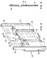
- Figs. 5 and 6 illustrate an example of such an embodiment, wherein a plastic liner 60 for defibrillation circuitry has a circuitous resistive path 61 molded therein, which resistive path 61 defines an energy dissipation resistor in accordance with the present invention.
- the plastic liner 60 comprises two enlongated support arms 62 and 64 for supporting a defibrillation circuit board 66; two cylindrical support members 68 and 70 for receiving and upporting a pair of capacitors 72 and 74; a planar center member 76 for supporting a pair of adhesively attached rectangular batteries (not shown); and a circuitous resistive path 61 molded inside the plastic of the planar center member 76.
- the resitive path 61 defines an energy dissipation resistor which is integrally formed within the plastic liner 60.
- the circuitous resistive path is electrically connected to the circuit board 66 via a pair of electrically conductive contacts 78 and 80 and leads 82 and 84.
- the combination of the liner 60, the circuit board 66, and the two capacitors 72 and 74 typically measures 7,62 cm (3 inches) in heigth, 7,62 cm (3 inches) in width, and 1,9 cm (0,75 inches) in thickness.
- the planar center member 76 has a surface area of between 12,9 and 25,8 cm 2 (2 in 2 and 4 in 2 ), with an overall thickness of approximately 0,0127cm (0,005").
- electro-depositing techniques can also be utilized to deposit the energy dissipation resistor of the present invention directly onto a plastic liner for a defibrillation ciruit.
- the energy dissipation resistor can be incorporation into, or printed onto, an analog or digital hybrid substrate.
- Hybrid substrates typically comprise a rigid ceramic or cofire ceramic material having favorable electrical properties, such as high resistance to dielectric breakdown.
- the resistor can be incorporated into the substrate using any of the foregoing arrangements or methods for incorporating the resistor into a flexible circuit board.
Landscapes
- Health & Medical Sciences (AREA)
- Cardiology (AREA)
- Heart & Thoracic Surgery (AREA)
- Engineering & Computer Science (AREA)
- Biomedical Technology (AREA)
- Nuclear Medicine, Radiotherapy & Molecular Imaging (AREA)
- Radiology & Medical Imaging (AREA)
- Life Sciences & Earth Sciences (AREA)
- Animal Behavior & Ethology (AREA)
- General Health & Medical Sciences (AREA)
- Public Health (AREA)
- Veterinary Medicine (AREA)
- Electrotherapy Devices (AREA)
Claims (25)
- Implantierbarer Herz-Defibrillator mit mindestens einer Einrichtung für die Speicherung elektrischer Energie, welcher Defibrillator einen inneren energetisch dissipativen Widerstand (2) für die Dissipation elektrischer Energie aufweist, die in der genannten mindestens einen Einrichtung für die Speicherung elektrischer Energie gespeichert ist,
dadurch gekennzeichnet, daß
der Widerstand (2) eine geringe Querschnittsdicke, aber eine große Oberfläche besitzt, so daß eine maximale Dissipation von Wärmeenergie erfolgt, und daß der Widerstand (2) umfaßt:eine Schicht (4) von elektrischer Widerstandsfolie, die eine mehrfach gewundene Widerstandsbahn bildet;eine erste (6) und eine zweite (8) Lage Isoliermaterial an den entgegengesetzt gerichteten Seiten der Folie; undmindestens zwei elektrisch leitende Kontaktstücke (14,16), die mindestens zwei elektrisch leitende Wege durch mindestens eine der ersten Lage (6) und der zweiten (8) Lage von elektrisch isolierendem Material bieten, um eine elektrische Verbindung mit der Widerstandsfolie herzustellen. - Implantierbarer Herz-Defibrillator nach Anspruch 1, worin der Widerstand (2) außerdem ein Verbindungsmittel (10) zum isolierenden Verbinden der Widerstandsfolie mit der ersten (6) und der zweiten Lage (8) von elektrisch isolierendem Material aufweist.
- Implantierbarer Herz-Defibrillator nach Anspruch 1, worin der genannte mindestens eine Speicher für elektrische Energie einen Defibrillations-Kondensator (C1, C2) darstellt.
- Implantierbarer Herz-Defibrillator nach Anspruch 3, ferner versehen mit einer Einrichtung (S2) zum wahlweisen Anschließen des Widerstands (2) an den genannten Defibrillations-Kondensator (C1, C2).
- Implantierbarer Herz-Defibrillator nach Anspruch 1, ferner umfassend: eine Schicht (34) elektrisch leitender Stromleiterbahnen (36, 38), angrenzend an die zweite Lage (42) von elektrisch isolierendem Material, wobei mindenstens zwei der Stromleiterbahnen (36, 38) elektrisch verbunden sind mit den genannten mindestens zwei elektrisch leitenden Kontaktstücken (44, 46); und eine dritte Lage (40) elektrisch isolierendes Material,angrenzend an die Schicht (34) von elektrisch leitenden Stromleiterbahnen (36, 38), worin die Schicht (34) von elektrisch leitenden Stromleiterbahnen (36,38) und eine dritte Lage (40) von elektrisch isolierendem Material zumindest einen Teil einer Defibrillator-Leiterplatte (32) bilden.
- Implantierbarer Herz-Defibrillator nach Anspruch 3, ferner umfassend:einen Ladekreis zum Laden des genannten mindestens einen Kondensators (C1, C2);mindestens zwei Elektroden (24, 26), um einem Patienten die in dem genannten mindestens einen Defibrillations-Kondensator (C1, C2) gespeicherte elektrische Energie zuzuführen; undeine Einrichtung (S1), um wahlweise die genannten mindestens zwei Elektroden (24, 26) mit dem genannten mindestens einen Defibrillations-Kondensator (C1, C2) zu verbinden, und (S2), um wahlweise den genannten Energiedissipations-Widerstand (2) mit dem genannten mindestens einen Defibrillations-Kondensator (C1, C2) zu verbinden.
- Implantierbarer Herz-Defibrillator nach Anspruch 6, worin der Energiedissipations-Widerstand (2) außerdem ein Verbindungsmittel (10) aufweist, um die genannte Schicht (4) von Widerstandsfolie zwischen der genannten ersten (6) und zweiten (8) Lage von elektrisch isolierendem Material zu verkleben.
- Implantierbarer Herz-Defibrillator nach Anspruch 7, worin das genannte Verbindungsmaterial (10) aus TEFLON® besteht.
- Implantierbarer Herz-Defibrillator nach Anspruch 6, worin die elektrische Widerstandsfolie aus Kupfernickel besteht.
- Implantierbarer Herz-Defibrillator nach Anspruch 6, worin die genannten mindestens zwei elektrisch leitenden Kontaktstücke (14, 16, 44, 46) mit verzinntem Kupfer plattiert sind.
- Implantierbarer Herz-Defibrillator nach Anspruch 6, worin die genannten mindestens zwei elektrisch leitenden Kontaktstücke (14, 16, 44, 46) mit Silber und Blei plattiert sind.
- Implantierbarer Herz-Defibrillator nach Anspruch 6, ferner elektrisch leitende Leiter (14A, 16A) umfassend, die mit jeweils einem der genannten elektrischen Kontaktstücke (14, 16) elektrisch verbunden sind.
- Implantierbarer Herz-Defibrillator nach Anspruch 1, ferner umfassend:eine Defibrillator-Leiterplatte (32) mit dem genannten inneren, energetisch dissipativen Widerstand (30), welche Leiterplatte (32) außerdem umfaßt:eine Schicht (34) elektrisch leitender Leiterbahnen (36, 38) angrenzend an die genannte zweite Lage (42) von elektrisch isolierendem Material, wobei mindestens zwei der genannten Leiterbahnen (36, 38) elektrisch verbunden sind mit den genannten mindestens zwei elektrisch leitenden Kontaktstücken (44, 46), und eine dritte Lage (40) von elektrisch isolierendem Material angrenzend an die genannte Schicht (34) von elektrisch leitenden Leiterbahnen (36, 38).
- Implantierbarer Herz-Defibrillator nach Anspruch 13, und weiter umfassend Verbindungsmaterial zum Verkleben aneinandergrenzender Lagen der Leiterkarte miteinander.
- Implantierbarer Herz-Defibrillator nach Anspruch 14, worin das genannte Verbindungsmaterial aus TEFLON® besteht.
- Implantierbarer Herz-Defibrillator nach Anspruch 13, worin die elektrische Widerstandsfolie aus Kupfernickel besteht.
- Implantierbarer Herz-Defibrillator nach Anspruch 13, worin die genannten mindestens zwei leitenden Kontaktstücke (44, 46) mit verzinntem Kupfer plattiert sind.
- Leiterplatte nach Anspruch 13, worin die genannten mindestens zwei leitenden Kontaktstücke (44, 46) mit Silber und Blei plattiert sind.
- Implantierbarer Herz-Defibrillator nach Anspruch 1, ferner umfassend:einen Einsatz 60 zur Aufnahme der Komponenten einer implantierbaren Defibrillations-Schaltung, welcher Einsatz (60) umfaßt:den genannten, zur Energiedissipation dienenden Widerstand, der eingeschlossen und definiert ist durch eine mehrfach gewundene Widerstandsbahn (61), die innerhalb' des den Einsatz (60) bildenden Materials verläuft; undmindestens zwei elektrisch leitende Kontaktstücke (78, 80), die mindestens zwei elektrisch leitende Bahnen durch eine Oberfläche des Einsatzes (60) bieten, um die elektrische Verbindung mit dem als bauliche Einheit ausgeführten Energiedissipations-Widerstand herzustellen.
- Implantierbarer Herz-Defibrillator nach Anspruch 19, ferner elektrisch leitende Leiter (82, 84) umfassend, die an jeweils zugeordnete der genannten mindestens zwei elektrisch leitende Kontaktstücke (78, 80) angeschlossen sind.
- Implantierbarer Herz-Defibrillator nach Anspruch 19, worin das genannte Material, aus dem der Einsatz (60) besteht, ein Kunststoffmaterial ist.
- Implantierbarer Herz-Defibrillator nach Anspruch 19, worin die genannten mindestens zwei elektrisch leitenden Kontaktstücke (78, 80) entweder mit Silber und Blei oder mit verzinntem Kupfer plattiert sind.
- Implantierbarer Herz-Defibrillator nach Anspruch 19, worin die genannte mehrfach gewundene Widerstandsbahn (61) eine Widerstandsfolie von 70 % Kupfer - 30 % Nickel darstellt mit einer Länge zwischen 432 und 635 cm (170 und 250 in.), einer Breite zwischen 0,01 und 0,025 cm (0,004 und 0,01 in.) und einer Dicke zwischen 0,0015 und 0,0018 cm (0,0006 und 0,0007 inches), wobei die Länge wahlweise so gewählt wird, daß ein Gesamtwiderstand zwischen 850 Ohm und 1150 Ohm erreicht wird.
- Implantierbarer Herz-Defibrillator nach Anspruch 19, ferner umfassend:ein ebenes Mittelteil (76) zum Aufnehmen von mindestens einer Batterie, wobei die mehrfach gewundene Widerstandsbahn (61) sich innerhalb des Materials befindet, das das ebene Mittelteil (76) bildet;zwei zylindrische Tragelemente (68, 70) zum Aufnehmen und Halten von zwei Kondensatoren (72, 74), wobei die beiden genannten zylindrischen Tragelemente (68, 70) zueinander parallel sind und an den entgegengesetzten Enden des ebenen Mittelteils (76) mit diesem baulich verbunden ausgebildet sind; undzwei parallel zueinander verlaufende längliche Tragarme (62, 64), die zur Aufnahme einer Defibrillations-Leiterplatte (66) so an jeweils eines der genannten zylindrischen Halteteile (68, 70) angeformt sind, daß sie von diesen nach außen verlaufen.
- Implantierbarer Herz-Defibrillator nach Anspruch 24, worin das ebene Mittelteil (76) eine Flächengröße zwischen 12,9 und 25,8 cm2 (2 in2 und 4 in2) und eine Gesamtdicke von ungefähr 0,0127 cm (0,005") hat.
Applications Claiming Priority (2)
| Application Number | Priority Date | Filing Date | Title |
|---|---|---|---|
| US07/878,537 US5312442A (en) | 1992-05-05 | 1992-05-05 | Energy dissipation resistor for implantable defibrillation circuitry |
| US878537 | 1992-05-05 |
Publications (3)
| Publication Number | Publication Date |
|---|---|
| EP0568960A2 EP0568960A2 (de) | 1993-11-10 |
| EP0568960A3 EP0568960A3 (de) | 1995-05-10 |
| EP0568960B1 true EP0568960B1 (de) | 1999-08-04 |
Family
ID=25372227
Family Applications (1)
| Application Number | Title | Priority Date | Filing Date |
|---|---|---|---|
| EP93107173A Expired - Lifetime EP0568960B1 (de) | 1992-05-05 | 1993-05-03 | Implantierbarer Herz-Defibrillator mit energetisch dissipativem Widerstand |
Country Status (10)
| Country | Link |
|---|---|
| US (1) | US5312442A (de) |
| EP (1) | EP0568960B1 (de) |
| JP (1) | JP2774919B2 (de) |
| AT (1) | ATE182802T1 (de) |
| AU (1) | AU648464B2 (de) |
| CA (1) | CA2095562C (de) |
| DE (1) | DE69325847T2 (de) |
| DK (1) | DK0568960T3 (de) |
| ES (1) | ES2137956T3 (de) |
| GR (1) | GR3031594T3 (de) |
Families Citing this family (12)
| Publication number | Priority date | Publication date | Assignee | Title |
|---|---|---|---|---|
| US5645586A (en) * | 1994-07-08 | 1997-07-08 | Ventritex, Inc. | Conforming implantable defibrillator |
| US5749910A (en) * | 1995-06-07 | 1998-05-12 | Angeion Corporation | Shield for implantable cardioverter defibrillator |
| US5716381A (en) * | 1996-08-06 | 1998-02-10 | Pacesetter, Inc. | Electrophysiology diagnostic device including variable capacitance emulation and voltage threshold determination circuits |
| US5876439A (en) * | 1996-12-09 | 1999-03-02 | Micooptix, Llc | Method and appartus for adjusting corneal curvature using a fluid-filled corneal ring |
| US6094597A (en) * | 1999-02-05 | 2000-07-25 | Medtronic, Inc. | Implantable medical device incorporating distributed core, step-up transformer |
| US6185456B1 (en) * | 1999-02-26 | 2001-02-06 | Medical Research Laboratories, Inc. | Defibrillator disarm circuit utilizing thermal feedback |
| US6353760B1 (en) | 1999-04-30 | 2002-03-05 | Cardiac Pacemakers, Inc. | Implantable cardiac stimulating device with optimized demand |
| US6539258B1 (en) | 2000-10-06 | 2003-03-25 | Medtronic Physio-Control Manufacturing Corp. | Energy adjusting circuit for producing an ultra-low energy defibrillation waveform with fixed pulse width and fixed tilt |
| TWI497535B (zh) | 2011-07-28 | 2015-08-21 | Cyntec Co Ltd | 具有軟性材料層之微電阻元件及其製造方法 |
| US8749949B2 (en) * | 2011-10-31 | 2014-06-10 | Lawrence Livermore National Security, Llc | Resistive foil edge grading for accelerator and other high voltage structures |
| DE102018101419A1 (de) * | 2018-01-23 | 2019-07-25 | Biotronik Se & Co. Kg | Elektrischer Widerstand, insbesondere für medizinische Implantate |
| DE102018114801B4 (de) * | 2018-06-20 | 2025-04-17 | Dyconex Ag | Diffusionsbarriere für implantierbare Elektrodenleitungen |
Citations (1)
| Publication number | Priority date | Publication date | Assignee | Title |
|---|---|---|---|---|
| US4316472A (en) * | 1974-04-25 | 1982-02-23 | Mieczyslaw Mirowski | Cardioverting device with stored energy selecting means and discharge initiating means, and related method |
Family Cites Families (15)
| Publication number | Priority date | Publication date | Assignee | Title |
|---|---|---|---|---|
| US2482316A (en) * | 1945-05-26 | 1949-09-20 | Amalgamated Wireless Australas | Lamella resistance unit |
| US2521894A (en) * | 1950-02-08 | 1950-09-12 | Robert J S Brown | Low inductance resistor |
| US3654580A (en) * | 1969-03-14 | 1972-04-04 | Sanders Associates Inc | Resistor structure |
| FR2053539A5 (de) * | 1969-07-08 | 1971-04-16 | Electronique Appliquee | |
| GB1319765A (en) * | 1969-10-15 | 1973-06-06 | Atomic Energy Authority Uk | Resistive elements |
| US3798542A (en) * | 1972-07-05 | 1974-03-19 | R Dempsey | Energy measuring device for pulse type defibrillators |
| DE2450551C2 (de) * | 1974-10-24 | 1977-01-13 | Heraeus Gmbh W C | Elektrischer messwiderstand fuer ein widerstandsthermometer und verfahren zu seiner herstellung |
| US4164946A (en) * | 1977-05-27 | 1979-08-21 | Mieczyslaw Mirowski | Fault detection circuit for permanently implanted cardioverter |
| US4297670A (en) * | 1977-06-03 | 1981-10-27 | Angstrohm Precision, Inc. | Metal foil resistor |
| US4254775A (en) * | 1979-07-02 | 1981-03-10 | Mieczyslaw Mirowski | Implantable defibrillator and package therefor |
| DE3201434A1 (de) * | 1982-01-19 | 1983-09-08 | Siemens AG, 1000 Berlin und 8000 München | Elektrisches bauelement in chip-bauweise |
| DE3229134A1 (de) * | 1982-08-04 | 1984-02-09 | GS Elektromed. Geräte Günter Stemple, 8912 Kaufering | Elektrische schaltung zur erzeugung von energieimpulsen an zwei schockelektroden eines defibrillators |
| US4488555A (en) * | 1982-12-13 | 1984-12-18 | Mieczyslaw Mirowski | Battery condition warning system for medical implant |
| FR2646019B1 (fr) * | 1989-04-14 | 1991-07-19 | Sgs Thomson Microelectronics | Resistance spirale haute tension |
| US5163427A (en) * | 1990-11-14 | 1992-11-17 | Medtronic, Inc. | Apparatus for delivering single and multiple cardioversion and defibrillation pulses |
-
1992
- 1992-05-05 US US07/878,537 patent/US5312442A/en not_active Expired - Lifetime
-
1993
- 1993-05-03 AT AT93107173T patent/ATE182802T1/de not_active IP Right Cessation
- 1993-05-03 DK DK93107173T patent/DK0568960T3/da active
- 1993-05-03 EP EP93107173A patent/EP0568960B1/de not_active Expired - Lifetime
- 1993-05-03 ES ES93107173T patent/ES2137956T3/es not_active Expired - Lifetime
- 1993-05-03 DE DE69325847T patent/DE69325847T2/de not_active Expired - Lifetime
- 1993-05-05 AU AU38386/93A patent/AU648464B2/en not_active Ceased
- 1993-05-05 CA CA002095562A patent/CA2095562C/en not_active Expired - Fee Related
- 1993-05-06 JP JP5105588A patent/JP2774919B2/ja not_active Expired - Fee Related
-
1999
- 1999-10-21 GR GR990402688T patent/GR3031594T3/el unknown
Patent Citations (2)
| Publication number | Priority date | Publication date | Assignee | Title |
|---|---|---|---|---|
| US4316472A (en) * | 1974-04-25 | 1982-02-23 | Mieczyslaw Mirowski | Cardioverting device with stored energy selecting means and discharge initiating means, and related method |
| US4316472C1 (en) * | 1974-04-25 | 2001-08-14 | Mieczyslaw Mirowski | Cardioverting device with stored energy selecting means and discharge initiating means and related method |
Also Published As
| Publication number | Publication date |
|---|---|
| ATE182802T1 (de) | 1999-08-15 |
| EP0568960A2 (de) | 1993-11-10 |
| DE69325847D1 (de) | 1999-09-09 |
| DE69325847T2 (de) | 2000-01-13 |
| EP0568960A3 (de) | 1995-05-10 |
| JP2774919B2 (ja) | 1998-07-09 |
| JPH07265443A (ja) | 1995-10-17 |
| CA2095562C (en) | 1997-03-25 |
| AU648464B2 (en) | 1994-04-21 |
| AU3838693A (en) | 1993-11-11 |
| DK0568960T3 (da) | 1999-12-06 |
| CA2095562A1 (en) | 1993-11-06 |
| ES2137956T3 (es) | 2000-01-01 |
| US5312442A (en) | 1994-05-17 |
| GR3031594T3 (en) | 2000-01-31 |
Similar Documents
| Publication | Publication Date | Title |
|---|---|---|
| EP0568960B1 (de) | Implantierbarer Herz-Defibrillator mit energetisch dissipativem Widerstand | |
| US7554424B2 (en) | Electronic component and method of making | |
| US5637418A (en) | Package for a flat electrochemical device | |
| US5978204A (en) | Capacitor with dual element electrode plates | |
| US5367431A (en) | Thin power supply unit | |
| US6611421B2 (en) | Non-polarized tantalum capacitor and capacitor array | |
| US4748537A (en) | Decoupling capacitor and method of formation thereof | |
| JPH11162708A (ja) | 多層導電性ポリマ正温度係数デバイス | |
| WO1994019813A1 (en) | Metallized capacitor having increased dielectric breakdown voltage and method for making the same | |
| WO1997020331A1 (en) | Capacitor with dual element electrode plates | |
| JP2003524878A (ja) | 改善した導電性ポリマーデバイス及びその製造方法 | |
| WO2001039214A2 (en) | Improved conductive polymer device and method of manufacturing same | |
| US4599486A (en) | High capacitance bus bar including multilayer ceramic capacitors | |
| US5051542A (en) | Low impedance bus bar | |
| EP1110312B1 (de) | Elektronisches bauteil | |
| JPH06275248A (ja) | 積層型電池の基板への実装構造 | |
| JP2004095816A (ja) | チップ形コンデンサ | |
| JP3666668B2 (ja) | 固体電解コンデンサとコイルとの複合素子の構造 | |
| EP0200670A2 (de) | Entkopplungskondensator und Verfahren zu seiner Herstellung | |
| JPS59188113A (ja) | 電力用コンデンサ | |
| GB2115213A (en) | Laminated bus bar with dielectric inserts | |
| JPH1097945A (ja) | 箔状コンデンサ | |
| JPS6224685A (ja) | コンデンサ組込み配線基板 | |
| JP2000307207A (ja) | プリント配線板の接続部 | |
| JPH08276688A (ja) | 回路チップ担持装置及びその製造方法 |
Legal Events
| Date | Code | Title | Description |
|---|---|---|---|
| PUAI | Public reference made under article 153(3) epc to a published international application that has entered the european phase |
Free format text: ORIGINAL CODE: 0009012 |
|
| AK | Designated contracting states |
Kind code of ref document: A2 Designated state(s): AT BE CH DE DK ES FR GB GR IE IT LI LU MC NL PT SE |
|
| PUAL | Search report despatched |
Free format text: ORIGINAL CODE: 0009013 |
|
| AK | Designated contracting states |
Kind code of ref document: A3 Designated state(s): AT BE CH DE DK ES FR GB GR IE IT LI LU MC NL PT SE |
|
| 17P | Request for examination filed |
Effective date: 19950420 |
|
| 17Q | First examination report despatched |
Effective date: 19980402 |
|
| GRAG | Despatch of communication of intention to grant |
Free format text: ORIGINAL CODE: EPIDOS AGRA |
|
| GRAG | Despatch of communication of intention to grant |
Free format text: ORIGINAL CODE: EPIDOS AGRA |
|
| GRAH | Despatch of communication of intention to grant a patent |
Free format text: ORIGINAL CODE: EPIDOS IGRA |
|
| GRAH | Despatch of communication of intention to grant a patent |
Free format text: ORIGINAL CODE: EPIDOS IGRA |
|
| GRAA | (expected) grant |
Free format text: ORIGINAL CODE: 0009210 |
|
| AK | Designated contracting states |
Kind code of ref document: B1 Designated state(s): AT BE CH DE DK ES FR GB GR IE IT LI LU MC NL PT SE |
|
| REF | Corresponds to: |
Ref document number: 182802 Country of ref document: AT Date of ref document: 19990815 Kind code of ref document: T |
|
| REG | Reference to a national code |
Ref country code: CH Ref legal event code: EP |
|
| REF | Corresponds to: |
Ref document number: 69325847 Country of ref document: DE Date of ref document: 19990909 |
|
| REG | Reference to a national code |
Ref country code: IE Ref legal event code: FG4D |
|
| ITF | It: translation for a ep patent filed | ||
| ET | Fr: translation filed | ||
| REG | Reference to a national code |
Ref country code: CH Ref legal event code: NV Representative=s name: PATENTANWAELTE SCHAAD, BALASS, MENZL & PARTNER AG |
|
| REG | Reference to a national code |
Ref country code: DK Ref legal event code: T3 |
|
| REG | Reference to a national code |
Ref country code: PT Ref legal event code: SC4A Free format text: AVAILABILITY OF NATIONAL TRANSLATION Effective date: 19991011 |
|
| REG | Reference to a national code |
Ref country code: ES Ref legal event code: FG2A Ref document number: 2137956 Country of ref document: ES Kind code of ref document: T3 |
|
| PG25 | Lapsed in a contracting state [announced via postgrant information from national office to epo] |
Ref country code: LU Free format text: LAPSE BECAUSE OF NON-PAYMENT OF DUE FEES Effective date: 20000503 |
|
| PLBE | No opposition filed within time limit |
Free format text: ORIGINAL CODE: 0009261 |
|
| 26N | No opposition filed | ||
| PG25 | Lapsed in a contracting state [announced via postgrant information from national office to epo] |
Ref country code: MC Free format text: LAPSE BECAUSE OF NON-PAYMENT OF DUE FEES Effective date: 20001130 |
|
| REG | Reference to a national code |
Ref country code: GB Ref legal event code: IF02 |
|
| PGFP | Annual fee paid to national office [announced via postgrant information from national office to epo] |
Ref country code: PT Payment date: 20060502 Year of fee payment: 14 Ref country code: IE Payment date: 20060502 Year of fee payment: 14 Ref country code: GR Payment date: 20060502 Year of fee payment: 14 |
|
| PGFP | Annual fee paid to national office [announced via postgrant information from national office to epo] |
Ref country code: GB Payment date: 20060503 Year of fee payment: 14 |
|
| PGFP | Annual fee paid to national office [announced via postgrant information from national office to epo] |
Ref country code: DK Payment date: 20060509 Year of fee payment: 14 |
|
| PGFP | Annual fee paid to national office [announced via postgrant information from national office to epo] |
Ref country code: ES Payment date: 20060511 Year of fee payment: 14 |
|
| PGFP | Annual fee paid to national office [announced via postgrant information from national office to epo] |
Ref country code: NL Payment date: 20060515 Year of fee payment: 14 |
|
| PGFP | Annual fee paid to national office [announced via postgrant information from national office to epo] |
Ref country code: SE Payment date: 20060517 Year of fee payment: 14 |
|
| PGFP | Annual fee paid to national office [announced via postgrant information from national office to epo] |
Ref country code: CH Payment date: 20060519 Year of fee payment: 14 |
|
| PGFP | Annual fee paid to national office [announced via postgrant information from national office to epo] |
Ref country code: AT Payment date: 20060523 Year of fee payment: 14 |
|
| PGFP | Annual fee paid to national office [announced via postgrant information from national office to epo] |
Ref country code: FR Payment date: 20060529 Year of fee payment: 14 |
|
| PGFP | Annual fee paid to national office [announced via postgrant information from national office to epo] |
Ref country code: BE Payment date: 20060530 Year of fee payment: 14 |
|
| REG | Reference to a national code |
Ref country code: PT Ref legal event code: MM4A Free format text: LAPSE DUE TO NON-PAYMENT OF FEES Effective date: 20071105 |
|
| BERE | Be: lapsed |
Owner name: *CARDIAC PACEMAKERS INC. Effective date: 20070531 |
|
| EUG | Se: european patent has lapsed | ||
| REG | Reference to a national code |
Ref country code: CH Ref legal event code: PL |
|
| REG | Reference to a national code |
Ref country code: DK Ref legal event code: EBP |
|
| GBPC | Gb: european patent ceased through non-payment of renewal fee |
Effective date: 20070503 |
|
| PG25 | Lapsed in a contracting state [announced via postgrant information from national office to epo] |
Ref country code: PT Free format text: LAPSE BECAUSE OF NON-PAYMENT OF DUE FEES Effective date: 20071105 Ref country code: NL Free format text: LAPSE BECAUSE OF NON-PAYMENT OF DUE FEES Effective date: 20071201 |
|
| NLV4 | Nl: lapsed or anulled due to non-payment of the annual fee |
Effective date: 20071201 |
|
| REG | Reference to a national code |
Ref country code: IE Ref legal event code: MM4A |
|
| PG25 | Lapsed in a contracting state [announced via postgrant information from national office to epo] |
Ref country code: AT Free format text: LAPSE BECAUSE OF NON-PAYMENT OF DUE FEES Effective date: 20070503 Ref country code: LI Free format text: LAPSE BECAUSE OF NON-PAYMENT OF DUE FEES Effective date: 20070531 Ref country code: CH Free format text: LAPSE BECAUSE OF NON-PAYMENT OF DUE FEES Effective date: 20070531 |
|
| REG | Reference to a national code |
Ref country code: FR Ref legal event code: ST Effective date: 20080131 |
|
| PG25 | Lapsed in a contracting state [announced via postgrant information from national office to epo] |
Ref country code: BE Free format text: LAPSE BECAUSE OF NON-PAYMENT OF DUE FEES Effective date: 20070531 |
|
| PG25 | Lapsed in a contracting state [announced via postgrant information from national office to epo] |
Ref country code: DK Free format text: LAPSE BECAUSE OF NON-PAYMENT OF DUE FEES Effective date: 20070531 |
|
| PG25 | Lapsed in a contracting state [announced via postgrant information from national office to epo] |
Ref country code: IE Free format text: LAPSE BECAUSE OF NON-PAYMENT OF DUE FEES Effective date: 20070503 Ref country code: GB Free format text: LAPSE BECAUSE OF NON-PAYMENT OF DUE FEES Effective date: 20070503 |
|
| PG25 | Lapsed in a contracting state [announced via postgrant information from national office to epo] |
Ref country code: SE Free format text: LAPSE BECAUSE OF NON-PAYMENT OF DUE FEES Effective date: 20070504 |
|
| PG25 | Lapsed in a contracting state [announced via postgrant information from national office to epo] |
Ref country code: FR Free format text: LAPSE BECAUSE OF NON-PAYMENT OF DUE FEES Effective date: 20070531 |
|
| REG | Reference to a national code |
Ref country code: ES Ref legal event code: FD2A Effective date: 20070504 |
|
| PG25 | Lapsed in a contracting state [announced via postgrant information from national office to epo] |
Ref country code: GR Free format text: LAPSE BECAUSE OF NON-PAYMENT OF DUE FEES Effective date: 20071204 Ref country code: ES Free format text: LAPSE BECAUSE OF NON-PAYMENT OF DUE FEES Effective date: 20070504 |
|
| PG25 | Lapsed in a contracting state [announced via postgrant information from national office to epo] |
Ref country code: IT Free format text: LAPSE BECAUSE OF NON-PAYMENT OF DUE FEES Effective date: 20090503 |
|
| PGFP | Annual fee paid to national office [announced via postgrant information from national office to epo] |
Ref country code: DE Payment date: 20110427 Year of fee payment: 19 |
|
| PGFP | Annual fee paid to national office [announced via postgrant information from national office to epo] |
Ref country code: IT Payment date: 20110516 Year of fee payment: 19 |
|
| PG25 | Lapsed in a contracting state [announced via postgrant information from national office to epo] |
Ref country code: IT Free format text: LAPSE BECAUSE OF NON-PAYMENT OF DUE FEES Effective date: 20120503 |
|
| REG | Reference to a national code |
Ref country code: DE Ref legal event code: R119 Ref document number: 69325847 Country of ref document: DE Effective date: 20121201 |
|
| PG25 | Lapsed in a contracting state [announced via postgrant information from national office to epo] |
Ref country code: DE Free format text: LAPSE BECAUSE OF NON-PAYMENT OF DUE FEES Effective date: 20121201 |