EP0568911B1 - Anordnung zur Übertragung von Farbfernsehsignalen mit einem Leuchtdichtesignal und wenigstens einem diesem zugeordneten Farbsignal - Google Patents
Anordnung zur Übertragung von Farbfernsehsignalen mit einem Leuchtdichtesignal und wenigstens einem diesem zugeordneten Farbsignal Download PDFInfo
- Publication number
- EP0568911B1 EP0568911B1 EP93106860A EP93106860A EP0568911B1 EP 0568911 B1 EP0568911 B1 EP 0568911B1 EP 93106860 A EP93106860 A EP 93106860A EP 93106860 A EP93106860 A EP 93106860A EP 0568911 B1 EP0568911 B1 EP 0568911B1
- Authority
- EP
- European Patent Office
- Prior art keywords
- signal
- colour
- edge
- luminance
- color
- Prior art date
- Legal status (The legal status is an assumption and is not a legal conclusion. Google has not performed a legal analysis and makes no representation as to the accuracy of the status listed.)
- Expired - Lifetime
Links
Images

Classifications
-
- H—ELECTRICITY
- H04—ELECTRIC COMMUNICATION TECHNIQUE
- H04N—PICTORIAL COMMUNICATION, e.g. TELEVISION
- H04N5/00—Details of television systems
- H04N5/14—Picture signal circuitry for video frequency region
- H04N5/142—Edging; Contouring
-
- H—ELECTRICITY
- H04—ELECTRIC COMMUNICATION TECHNIQUE
- H04N—PICTORIAL COMMUNICATION, e.g. TELEVISION
- H04N9/00—Details of colour television systems
- H04N9/64—Circuits for processing colour signals
- H04N9/646—Circuits for processing colour signals for image enhancement, e.g. vertical detail restoration, cross-colour elimination, contour correction, chrominance trapping filters
Definitions
- the invention relates to an arrangement for the transmission of color television signals which contain a luminance signal and at least one color signal associated therewith in accordance with the text specified in the preamble of claim 1.
- EP-A-0 302 500 discloses such an arrangement.
- the color information of a color television image is generally transmitted separately from the luminance information, in particular in order to maintain compatibility with the black and white transmission of such a television image.
- the transmission of the color signals for such color information has a significantly smaller frequency bandwidth available than the transmission of the associated luminance signals.
- the color signal changes the transmission mode more frequently than the associated luminance signal.
- the color signal within a transmission of a color television picture is more frequently exposed to interference points within the transmission path than the luminance signal.
- a circuit for eliminating the above-described false colors in the color fringe of a vertical color edge which differentiates in the color difference transmission channels of a color television edge detectors contains an edge detector arrangement.
- Each edge detector generates at its output a detector signal which is dependent on the type of the detected signal edge and which differentiates again in a subsequent pulse shaper of the arrangement and is then fed to a circuit with a set switching threshold.
- the switching signals of the edge detector arrangement thus generated control an analog switch in the transmission line, to the output side of which a storage capacitor is connected.
- the analog switch is interrupted during the duration of the switching signal of the edge detector arrangement, so that during the interrupted state of the analog switch, the storage capacitor determines the level of the transmission channel on the output side and keeps the transmission signal at the level last present before the analog switch was opened.
- the analog switch is closed again, i.e. after the end of the signal edge, the signal on the output transmission line changes with the relatively short charging time of the storage capacitor to the level of the signal state after the signal edge, so that the steepness of the corrected signal edge only depends on the short charging time of the Storage capacitor is dependent.
- the annoying false color fringes on vertical color edges have not been eliminated and a disturbed, fluffy color image is still displayed on the television screen.
- a transmission arrangement for the transmission of color television signals for the reproduction of a color television picture on a screen in which a delay line is arranged both in the transmission path of the luminance signal and in the transmission path of the associated color signal of the color television signals is.
- the transmission path of the color signals also contains a signal switch, the signal output of which is connected to the output of the delay line in one switch position of the signal switch and to the input of the delay line in the other switch position of the signal switch.
- the signal switch is controlled both by a color edge detector which detects the color signal and by a luminance jump detector which detects the luminance signal.
- the CVBS output signal is formed from the delayed color signal and the delayed luminance signal.
- the signal output of the signal switch is switched during the transmission of the delayed color jump to the input of the delay circuit in the transmission path of the color signal, on which the new color signal is already behind the color jump.
- the false-colored interference stripe on a vertical color edge is largely eliminated by the measures just described.
- the color edge still has an annoying jitter, which makes the color edge disturbing.
- This disturbance is particularly severe in the case of fairly noisy color television signals or when the color television signal changes from one color type via a relatively flat signal edge to another color type and the slope of the signal edge of the color edge shown fluctuates from line to line.
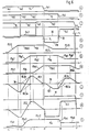
- the shape and amplitude of the detection signals which are generated in the processing circuits of the edge detectors depend on the nature of the detected signal edges, so that they trigger very different detection times on a switching edge with respect to the start of the switching edge. This leads to a flickering color edge that is perceived as annoying. This process is shown schematically in diagrams (a) to (d) of FIG. 1.
- Diagram (a) schematically shows the signal edges 1.1, 1.2 and 1.3 of three transmitted color signals 2.1, 2.2 and 2.3, each of which within a flank duration Tf from a level P1.1, P1.2 or P1.3 representing a color F1 a level representing a color F2 P2.1, P2.2 or P2.3 increase.
- Diagram (b) schematically shows the three associated bell-shaped detection signals 3.1, 3.2 and 3.3 of an edge detector (not described in more detail).
- the reference level Ps is drawn in the diagram (b), at which the part of a detector signal exceeding this reference level generates a switching signal shown in the diagram (c) at the output of a threshold switch of this detector arrangement.
- the part 4.3 of the detector signal 3.3 that exceeds the reference level Ps generates the switching signal 6.3. Since the three detection signals 3.1, 3.2 and 3.3 themselves have very different amplitudes and slope slopes, they pass through the reference level Ps of the detector arrangement on very different sides t1, t2 or t3, even though they start at the same starting time to. However, these latter different times determine switching edges 5.1, 5.2 and 5.3 for the detection time of the detected signal edges.
- diagram (d) there are schematically five video lines z1 to z5 of a video image with a vertical color edge K between the two areas with the color F1 to the left of the color edge and F2 to the right of the color edge K. The one caused by the different switching edges 5.1, 5.2 and 5.3 Jitter that changes continuously can be clearly seen in diagram (d).
- the invention has for its object to provide an arrangement specified in the preamble for the transmission of color television signals which contain a luminance signal and at least one color signal associated therewith in such a way that, in particular on the vertical color edges, there are no disturbing, incorrectly colored fringes and no disturbing color edge jitter.
- two identical, offset, but still overlapping difference signals are generated on the edge of the delayed signal to be detected.
- an edge difference signal is produced which oscillates definedly around a zero line and one in the area of overlap of the two individual signals in the middle of the edge difference signal Contains zero crossing at the steepest point of the signal. The position of the zero crossing is largely independent of the shape and the amplitude of the individual signals generated during the detection.
- the superimposed delayed and undelayed color signals do not result in a flattened image, but on the contrary, a lower-noise image with much less disturbed color areas.
- the image disturbances due to lower switching disturbances of the signal switch are lower, since the central position of the signal switch in normal operation means that the distance to the two signal states before and after the transition edge is at least smaller when switching off and in the idle state outside the color edge than in the prior art .
- the changeover device of the signal changeover switch is an electronic cross-fading potentiometer, which can be controlled directly or via an actuating signal amplifier by the edge difference signal generated by the edge detector arrangement.
- the compensation process for suppressing the faulty color fringe is easily adaptable to the type of transition on the signal flank from one signal state to the other signal state, so that little changes are made to the transmission process in the event of minor changes in state and thus there are also fewer disturbances due to this intervention in the transmission process are to be expected.
- the transmission of the color signal to detectable color signal edges is additionally detected. This ensures that the annoying color fringes on color edges that are not characterized by a jump in luminance and annoying jitter on these color edges are significantly reduced so that they no longer catch the eye.
- Another advantageous measure to include the result of a color edge detection in the removal of a disturbing color fringe on this color edge is to superimpose a certain proportion of the output signal of the color edge detection on the output signal of the detection of the associated luminance edge. As a result, the interference suppression of the color edge is adapted to the disturbance variables causing these disturbances.
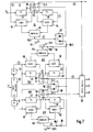
- Figure 2 shows a block diagram of an embodiment of an arrangement for transmitting color television signals for reproducing a color television image on a screen, not shown.
- the transmission arrangement is arranged, for example, in front of the frequency demodulator 7 in the playback part of a video recorder (not shown in more detail).
- the transmission arrangement contains a transmission path 8 with a delay line 9 for the transmission of the frequency-modulated luminance signal Ya of the color television signal and a transmission path 10 with a delay line 11, a signal switch 12 and an additional delay line 13 for transmission of the color signal FSf of the color television signal.
- the transmission path 10 for the color signal is connected to the output 15.2 of a bandpass 15, which is tuned to the color carrier frequency f (FT).
- the signal switch 12 contains three switch positions 12a, 12b and 12c, of which the middle switch position 12b is connected to the two outer switch positions 12a and 12c via two identical ohmic resistors 16.
- the first signal input 12.1 of the signal switch 12 connected to the outer switch position 12a is connected to the output 11.2 of the delay line 11 in the transmission path 10 of the color signal
- the second signal input 12.2 connected to the second outer switch position 12c of the signal switch is connected to the input 11.1 of this delay line 11 .
- the signal switch 12 contains a switch control 20, which generates an actuating signal 21 for setting the signal switch to the switch position 12a, 12b or 12c.
- An edge detector arrangement 24 as well as two threshold value switches 25a and 25c and a zero crossing detector 26 are connected between the input 9.1 of the delay line 9 in the transmission path 8 and the control inputs 20a to 20c of the switch control 20.
- the edge detector arrangement 24 essentially consists of the series connection of two delay lines 27 and 28, of which the input 27.1 of the first delay line 27 of the series circuit is connected to the input 9.1 of the delay line 9 in the transmission path 8, and a signal processing circuit 29 with two signal difference transmitters 30dl and 30d2 and a subtractor 31.
- the differential inputs of the first signal difference transmitter 30dl form the first Differential input pair 29.11 and 29.12 of the signal processing circuit 29 and the differential inputs of the second signal difference generator 30d2 form the second differential input pair 29.21 and 29.22 of the signal processing circuit.
- These differential inputs are connected via signal converters 32 to the inputs 27.1 and 28.1 and the outputs 27.2 and 28.2 of the two delay lines 27 and 28 of the edge detector arrangement 24 connected in series, in such a way that the first signal difference generator 30dl along the first delay line 27 and the second signal difference generator 30d2 along the second delay line 28 is arranged.
- the signal converters 32 serve to convert the signals Ya, Yb, Yc present at the inputs and outputs of the delay lines 27 and 28 into equivalent output signals, which are designed such that the signal difference transmitters 30d1 and 30d2 each one of the signal values of the equivalent output signals Form the difference of the signals Ya, Yb, or, Yb, Yc corresponding difference value and each generate a difference signal 32dl and 32d2 corresponding to this difference value at their signal output 30.3.
- the delay time Tvll of the delay line 11 in the transmission path 10 of the color signal FSf is dimensioned in the exemplary embodiment shown such that it is exactly an odd integer multiple of half the oscillation time T (FT) of the color carrier minus the running time of the inverter 14 connected in the illustrated exemplary embodiment of this delay line 11 and only is slightly longer than the largest expected edge duration T (SF) of the signal edges of the color signal causing the disturbing color fringe.
- Edge duration is understood to mean the duration of the time range of a signal edge that causes the visually visible, disturbing color fringe.
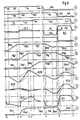
- Diagram (a) schematically shows a section of the undelayed frequency-modulated light density signal Ya at the input 9.1 of the delay line 9 in the transmission path 8 of this signal and at the input 27.1 of the first delay line 27 of the edge detector arrangement 24, the diagram (b) shows the luminance signal simply delayed by this delay line Yb at the output 27.2 of this delay line and the diagram (c) the luminance signal Yc delayed again by the second delay line 28 of the edge detector arrangement 24.
- the Undelayed luminance signal Ya contains a luminance jump SYa3 at time t0, at which the luminance signal jumps in a steeply rising signal edge Ya3 from a first signal state Ya1 representing a first luminance value to a second signal state Ya2 representing a second luminance value, and a second smaller luminance jump SYa4 at time t5 , at which the luminance signal Ya changes over a second signal edge Ya4 from the second signal state Ya2 into a third signal state Ya5 representing a third luminance value. Accordingly, the simply delayed luminance signal Yb at points t1 and t7 and the delayed luminance signal Yc at times t4 and t9 are obtained.
- the first signal difference generator 30dl forms a difference signal 32d1 at its output 30.3 from the difference between the undelayed luminance signal Ya from the output of the first signal converter 32 and the delayed luminance signal Yb from the output of the second signal converter 32 between the luminance jump SYa3 and the luminance jump SYb3 of the simply delayed luminance signal Yb. that is the image of the signal difference between the signal Ya at the input 27.1 and the simply delayed luminance signal Yb at the output 27.2 of the first delay line 27 of the edge detector arrangement 24.
- the second signal difference generator 28 forms a second difference signal 32d2 at its output 30.3 between the luminance jump SYb3 of the simply delayed luminance signal Yb from the output of the second signal converter 32 and the luminance jump SYc3 of the further delayed luminance signal Yc at the output of the third signal converter 32 of the edge detector arrangement 24.
- the two through the signal difference transmitter 30dl and 30d2 Signal difference signals 32d1 and 32d2 generated are shown in the diagrams (d1) and (d2) of FIG.
- the signal difference transmitters 30d1 and 30d2 are designed such that they only output the signal difference signals they form at their signal output 30.3 in one polarity direction, in the exemplary embodiment shown only in the electrically positive polarity direction. Due to the way in which the two signal difference signals 32d1 and 32d2 are generated, these two signals overlap in time in the region 33 of the edge rise time T (FSL3).
- the subtractor 31 subtracts the two identical signals, so that at its signal output, which represents the detection output 24.3 of the edge detection arrangement 24 shown in FIG. 2, an edge difference signal 34.1 and in the area of the second luminance jump SYb4 of the delayed luminance signal Yb, a second edge difference signal 34.2 is generated both are shown in diagram (d) of FIG. 3.
- Both edge difference signals 34.1 and 34.2 oscillate around a zero line 35 with a first oscillation 34a which is negatively directed in the illustrated embodiment and with a subsequent second oscillation 34b which is positively directed in the illustrated embodiment and pass through the zero line in the middle t2 of the overlap region 33 of the two signal difference signals 32d1 and 32d2 with a zero crossing 36.
- This zero crossing is on the one hand at the steepest point of the edge difference signal 34.1 and on the other hand, temporally in the middle of the signal edge of the luminance jump SYb3 of the simply delayed luminance signal Yb and thus defines the detection time t2 of the luminance jump SYb3 of the delayed luminance signal at the output 27.2 of the first delay line 27 of the edge detection arrangement 24.
- a threshold switch 25a and 25c is connected to the signal output 30.3 of the signal difference transmitters 30dl and 30d2, the switching level Ps of which is shown in the diagrams (dl) and (d2) in FIG. 3 by a dashed line 37. If the level of the signal difference signals 32dl and 32d2 exceeds the switching level Ps of the threshold switches represented by line 37, they generate a switching signal 38d4 and 38d5 at their output 25.1 during the time of exceeding, which is shown in diagrams (d4) and (d5) of FIG. 3 is shown schematically.
- the zero crossing detector 26 at the output of the subtractor 31 generates a switching edge 39.1 of a switching signal 39 in the zero crossing 36 of the edge difference signal 34.1 supplied to it, which is shown schematically together with the switching edge 39.1 in diagram (d3) of FIG. 3. From these three switching signals 38d4, 38d5 and 39, the switch control 20 of the signal switch 12 generates an actuating signal 21, which is shown in the diagram (d6) of FIG.
- a first actuating level P1 and during of the switching signal 38d5 of the second signal difference generator 30d2 has a second actuating level P2 and jumps from the first actuating level P1 to the second actuating level P2 on the switching edge 39.1 of the switching signal 39 of the zero crossing detector 26 and outside of these two switching signals 38d4 and 38d5 has the setting level 0, at which the signal switch is set to the middle switching position 12b.
- the first control level P1 places the signal switch 12 in the first outer switch position 12a, in which the output 12.3 of the signal switch is connected to the output of the delay line 11 of the transmission path 10 for the color signal.
- the second control level P2 places the signal switch 12 in the second switch position 12c, in which the output 12.3 of the signal switch is connected to the input of this delay line 11.
- the luminance jump SYa4 between the signal states Ya2 and Ya5 of the undelayed luminance signal Ya and the delayed luminance signals Yb and Yc is so small that the level of the signal difference signals 32d1.1 and 32d2.1 generated therefrom in the edge detector arrangement 24 corresponds to the switching level Ps of the threshold switches 25a and 25c do not reach and therefore no switching signals are generated at the output of the threshold switches 25a and 25c.
- the edge difference signal 34.2 generated at the output of the subtractor 31 from the signal difference signals 32d1.1 and 32d2.1 does not come into effect in the switch control 20 of the signal switch 12.
- FIG 3 shows a section of the undelayed color signal FSf associated with the undelayed luminance signal Ya, which is present at the second signal input 12.2 of the signal switch 12, while in diagram (g) that which is delayed by the delay line 11 and at the first signal input 12.1 of the signal switch 12 applied color signal FSg is shown in sections.
- the undelayed Color signal FSf has a first signal edge FSf3, in which the color signal changes in an edge rise time T (SF3) from a signal state FSf1 representing a first color type F1 to a signal state FSf2 representing a second color type F2, and that of the first signal edge Ya3 of the in the diagram (a ) is assigned to the luminance signal Ya shown, and a second signal edge FSf4, on which the color signal FSf changes from the signal state FSf2 to a signal state FSf5 representing the color type F3 and which belongs to the signal edge Ya4 of the luminance signal Ya at the point t6.
- T edge rise time
- the curve of the delayed color signal FSg shown in diagram (g), which is offset by the delay time Tv11 from the undelayed color signal FSf, is designed accordingly.
- the rise time T (SF3) of the signal edge FSf3 is significantly greater than the rise time T (SFL3) of the associated signal edge Ya3 of the undelayed luminance signal Ya.
- the signal edge Ya3 of the undelayed luminance signal Ya is timed with respect to the associated signal edge FSf3 of the undelayed color signal FSf so that the center of the signal edge of the luminance signal is temporally on the center of the associated signal edge of the undelayed color signal.
- the delay time Tv13 of the delay line 13 at the output 15.2 of the bandpass 15 is dimensioned such that the signal edge FSf3 of the undelayed color signal FSf is delayed to the extent that the end of the largest expected rise time T (SF3) immediately before the zero crossing 36 at the time t2 of the edge difference signal 34.1 generated by the edge detection arrangement 24.
- the delay time Tv27 of the first delay line 27 of the edge detection arrangement 24 is greater than the expected greatest rise time T (SF3) of a color edge of the color signal FSf, so that the oscillation 34a lying before the zero crossing 36 is always wider in time than the disturbing color fringe.
- Diagram (s) schematically shows the curve of the transmitted color signal FSn at the signal output 12.3 of the signal switch 12.
- the signal output is the fact that the signal switch is set to its first outer switching position 12a by the switching signal 21 before the start of the signal edge FSf3 of the instantaneous color signal FSf in its first outer switching position 12a 12.3 of the signal switch 12 is connected to the output of the delay line 11 in the transmission path of the color signal and transmits the first signal state FSg1 of the delayed color signal FSg representing the first color type F1 until the time t2 of the zero crossing 36 of the edge difference signal 34.1 at the output 24.3 of the edge detection arrangement 24 of the control level of the control signal 21 of the switch control 20 changes from the level value P1 to the second level value P2 and thus switches the signal switch 12 into the second outer switching position 12c.
- the state of the color signal FSn transmitted at the signal output 12.3 of the signal switch changes from the first signal state FSn1 representing the first color type F1 to the second signal state FSn2 representing the second color type F2 with a very steep signal edge FSn3 with the switching speed of the signal switch 12.
- the signal switch 12 is returned to its middle switching position 12b, in which it remains until a next control signal.
- the color signal FSn at the signal output of the signal switch occurs in a weakened form both in the range of second signal edge FSn4 of the undelayed color signal FSf and also in the time domain of the second signal edge FSg4 of the delayed color signal FSg a signal edge.
- the color changes at these two color edges FSn4 and FSn6 are generally so small that they are not noticeable.
- the disturbing signal edge FSf3 of the color signal which generates a color fringe is, however, distributed by switching the transmission at the signal switch 12 such that it forms a sharp color edge without color fringe on the reproduced color image.
- the delay time Tv9 of the delay line 9 in the transmission path 8 of the luminance signal Yn is dimensioned such that the associated luminance edge Yn3 is located temporally at the location of the distributed color edge FSn3, as is shown schematically in diagram (n1) in FIG.
- the switchover of the signal switch 12 from the first outer switch position 12a to the second outer switch position 12c and thus the color jump of the color signal at the signal output 12.3 of the signal switch 12 from the signal state FSnl to the signal state FSn2 always takes place at the time t2 of the zero crossing 36 of associated edge difference signals 34.1 at the output 24.3 of the edge detector arrangement 24.
- This zero crossing is independent of the shape of the signal difference signals 32d1 and 32d2 formed at the signal difference transmitters, as shown schematically in diagram (a) of FIG. There are three different differential signal pairs 32d1a to 32d2c and the edge difference signals 34.la to 34.lc formed therefrom in the subtractor 31.
- the center of the overlap area 40 of a differential signal pair is always at the same time t2 of a picture line and the zero crossing 36 of each edge difference signal 34.1a to 34.1c formed from the differential signal pairs is also in the middle of the Overlap area 40 and thus regardless of the shape and amplitude of the edge difference signals of a color edge at the same time point t2.
- the exemplary embodiment of an arrangement for transmitting color television signals and for eliminating a disturbing color fringe along a particularly vertical color edge in addition to an edge detection arrangement 24 for detecting signal edges in the luminance signal of the color television signal, also contains a color signal edge detection arrangement 41.
- the first delay line 27 of the edge detection arrangement 24 for detecting luminance edges is at the same time the delay line in the transmission path 8.
- a section of the undelayed luminance signal Ya is shown in diagram (a) in FIG.
- the luminance signal Ya is also an FM signal in the exemplary embodiment shown.
- FM demodulators 42 and 43 with a non-inverted and an inverted signal output 44 serve as signal difference transmitters.
- the signal inputs 46.1 and 46.2 of the signal adder 46 are supplied with differential signals 32dl and 32d2 of opposite polarity, so that the signal addition within the signal adder 46 corresponds to a subtraction of the differential signals supplied by the FM demodulators 42 and 43.
- the signal output of the signal adder 46 which is also the detection output 24.3 of the edge detection arrangement 24, supplies an edge difference signal 34.1 or 34.2 generated by the signal addition, which is shown schematically in diagram (d) of FIG.
- the color signal edge detection arrangement 41 also contains the series connection of a first delay line 47 and a second delay line 48, of which the first delay line 47 is arranged in the transmission path 10 of the color signal at the same time for delaying the color signal FSf.
- the delay time Tv47 of the first delay line 47 of the color signal edge detection arrangement 41 is an odd integer multiple of half the oscillation period T (FT) of the color carrier, so that the color carrier vibrations at the output 47.2 and at the input 47.1 of the first delay line 47 are in phase with one another.
- T (FT) of the color carrier is an odd integer multiple of half the oscillation period T (FT) of the color carrier
- the 6 contains a section of the undelayed color signal FSf at the output of the bandpass filter 15 corresponding to the section of the luminance signal Ya shown in the diagram (a), the diagram (g) shows the time delay by the delay time Tv47 of the first delay line 47, the signal section shown in diagram (f) and diagram (h) the section of the signal section of the color signal FSf shown in diagram (f), which is again offset in time by the delay time of the second delay line 48.
- the delay time Tv47 of the first delay line 47 is also dimensioned such that it is slightly longer than the largest expected rise time T (FS3) of a signal edge of the color signal FSf.
- differential amplifiers 49 and 50 with one non-inverted and one inverted signal output 51 serve as signal difference transmitters of the color signal edge detection arrangement 41.
- the opposite polarity signal outputs of the first differential amplifier 49 are Via rectifiers 52 of a certain same polarity direction to the first signal input 53.1 of a signal adder 53 and the oppositely polarized signal outputs 51 of the second differential amplifier 50 are connected to the second signal input 53.2 of the signal adder via rectifiers 54 which are oppositely polarized to the first rectifiers.
- the differential amplifiers 49 and 50 in conjunction with their output-side rectifiers 52 and 54, in turn supply pairs of differential color signals 55.1a and 55.1b, which are shown in diagram (i) of FIG.
- the signal adder 53 forms the associated color edge difference signal 57.1 which oscillates around a zero line 35 and passes through it in a zero crossing 36, as shown in diagram (i).
- the signal changeover switch 12 contains an electronic cross-fade potentiometer 60, the tap 60.0 of which is connected to the signal output 12.3 of the signal switch and the signal inputs 60.1 and 60.2 the ends of the tapped resistance of the electronic cross-fade potentiometer 60 with the input 47.1 and that Connect output 47.2 of the first delay line 47 of the color signal edge detection arrangement 41.
- the signal switch 12 contains a controller control 18 with a priority switch 19, which connects the first input 18.1 of the controller control 18 as long as the signal output 53.3 of the signal adder 53 of the color signal edge detection arrangement 41 an edge difference signal 34.2 does not reach and exceed a certain switching level Ps, which is indicated in diagram (d).
- the second input 18.2 of the controller control 18 is connected to its detection output 24.3 for the duration of the edge difference signal 34.1 of the edge detector arrangement 24 for the detection of luminance signal edges.
- the tapper 60.4 of the electronic cross-fade potentiometer is thereby initially displaced from the center position to the second signal input 60.2 of the electronic potentiometer, to which the color signal shown in diagram (g), delayed by the first delay line 47, is fed, so that the first, representing a first color type F1 Signal state FSg1 remains approximately unchanged, and then during the rising period of the signal edge FSg3 of the delayed color signal FSg into the other distortion of the electronic potentiometer 60 connected to the first signal input 60.1 set.
- the color signal FSn shown in the diagram (s) in a relatively rapid rise FSn3 reaches the signal state FSn2 representing a second color type F2, because of the predominantly increasing proportion of this signal state.
- the second luminance signal edge Ya4 of the undelayed luminance signal Ya on the second color edge is such that the edge detection signal 34.1 generated in the edge detection arrangement 24 for detection of this luminance edge Ya4 exceeds the switching level Ps in the controller control 18 and the priority switch 19 of the controller control at the detection output 24.3 of the edge detection 24 switches for the detection of a luminance flank for the duration of the flank difference signal at the detection output 24.3, as represented in the diagram (1) by the priority signal 61.
- the edge difference signal 34.1 of the edge detector arrangement 24 comes into effect as a control signal 22.1 for the electronic cross-fading potentiometer 60.
- the tap 60.4 of the potentiometer is first connected to the end position connected to the second signal input 60.2 for the delayed color signal FSg and at the time of the zero crossing 36 of the edge difference signal 34.1 at the speed of the zero crossing from the mentioned end position to the other, connected to the first signal input 60.1 Adjusted end position, which is supplied with the undelayed color signal FSf.
- the electronic cross-fading potentiometer 60 is set to a center setting in which approximately equal portions of the undelayed color signal FSf and the delayed color signal FSg arrive at the output of the transmission path 10 for the color signal in a superimposed manner. This superimposition reduces the surface noise in the color image display without the color image display as such being falsified. In the event of color changes, the electronic fade-in potentiometer 60 is adjusted smoothly and not suddenly, so that no switching faults occur as a result.
- the exemplary embodiment of an arrangement for transmitting color television signals and for eliminating disturbing color fringes on vertical color edges shown in FIG. 7 contains a transmission path 8 for transmitting a luminance signal Ya of a color television signal and two similar transmission paths 10U and 10V for transmitting a color signal U and a color signal V.
- it is the transmission paths of the color signals U and V between a color decoder 62 and an RGB matrix 63 of a color television receiver.
- an edge-enhanced luminance signal Ye is fed to the RGB matrix.
- All three transmission paths 8, 10U and 10V each contain a signal switch 12, the switching device of which is an electronic fade potentiometer 60, accordingly the embodiment shown in Figure 5.
- this edge detection arrangement 24 contains two delay lines 27 and 28 connected in series, of which the first delay line 27 is at the same time the delay line of the transmission path 8 of the luminance signals.
- the input side of subtractors 64 are connected to them, in accordance with the previously illustrated exemplary embodiments, which each form a signal difference signal of opposite polarity directions from the input and output signals of the assigned delay line and feed an adder 46 to generate an edge difference signal.
- This edge difference signal 34 is fed directly to the signal change-over switches 12 via decoupling circuits 65 and 66 as a control signal.
- the luminance signals shown in diagrams (a) to (c) show the same course as in diagrams (a) to (c). 6, so that the diagrams (d) of the two FIGS. 6 and 8 also correspond with the edge difference signal 34 shown therein, which is formed from the undelayed and the delayed luminance signals Ya, Yb and Yc.
- the signals shown in the diagrams (f) to (i) of the same name also correspond, namely the undelayed color signal FSf, the two delayed color signals FSh and FSg, and the edge difference signal 57 formed therefrom. so that it is no longer necessary to go into these signals.
- the signal switch 12 in the transmission path 8 Under the effect of the edge detection signal 34 formed as an actuating signal at the output 24.3 of the edge detection arrangement 24 connected to the transmission path 8 of the luminance signal, the signal switch 12 in the transmission path 8 generates a luminance signal Ye at its signal output 12.3 from the undelayed luminance signal Ya and the delayed luminance signal Yb Diagram (e) of FIG. 8 is shown, and that at the luminance flanks is significantly more distributed than the signal flanks of the delayed luminance signal Yb shown in diagram (b) by the switching speed of the signal switch 12 in the transmission path of the luminance signals. This results in a much sharper image reproduction.
- both transmission paths of the color signals U and V contain an edge detection arrangement 41U and 41V, both of which correspond, for example, to the detection arrangement of the exemplary embodiment illustrated in FIG. 5 and are therefore identified by the same reference numerals.
- the diagram (k) of FIG. 8 shows the curve of the edge difference signals 57.2V and 57.1V for the color signal edges at the corresponding luminance edges Yb3 and Yb4 of the delayed luminance signal Yb for the transmission path of the second color signal V.
- the edge detection signals 57U and 57V shown in the diagrams (i) and (k) are compared with the attenuation in the diagram (d) with a certain attenuation set by the resistors 67 and 68. edge difference signal shown at the output of the decoupling circuit 65 superimposed.
- the decoupling circuit 66 forms, together with the resistors 67 and 68, a combination circuit in which the superimposition is effected and at whose signal outputs 69 an actuating signal 21 shown in the diagram (m) for setting the electronic cross-fading potentiometer 60 in the transmission paths 10U and 10V of this superimposition two color signals U and V is generated.
- the color signal FSu formed by the adjustment of the electronic fade potentiometer 60 in the transmission path 10U of the first color signal U is shown schematically in the diagram (s).
Landscapes
- Engineering & Computer Science (AREA)
- Multimedia (AREA)
- Signal Processing (AREA)
- Processing Of Color Television Signals (AREA)
- Color Television Systems (AREA)
Applications Claiming Priority (2)
| Application Number | Priority Date | Filing Date | Title |
|---|---|---|---|
| DE4215007 | 1992-05-06 | ||
| DE4215007A DE4215007A1 (de) | 1992-05-06 | 1992-05-06 | Anordnung zur Übertragung von Farbfernsehsignalen mit einem Leuchtdichtesignal und wenigstens einem diesem zugeordneten Farbsignal |
Publications (3)
| Publication Number | Publication Date |
|---|---|
| EP0568911A2 EP0568911A2 (de) | 1993-11-10 |
| EP0568911A3 EP0568911A3 (enExample) | 1994-02-16 |
| EP0568911B1 true EP0568911B1 (de) | 1996-12-11 |
Family
ID=6458321
Family Applications (1)
| Application Number | Title | Priority Date | Filing Date |
|---|---|---|---|
| EP93106860A Expired - Lifetime EP0568911B1 (de) | 1992-05-06 | 1993-04-28 | Anordnung zur Übertragung von Farbfernsehsignalen mit einem Leuchtdichtesignal und wenigstens einem diesem zugeordneten Farbsignal |
Country Status (5)
| Country | Link |
|---|---|
| US (1) | US5479216A (enExample) |
| EP (1) | EP0568911B1 (enExample) |
| JP (1) | JPH06205430A (enExample) |
| AT (1) | ATE146326T1 (enExample) |
| DE (2) | DE4215007A1 (enExample) |
Families Citing this family (7)
| Publication number | Priority date | Publication date | Assignee | Title |
|---|---|---|---|---|
| DE4309351A1 (de) * | 1993-03-23 | 1994-09-29 | Nokia Deutschland Gmbh | Eine Übertragungsanordnung einer bestimmten Übertragungsbandbreite mit einer nachgeschalteten Entzerreranordnung |
| KR970007803B1 (ko) * | 1994-03-03 | 1997-05-16 | 엘지전자 주식회사 | 칼라티브이의 색신호 처리 장치 |
| CA2231828C (en) * | 1995-09-28 | 2007-05-29 | Snell & Wilcox Limited | Video signal processing |
| GB2312350B (en) * | 1996-04-17 | 2000-08-30 | Quantel Ltd | A signal processing system |
| WO2001017298A1 (en) | 1999-09-02 | 2001-03-08 | Automated Business Companies | Communication and proximity authorization systems |
| US7738044B2 (en) * | 2006-03-15 | 2010-06-15 | Vestel Elektronik Sanayi Ve Ticaret A.S. | Method and apparatus for adjusting a chrominance signal |
| TWI389576B (zh) * | 2009-07-02 | 2013-03-11 | 晨星半導體股份有限公司 | 影像處理裝置以及影像處理方法 |
Family Cites Families (10)
| Publication number | Priority date | Publication date | Assignee | Title |
|---|---|---|---|---|
| DE1562170B1 (de) * | 1968-03-19 | 1970-08-27 | Fernseh Gmbh | System zur Erhoehung der Schaerfe von Farbuebergaengen in Farbfernsehbildern |
| JPS6031302B2 (ja) * | 1977-12-19 | 1985-07-22 | ソニー株式会社 | 色信号の周波数特性改善回路 |
| DE3541103C1 (de) * | 1985-11-21 | 1986-12-18 | Philips Patentverwaltung Gmbh, 2000 Hamburg | Schaltungsanordnung zum Erhoehen der Schaerfe von Farbkanten |
| DE3633716A1 (de) * | 1986-10-03 | 1988-04-14 | Bosch Gmbh Robert | Verfahren und schaltung zur verringerung von stoerungen durch farbnebensprechen |
| US4758891A (en) * | 1986-10-20 | 1988-07-19 | North American Philips Consumer Electronics Corp. | Method and apparatus for improving the rise and fall time of a video signal |
| USRE34176E (en) * | 1986-10-20 | 1993-02-09 | North American Philips Corporation | Method and apparatus for improving the rise and fall time of a video signal |
| JPS6439185A (en) * | 1987-08-04 | 1989-02-09 | Victor Company Of Japan | Enhancing circuit |
| EP0340648B1 (en) * | 1988-04-30 | 1994-11-23 | Victor Company Of Japan, Limited | Picture-quality improving circuit |
| SU1690220A1 (ru) * | 1988-12-20 | 1991-11-07 | Предприятие П/Я Р-6149 | Устройство дл коррекции сигнала ркости и цветоразностных сигналов |
| JPH03121693A (ja) * | 1989-10-04 | 1991-05-23 | Sony Corp | 色信号エンハンサ |
-
1992
- 1992-05-06 DE DE4215007A patent/DE4215007A1/de not_active Withdrawn
-
1993
- 1993-04-28 DE DE59304716T patent/DE59304716D1/de not_active Expired - Fee Related
- 1993-04-28 EP EP93106860A patent/EP0568911B1/de not_active Expired - Lifetime
- 1993-04-28 AT AT93106860T patent/ATE146326T1/de not_active IP Right Cessation
- 1993-05-05 US US08/057,310 patent/US5479216A/en not_active Expired - Fee Related
- 1993-05-06 JP JP5105726A patent/JPH06205430A/ja active Pending
Also Published As
| Publication number | Publication date |
|---|---|
| JPH06205430A (ja) | 1994-07-22 |
| US5479216A (en) | 1995-12-26 |
| ATE146326T1 (de) | 1996-12-15 |
| DE4215007A1 (de) | 1993-11-11 |
| EP0568911A3 (enExample) | 1994-02-16 |
| EP0568911A2 (de) | 1993-11-10 |
| DE59304716D1 (de) | 1997-01-23 |
Similar Documents
| Publication | Publication Date | Title |
|---|---|---|
| DE3313050C2 (enExample) | ||
| DE3213298C2 (de) | Schaltungsanordnung zum Mischen zweier Farbvideosignale durch Farbstanzen | |
| AT390860B (de) | Chrominanzsignal-verarbeitungskreis | |
| DE3138752C2 (de) | Schaltungsanordnung in einem Farbfernsehempfänger zur Demodulation des trägerfrequenten Farbartsignals | |
| DE3636077C2 (de) | Verfahren zum Verdecken von Fehlern in einem Videosignal und Schaltung zur Durchführung des Verfahrens | |
| EP0568911B1 (de) | Anordnung zur Übertragung von Farbfernsehsignalen mit einem Leuchtdichtesignal und wenigstens einem diesem zugeordneten Farbsignal | |
| EP0344579A1 (de) | Anordung zur Reduzierung von Rauschen und Farbübersprechen bei Fernsehsignalen | |
| DE69116966T2 (de) | Signalübergangsverbesserungsanordnung | |
| DE3915454C2 (enExample) | ||
| DE4137404C2 (de) | Verfahren zur Reduktion von Rauschen | |
| DE3141257A1 (de) | Farbsignalverarbeitungsschaltung | |
| DE3810328A1 (de) | Verfahren und schaltung zur kombination zweier fernsehbildsignale | |
| DE4214949A1 (de) | Anordnung zur zeitlichen Detektion einer Signalflanke eines auf einer Übertragungsleitung übertragenen elektrischen Signals | |
| DE3839437A1 (de) | Schaltungsanordnung zur umsteuerung zwischen verschiedenen flimmerreduktionsverfahren in einem fernsehempfaenger | |
| EP0163164B1 (de) | System zur Decodierung von Farbfernsehsignalen mit quadraturmoduliertem Farbhilfsträger | |
| EP1587319A1 (de) | Verfahren und Vorrichtung zur Interpolation eines Bildpunktes einer Zwischenzeile eines Halbbildes | |
| EP0457931B1 (de) | Verfahren zur Farbkantenverbesserung bei der Darstellung von Farbfernsehbildern und Fernsehgerät zur Durchführung des Verfahrens | |
| DE2711586C3 (de) | Schaltung zur Erzeugung spezieller Effekte auf Farbfernsehbildern insbesondere zur Betitelung | |
| EP0617550B1 (de) | Übertragungsanordnung mit einer Entzerreranordnung | |
| DE3107736C2 (enExample) | ||
| DE3633716C2 (enExample) | ||
| EP0535323B1 (de) | Übertragungsanordnung zur Übertragung von Farbfernsehsignalen | |
| DE2542879C2 (de) | Summierschaltung für Fernseh-Farbartsignale | |
| EP0224528B1 (de) | Schaltung zur verminderung des rauschens bei der wiedergabe von videosignalen | |
| EP0595152B1 (de) | Kammfilterschaltung im wiedergabeseitigen Farbartkanal eines Videorecorders |
Legal Events
| Date | Code | Title | Description |
|---|---|---|---|
| PUAI | Public reference made under article 153(3) epc to a published international application that has entered the european phase |
Free format text: ORIGINAL CODE: 0009012 |
|
| AK | Designated contracting states |
Kind code of ref document: A2 Designated state(s): AT DE FR GB IT NL |
|
| PUAL | Search report despatched |
Free format text: ORIGINAL CODE: 0009013 |
|
| AK | Designated contracting states |
Kind code of ref document: A3 Designated state(s): AT DE FR GB IT NL |
|
| 17P | Request for examination filed |
Effective date: 19940311 |
|
| GRAG | Despatch of communication of intention to grant |
Free format text: ORIGINAL CODE: EPIDOS AGRA |
|
| 17Q | First examination report despatched |
Effective date: 19960403 |
|
| GRAH | Despatch of communication of intention to grant a patent |
Free format text: ORIGINAL CODE: EPIDOS IGRA |
|
| GRAH | Despatch of communication of intention to grant a patent |
Free format text: ORIGINAL CODE: EPIDOS IGRA |
|
| GRAA | (expected) grant |
Free format text: ORIGINAL CODE: 0009210 |
|
| AK | Designated contracting states |
Kind code of ref document: B1 Designated state(s): AT DE FR GB IT NL |
|
| REF | Corresponds to: |
Ref document number: 146326 Country of ref document: AT Date of ref document: 19961215 Kind code of ref document: T |
|
| ITF | It: translation for a ep patent filed | ||
| GBT | Gb: translation of ep patent filed (gb section 77(6)(a)/1977) |
Effective date: 19961211 |
|
| REF | Corresponds to: |
Ref document number: 59304716 Country of ref document: DE Date of ref document: 19970123 |
|
| ET | Fr: translation filed | ||
| PLBE | No opposition filed within time limit |
Free format text: ORIGINAL CODE: 0009261 |
|
| 26N | No opposition filed | ||
| REG | Reference to a national code |
Ref country code: GB Ref legal event code: IF02 |
|
| PGFP | Annual fee paid to national office [announced via postgrant information from national office to epo] |
Ref country code: FR Payment date: 20020410 Year of fee payment: 10 |
|
| PGFP | Annual fee paid to national office [announced via postgrant information from national office to epo] |
Ref country code: AT Payment date: 20020411 Year of fee payment: 10 |
|
| PGFP | Annual fee paid to national office [announced via postgrant information from national office to epo] |
Ref country code: GB Payment date: 20020424 Year of fee payment: 10 |
|
| PGFP | Annual fee paid to national office [announced via postgrant information from national office to epo] |
Ref country code: NL Payment date: 20020426 Year of fee payment: 10 |
|
| PGFP | Annual fee paid to national office [announced via postgrant information from national office to epo] |
Ref country code: DE Payment date: 20020502 Year of fee payment: 10 |
|
| PG25 | Lapsed in a contracting state [announced via postgrant information from national office to epo] |
Ref country code: GB Free format text: LAPSE BECAUSE OF NON-PAYMENT OF DUE FEES Effective date: 20030428 Ref country code: AT Free format text: LAPSE BECAUSE OF NON-PAYMENT OF DUE FEES Effective date: 20030428 |
|
| PG25 | Lapsed in a contracting state [announced via postgrant information from national office to epo] |
Ref country code: NL Free format text: LAPSE BECAUSE OF NON-PAYMENT OF DUE FEES Effective date: 20031101 Ref country code: DE Free format text: LAPSE BECAUSE OF NON-PAYMENT OF DUE FEES Effective date: 20031101 |
|
| NLV4 | Nl: lapsed or anulled due to non-payment of the annual fee |
Effective date: 20031101 |
|
| GBPC | Gb: european patent ceased through non-payment of renewal fee | ||
| PG25 | Lapsed in a contracting state [announced via postgrant information from national office to epo] |
Ref country code: FR Free format text: LAPSE BECAUSE OF NON-PAYMENT OF DUE FEES Effective date: 20031231 |
|
| REG | Reference to a national code |
Ref country code: FR Ref legal event code: ST |
|
| PG25 | Lapsed in a contracting state [announced via postgrant information from national office to epo] |
Ref country code: IT Free format text: LAPSE BECAUSE OF NON-PAYMENT OF DUE FEES;WARNING: LAPSES OF ITALIAN PATENTS WITH EFFECTIVE DATE BEFORE 2007 MAY HAVE OCCURRED AT ANY TIME BEFORE 2007. THE CORRECT EFFECTIVE DATE MAY BE DIFFERENT FROM THE ONE RECORDED. Effective date: 20050428 |