EP0562683B1 - A display device having a display tube including a cold cathode - Google Patents
A display device having a display tube including a cold cathode Download PDFInfo
- Publication number
- EP0562683B1 EP0562683B1 EP93200810A EP93200810A EP0562683B1 EP 0562683 B1 EP0562683 B1 EP 0562683B1 EP 93200810 A EP93200810 A EP 93200810A EP 93200810 A EP93200810 A EP 93200810A EP 0562683 B1 EP0562683 B1 EP 0562683B1
- Authority
- EP
- European Patent Office
- Prior art keywords
- current
- terminal
- current repeater
- cold cathode
- display device
- Prior art date
- Legal status (The legal status is an assumption and is not a legal conclusion. Google has not performed a legal analysis and makes no representation as to the accuracy of the status listed.)
- Expired - Lifetime
Links
- 230000003071 parasitic effect Effects 0.000 description 3
- 238000012937 correction Methods 0.000 description 2
- 230000015556 catabolic process Effects 0.000 description 1
- 238000010276 construction Methods 0.000 description 1
- 230000005669 field effect Effects 0.000 description 1
- 238000000034 method Methods 0.000 description 1
- 239000004065 semiconductor Substances 0.000 description 1
Images
Classifications
-
- H—ELECTRICITY
- H04—ELECTRIC COMMUNICATION TECHNIQUE
- H04N—PICTORIAL COMMUNICATION, e.g. TELEVISION
- H04N5/00—Details of television systems
- H04N5/14—Picture signal circuitry for video frequency region
- H04N5/148—Video amplifiers
-
- G—PHYSICS
- G05—CONTROLLING; REGULATING
- G05F—SYSTEMS FOR REGULATING ELECTRIC OR MAGNETIC VARIABLES
- G05F3/00—Non-retroactive systems for regulating electric variables by using an uncontrolled element, or an uncontrolled combination of elements, such element or such combination having self-regulating properties
- G05F3/02—Regulating voltage or current
- G05F3/08—Regulating voltage or current wherein the variable is DC
- G05F3/10—Regulating voltage or current wherein the variable is DC using uncontrolled devices with non-linear characteristics
- G05F3/16—Regulating voltage or current wherein the variable is DC using uncontrolled devices with non-linear characteristics being semiconductor devices
- G05F3/20—Regulating voltage or current wherein the variable is DC using uncontrolled devices with non-linear characteristics being semiconductor devices using diode- transistor combinations
- G05F3/26—Current mirrors
- G05F3/265—Current mirrors using bipolar transistors only
-
- H—ELECTRICITY
- H03—ELECTRONIC CIRCUITRY
- H03F—AMPLIFIERS
- H03F1/00—Details of amplifiers with only discharge tubes, only semiconductor devices or only unspecified devices as amplifying elements
- H03F1/30—Modifications of amplifiers to reduce influence of variations of temperature or supply voltage or other physical parameters
- H03F1/302—Modifications of amplifiers to reduce influence of variations of temperature or supply voltage or other physical parameters in bipolar transistor amplifiers
Definitions
- the present invention relates to a display device having a display tube including a cold cathode, more specifically a PN emitter.
- a present day drive circuit would therefore be impractical due to the extremely high gain in the voltage-current characteristic.
- a further problem is formed by the diode efficiency of a PM emitter, i.e. the emission current of the PM emitter divided by the current passing through the diode. Typical values of the diode efficiency range between 1% and 5%. The efficiency varies not only as a function of time but also from device to device. This must be allowed for in some way.
- an object of the invention to provide a display device having a suitable drive circuit for a display tube having a cold cathode.
- one aspect of the invention provides a display device as set out in the main claim.
- An advantageous embodiment is set out in claim 2.
- the connection is low-impedance and thus less sensitive to parasitic impedances at the collector of the first current repeater transistor that is connected to the first end of the cold cathode.
- An alternative embodiment is set out in claim 3.
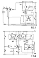
- a video source VS has a first terminal connected to ground Gnd, and a second terminal connected to a signal input SI of a low-voltage differential amplifier AMP through an input resistor Rin.
- An output of the amplifier AMP is connected to emitter terminals of PNP transistors Tr1 and Tr2 forming a first current repeater CR1.
- PNP transistors Tr1 and Tr2 forming a first current repeater CR1.
- the base and collector of transistor Tr1 are connected to the cathode of a PN emitter PNE, whose anode is connected to the collector and base of a NPN transistor Tr3.
- Transistor Tr3 is the input transistor of a second current repeater CR2 whose output transistor is formed by NPN transistor Tr4.
- the emitters of transistors Tr3 and Tr4 are connected to ground Gnd.
- the collectors of transistors Tr2 and Tr4 are interconnected and connected to a feedback input FI of the amplifier AMP. Both the signal input SI and the feedback input FI are connected to a non-inverting input of the differential amplifier AMP.
- the inverting input of the differential amplifier AMP is connected to the middle connection of a resistive divider which consists of the series connection of two resistors R between the output of the amplifier AMP and ground Gnd.
- the circuit works as follows.
- the overall gain is determined by the input resistor Rin. For example, assuming a peak beam current of 4 mA is required, then Rin is 175 Ohm.
- the output voltage Vdrive of the amplifier AMP effectively determines the voltage across the PN emitter PNE, because the anode is a virtual ground at about 0.7 V, while the voltage drop across Tr1 is also about 0.7 V.
- the currents flowing at both ends of the PN emitter PNE, viz. through the transistors Tr1 and Tr3, are mirrored at the collectors of Tr2 and Tr4, respectively.
- the differential current is, in fact, the emission current.
- the differential current, flowing in Tr4 also increases - thus away from the positive node of amplifier AMP - providing negative differential current feedback.
- the resistive divider with the two resistors R effectively fixes the collector potential of the transistors Tr2 and Tr4 at 0.5 * Vdrive + 0.7, thereby allowing sufficient dynamic range for the devices.
- possible errors in the current repeater CR1 i.e. the collector current in Tr1 and Tr2 can be accounted for. The only error then is between current repeater CR1 and current repeater CR2.
- the video source VS supplies an output signal which is the sum of a video signal and an offset voltage.
- This offset voltage serves for blacklevel adjustment and for allowing for possible differences between different emitter characteristics.
- the offset voltage also improves the speed of the device by keeping the device capacitances charged. Typically, the offset voltage will be a relatively small voltage.
- Fig. 2 shows an alternative driver for the PN emitter PNE.
- the differential amplifier AMP comprises two NPN transistors Tr5 and Tr6 whose interconnected emitters are connected to ground Gnd through bias current source BCS.
- a third current repeater CR3 comprises two PNP transistors Tr7 and Tr8. The base and the collector of the input transistor Tr7 are connected to the collector of transistor Tr5. The collector of the output transistor Tr8 of the third current repeater CR3 is connected to the collector of the transistor Tr6, and to the collector and base of an input transistor Tr9 of the first current repeater CR1'.
- the bases of the differential amplifier transistors Tr5 and Tr6 are connected to middle connections of respective resistive dividers.
- Each resistive divider has two equal resistors R.
- the resistive divider at the base of transistor Tr5 is between the supply voltage Vs and ground Gnd.
- the video source VS has one terminal connected to ground Gnd and another terminal connected to the signal input SI of the differential amplifier AMP, i.e. the base of transistor Tr6, through one of the resistive divider resistors R.
Landscapes
- Engineering & Computer Science (AREA)
- Physics & Mathematics (AREA)
- Microelectronics & Electronic Packaging (AREA)
- General Physics & Mathematics (AREA)
- Nonlinear Science (AREA)
- Electromagnetism (AREA)
- Power Engineering (AREA)
- Radar, Positioning & Navigation (AREA)
- Automation & Control Theory (AREA)
- Multimedia (AREA)
- Signal Processing (AREA)
- Amplifiers (AREA)
- Control Of Indicators Other Than Cathode Ray Tubes (AREA)
- Transforming Electric Information Into Light Information (AREA)
Applications Claiming Priority (2)
| Application Number | Priority Date | Filing Date | Title |
|---|---|---|---|
| EP92200831 | 1992-03-23 | ||
| EP92200831 | 1992-03-23 |
Publications (3)
| Publication Number | Publication Date |
|---|---|
| EP0562683A2 EP0562683A2 (en) | 1993-09-29 |
| EP0562683A3 EP0562683A3 (OSRAM) | 1994-02-16 |
| EP0562683B1 true EP0562683B1 (en) | 1997-07-09 |
Family
ID=8210498
Family Applications (1)
| Application Number | Title | Priority Date | Filing Date |
|---|---|---|---|
| EP93200810A Expired - Lifetime EP0562683B1 (en) | 1992-03-23 | 1993-03-19 | A display device having a display tube including a cold cathode |
Country Status (4)
| Country | Link |
|---|---|
| US (1) | US5347197A (OSRAM) |
| EP (1) | EP0562683B1 (OSRAM) |
| JP (1) | JPH0667615A (OSRAM) |
| DE (1) | DE69311940T2 (OSRAM) |
Families Citing this family (4)
| Publication number | Priority date | Publication date | Assignee | Title |
|---|---|---|---|---|
| US6046730A (en) * | 1996-03-15 | 2000-04-04 | At&T Corp | Backlighting scheme for a multimedia terminal keypad |
| US6392355B1 (en) | 2000-04-25 | 2002-05-21 | Mcnc | Closed-loop cold cathode current regulator |
| EP2116671A1 (de) | 2008-05-06 | 2009-11-11 | Bieri Alpha Covers AG | Strebe für eine Schwimmbadabdeckung |
| EP2374964A1 (de) | 2010-04-09 | 2011-10-12 | Bieri Alpha Covers AG | Strebe für eine Schwimmbadabdeckung |
Family Cites Families (5)
| Publication number | Priority date | Publication date | Assignee | Title |
|---|---|---|---|---|
| US4484228A (en) * | 1982-10-14 | 1984-11-20 | Rca Corporation | Signal processing network for an automatic kinescope bias control system |
| US4484229A (en) * | 1982-10-29 | 1984-11-20 | Rca Corporation | Automatic kinescope bias control system with selectively disabled signal processor |
| SU1338110A1 (ru) * | 1985-10-05 | 1987-09-15 | Предприятие П/Я Р-6149 | Видеоусилитель |
| US4829492A (en) * | 1986-07-30 | 1989-05-09 | Woodstream Corporation | Depthfinder with color LCD display |
| US4973890A (en) * | 1990-05-10 | 1990-11-27 | Electrohome Limited | Cascode mirror video amplifier |
-
1993
- 1993-03-19 EP EP93200810A patent/EP0562683B1/en not_active Expired - Lifetime
- 1993-03-19 DE DE69311940T patent/DE69311940T2/de not_active Expired - Fee Related
- 1993-03-19 US US08/035,131 patent/US5347197A/en not_active Expired - Fee Related
- 1993-03-23 JP JP5064226A patent/JPH0667615A/ja active Pending
Also Published As
| Publication number | Publication date |
|---|---|
| DE69311940T2 (de) | 1998-01-22 |
| JPH0667615A (ja) | 1994-03-11 |
| EP0562683A2 (en) | 1993-09-29 |
| US5347197A (en) | 1994-09-13 |
| DE69311940D1 (de) | 1997-08-14 |
| EP0562683A3 (OSRAM) | 1994-02-16 |
Similar Documents
| Publication | Publication Date | Title |
|---|---|---|
| JPH0714131B2 (ja) | 電圧−電流変換器 | |
| JP2542623B2 (ja) | カレントミラ−回路 | |
| EP0131340A1 (en) | Current stabilising circuit | |
| EP0562683B1 (en) | A display device having a display tube including a cold cathode | |
| EP0209334B1 (en) | Current mirror circuit | |
| US5406222A (en) | High gain transistor amplifier | |
| US4013973A (en) | Amplifier arrangement | |
| US6285258B1 (en) | Offset voltage trimming circuit | |
| EP0132863A1 (en) | Protection circuit | |
| EP0448169B1 (en) | Amplifier arrangement | |
| US4247825A (en) | Transistor amplifier | |
| KR950000161B1 (ko) | 증폭기 장치 및 푸시풀 증폭기 | |
| US4573022A (en) | Semiconductor integrated circuit using vertical PNP transistors | |
| US3739292A (en) | Amplifier circuit using complementary symmetry transistors | |
| EP0129936B1 (en) | Current source circuit arrangement | |
| US6246290B1 (en) | High gain, current driven, high frequency amplifier | |
| US3699467A (en) | Bias circuit for a complementary transistor output stage | |
| JP3107590B2 (ja) | 電流極性変換回路 | |
| JP2783301B2 (ja) | アクティブ・フィルタ回路 | |
| JP2547896B2 (ja) | 電流反転回路 | |
| KR840001120B1 (ko) | 증폭기 | |
| JPS593651Y2 (ja) | 垂直偏向装置 | |
| JPS6223612A (ja) | 温度補償型カレントスイツチ回路 | |
| JPH05206759A (ja) | ベース電流補償回路 | |
| JP3116359B2 (ja) | ベース電流補償回路 |
Legal Events
| Date | Code | Title | Description |
|---|---|---|---|
| PUAI | Public reference made under article 153(3) epc to a published international application that has entered the european phase |
Free format text: ORIGINAL CODE: 0009012 |
|
| AK | Designated contracting states |
Kind code of ref document: A2 Designated state(s): DE FR GB |
|
| PUAL | Search report despatched |
Free format text: ORIGINAL CODE: 0009013 |
|
| AK | Designated contracting states |
Kind code of ref document: A3 Designated state(s): DE FR GB |
|
| 17P | Request for examination filed |
Effective date: 19940728 |
|
| GRAG | Despatch of communication of intention to grant |
Free format text: ORIGINAL CODE: EPIDOS AGRA |
|
| 17Q | First examination report despatched |
Effective date: 19960909 |
|
| GRAH | Despatch of communication of intention to grant a patent |
Free format text: ORIGINAL CODE: EPIDOS IGRA |
|
| GRAH | Despatch of communication of intention to grant a patent |
Free format text: ORIGINAL CODE: EPIDOS IGRA |
|
| GRAA | (expected) grant |
Free format text: ORIGINAL CODE: 0009210 |
|
| AK | Designated contracting states |
Kind code of ref document: B1 Designated state(s): DE FR GB |
|
| REF | Corresponds to: |
Ref document number: 69311940 Country of ref document: DE Date of ref document: 19970814 |
|
| ET | Fr: translation filed | ||
| PLBE | No opposition filed within time limit |
Free format text: ORIGINAL CODE: 0009261 |
|
| STAA | Information on the status of an ep patent application or granted ep patent |
Free format text: STATUS: NO OPPOSITION FILED WITHIN TIME LIMIT |
|
| 26N | No opposition filed | ||
| REG | Reference to a national code |
Ref country code: FR Ref legal event code: CD |
|
| PGFP | Annual fee paid to national office [announced via postgrant information from national office to epo] |
Ref country code: FR Payment date: 20000328 Year of fee payment: 8 |
|
| PGFP | Annual fee paid to national office [announced via postgrant information from national office to epo] |
Ref country code: GB Payment date: 20000331 Year of fee payment: 8 |
|
| PGFP | Annual fee paid to national office [announced via postgrant information from national office to epo] |
Ref country code: DE Payment date: 20000524 Year of fee payment: 8 |
|
| PG25 | Lapsed in a contracting state [announced via postgrant information from national office to epo] |
Ref country code: GB Free format text: LAPSE BECAUSE OF NON-PAYMENT OF DUE FEES Effective date: 20010319 |
|
| GBPC | Gb: european patent ceased through non-payment of renewal fee |
Effective date: 20010319 |
|
| PG25 | Lapsed in a contracting state [announced via postgrant information from national office to epo] |
Ref country code: FR Free format text: LAPSE BECAUSE OF NON-PAYMENT OF DUE FEES Effective date: 20011130 |
|
| REG | Reference to a national code |
Ref country code: FR Ref legal event code: ST |
|
| PG25 | Lapsed in a contracting state [announced via postgrant information from national office to epo] |
Ref country code: DE Free format text: LAPSE BECAUSE OF NON-PAYMENT OF DUE FEES Effective date: 20020101 |