EP0556085B1 - Steckverbindung-Zusammenbau zwischen einer Mutterschaltung und einer Tochterschaltung - Google Patents
Steckverbindung-Zusammenbau zwischen einer Mutterschaltung und einer Tochterschaltung Download PDFInfo
- Publication number
- EP0556085B1 EP0556085B1 EP93400249A EP93400249A EP0556085B1 EP 0556085 B1 EP0556085 B1 EP 0556085B1 EP 93400249 A EP93400249 A EP 93400249A EP 93400249 A EP93400249 A EP 93400249A EP 0556085 B1 EP0556085 B1 EP 0556085B1
- Authority
- EP
- European Patent Office
- Prior art keywords
- connector
- insulating body
- connection
- connection assembly
- assembly according
- Prior art date
- Legal status (The legal status is an assumption and is not a legal conclusion. Google has not performed a legal analysis and makes no representation as to the accuracy of the status listed.)
- Expired - Lifetime
Links
- 230000010287 polarization Effects 0.000 claims 1
- 239000012212 insulator Substances 0.000 description 4
- 238000009434 installation Methods 0.000 description 2
- 230000037431 insertion Effects 0.000 description 1
- 238000003780 insertion Methods 0.000 description 1
- 238000004519 manufacturing process Methods 0.000 description 1
Images

Classifications
-
- H—ELECTRICITY
- H01—ELECTRIC ELEMENTS
- H01R—ELECTRICALLY-CONDUCTIVE CONNECTIONS; STRUCTURAL ASSOCIATIONS OF A PLURALITY OF MUTUALLY-INSULATED ELECTRICAL CONNECTING ELEMENTS; COUPLING DEVICES; CURRENT COLLECTORS
- H01R12/00—Structural associations of a plurality of mutually-insulated electrical connecting elements, specially adapted for printed circuits, e.g. printed circuit boards [PCB], flat or ribbon cables, or like generally planar structures, e.g. terminal strips, terminal blocks; Coupling devices specially adapted for printed circuits, flat or ribbon cables, or like generally planar structures; Terminals specially adapted for contact with, or insertion into, printed circuits, flat or ribbon cables, or like generally planar structures
- H01R12/70—Coupling devices
- H01R12/7005—Guiding, mounting, polarizing or locking means; Extractors
-
- Y—GENERAL TAGGING OF NEW TECHNOLOGICAL DEVELOPMENTS; GENERAL TAGGING OF CROSS-SECTIONAL TECHNOLOGIES SPANNING OVER SEVERAL SECTIONS OF THE IPC; TECHNICAL SUBJECTS COVERED BY FORMER USPC CROSS-REFERENCE ART COLLECTIONS [XRACs] AND DIGESTS
- Y10—TECHNICAL SUBJECTS COVERED BY FORMER USPC
- Y10S—TECHNICAL SUBJECTS COVERED BY FORMER USPC CROSS-REFERENCE ART COLLECTIONS [XRACs] AND DIGESTS
- Y10S439/00—Electrical connectors
- Y10S439/948—Contact or connector with insertion depth limiter
Definitions
- the subject of the present invention is a connection set between a motherboard and a card girl.
- a set of connection between a motherboard and a daughterboard comprising a first connector comprising a first insulating body having first elements of contact whose first end is intended to be inserted into a motherboard as well as a second connector comprising a second insulating body having second contact elements including one first end is intended to cooperate with a second end of said contact elements correspondents and a second end of which is intended to be inserted in a daughter card, one side of connection of the first and second insulating body being opposite when the first and the second connector are connected.
- connection set cannot be used only for at most two different card thicknesses girl.
- circuit boards printed in different thicknesses for example 1.6 mm, 2.4 mm, and 3.2 mm. It is not currently possible to treat all possible cases with a single connector width, so that a standardization of models is not possible, hence disadvantages due to the manufacturing costs of connectors of different widths and storage of different types of connectors, which make little interesting the use of such connectors for high thickness printed circuits (3.2 mm in the example above).
- Patent application EP-A-0 392 629 (Van Woensel) describes a example of connection assembly according to known art.
- the subject of the invention is a set of connection of the aforementioned type making it possible to remedy the aforementioned drawback.
- connection assembly is for this purpose characterized in that it comprises a wedging device for maintaining a distance determined between said connection faces of the first and the second insulating body so that a end of daughter board spaced first insulating body, in particular for keeping between the end of the daughter card and the installation plan of the motherboard, a distance equal to the standard dimension connectors of the prior art. Said end of the daughter card is thinned. This allows in particular to separate the second connector from the first connector (male) so that the first row of connection either in one part unthinned daughter card.
- a lateral branch of the first insulating body has at a distal end a housing arranged on its face internal and intended to receive said end thinned, said distance being such that when the first and second connector are connected, an edge of the daughter card is located immediate proximity of said distal end.
- a side face of the second insulating body then has means for holding said end thinned out daughter card.
- the wedging device is also an element of foolproof.
- a timing device may include a patch on at least one said insulating body and / or a projecting element forming an integral part of minus a so-called connection face.
- An insulating body in particular the first body insulator, can have a central part and two lateral branches, the inner side of the part central unit constituting a said connection face.
- Said unthinned edge can be located at immediate proximity of a second end of said connection elements. This keeps a fixation effective of the daughter card on the second body insulating which avoids the constraints on the second ends of the second connection elements.
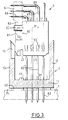
- a connection assembly has a male connector 3 having a body insulator 10 with a flattened U-shaped profile and a female connector 5 having a central body insulator 81.
- the insulating body 10 includes a region central 11 and two lateral branches 12 and 13, the branch referenced 12 comprising means for foolproof.
- the central region 11 has a plurality of contact elements 60 having a region 61 united with the central region 11, a region 63 forcibly inserted ("press-fit") into motherboard 1, and a male contact region 62 projecting from one side connection 31 of the central region 11.
- the insulating central body 81 has contact elements 85 having a region 83 of female contact set back from one face of connection 41 and connection 88 with forced insertion ("press-fit") in a daughter card 2.
- the elements 85 have a bent region 87 arranged in a zone insulating rear 89 of the insulating body 81.
- a pawn of centering and holding 20 carried by a lateral face 82 of the insulating body 81 allows to solarize a end 25 of daughter card 2 with central body insulator 81.
- a housing 16 located at the distal part 17 of branch 12 can receive the end of the pawn 20.
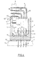
- Figure 2 shows a set of connection which allows, according to the invention, the setting in artwork of a daughter card 6 of greater thickness.
- One or more grooves 42 of the insulating body 81 allow to receive a shim of thickness 40.
- An insert of thickness 40 added is housed removably in the central region 11 or in the central insulating body 81 so that when connectors 3 and 5 are assembled on faces 31 and 41 are spaced from each other. This allows offset the two connectors longitudinally assembled 3 and 5 so that the end 62 of daughter card 6 is spaced from distal end 53 of the arm 12. The position of the end 70 of the card girl remains unchanged.
- the end 61 of the card girl 6 is thinned.
- the proximal part 63 of the end 61 is extended by a connecting edge 62 with the unthinned end 66 of the daughter card 6.
- This end 66 is located in the immediate vicinity of a row 89 of connections 88 and close to the end 53 of the arm 12.
- the shim 40 thus allows to maintain the row 89 of contacts 88 in an unthinned region of the daughter card 6 and at closer to the distal end (here chamfered) of branch 12.
- shim of reported thickness 40 also as a means of coding.
- Keying elements are known, in particular from the request for European patent EP-A-0392629 (Van Woensel) cited above.
- a such wedge is compatible with housing such as 42 (fig. 2 to 4).
- An attached shim 40 makes it possible to adapt easily a standard connection set to all the thicknesses of the daughter card. Additionally, as noted above, it may or may not fulfill a function of keying, which gives great flexibility of use at low cost.
- the shim 44 is an integral part of central region 11 (or of the insulating central body 81). In this case, the whole connection is in principle provided for a thickness maximum given from daughter card 6. It is however possible to also use a shim removable insert to adapt to other daughter card thicknesses 6.
Landscapes
- Coupling Device And Connection With Printed Circuit (AREA)
- Details Of Connecting Devices For Male And Female Coupling (AREA)
Claims (8)
- Verbindungseinheit zwischen einer Mutterleiterplatte (1) und einer Tochterleiterplatte (6) mit einem ersten Stekker (3), der einen ersten Isolator (10) enthält, der erste Anschlußelemente (60) aufweist, deren erstes Ende (63) dazu bestimmt ist, in der Mutterleiterplatte (1) eingeschoben zu werden, einem zweiten Stecker (5), der einen zweiten Isolator (81) enthält, der zweite Anschlußelemente (85) aufweist, deren erstes Ende (83) dazu bestimmt ist mit einem zweiten Ende (62) der entsprechenden ersten Anschlußelemente (60) zusammenzuwirken, und deren zweites Ende (88) dazu bestimmt ist in eine Tochterleiterplatte (6) eingeschoben zu werden, einer Anschlußfläche (31, 41) des ersten (10) und des zweiten (81) Isolators, die gegenüberliegen, wenn der erste (3) mit dem zweiten (5) Stecker verbunden ist, und einem Ende (61) der Tochterleiterplatte (6), das in eine Aufnahme zwischen einer Seitenfläche (82) des zweiten Isolators (81) und eines Seitenarms (12) des ersten Isolators (10) eingeschoben ist,
dadurch gekennzeichnet, daß
er eine Feststellvorrichtung (40, 44) aufweist, die dazu bestimmt ist, einen bestimmten Abstand zwischen den genannten Abschlußflächen (31, 41) des ersten (10) und des zweiten (81) Isolators zu halten, in der Art, daß ein Abstand zwischen einem Ende (61) der Tochterleiterplatte (6) und dem ersten Isolator (10) verbleibt, wobei das genannte Ende (61) der Tochterleiterplatte (6) verjüngt ist, und daß der erwähnte Abstand so bestimmt ist, daß, wenn der erste (3) mit dem zweiten (5) Stecker verbunden ist, der unverjüngte Rand (66) der Tochterleiterplatte (6) in unmittelbarer Nähe des entfernten Ende (53) des Seitenarms (12) des ersten Isolators (10) angeordnet ist. - Verbindungseinheit nach Anspruch 1, dadurch gekennzeichnet, daß die erwähnte Feststellvorrichtung ebenfalls ein vertauschhemmendes Element (40) aufweist.
- Verbindungseinheit nach Anspruch 1 oder 2, dadurch gekennzeichnet, daß die Feststellvorrichtung mindestens ein Aufsteckteil (40) an einem der genannten Isolatoren (10, 81) aufweist.
- Verbindungseinheit nach einem der vorherigen Ansprüche, dadurch gekennzeichnet, daß die Feststellvorrichtung mindestens ein überstehendes Element (44) aufweist, das in mindestens einer der genannten Anschlußflächen (31, 41) integriert ist.
- Verbindungseinheit nach einem der vorhergehenden Ansprüche, dadurch gekennzeichnet, daß ein genannter Isolator (10) einen Mittelteil (11) und zwei Seitenarme (12, 13) aufweist, die Innenfläche des Mittelteils (11) bildet eine genannte Anschlußfläche (31).
- Verbindungseinheit nach einem der vorigen Ansprüche, dadurch gekennzeichnet, daß ein erwähnter Seitenarm (12) an einem entfernten Ende (17) eine Aufnahme (16) darstellt, an der Innenseite angeordnet ist gegenüber dem genannten Ende (61) der Tochterleiterplatte (6), wenn der erste (3) mit dem zweiten (5) Stecker verbunden ist.
- Verbindungseinheit nach einem der vorigen Ansprüche, dadurch gekennzeichnet, daß der unverjüngte Rand (66) in unmittelbarer Nähe des zweiten Ende (88) der erwähnten zweiten Anschlußelemente (85) angeordnet ist.
- Verbindungseinheit nach einem der vorigen Ansprüche, dadurch gekennzeichnet, daß der erste Stecker (3) ein männlicher Stecker ist, und daß der zweite Stecker (5) ein weiblicher Stecker ist.
Applications Claiming Priority (2)
| Application Number | Priority Date | Filing Date | Title |
|---|---|---|---|
| FR9201618A FR2687508B1 (fr) | 1992-02-13 | 1992-02-13 | Ensemble de connexion entre une carte mere et une carte fille. |
| FR9201618 | 1992-02-13 |
Publications (2)
| Publication Number | Publication Date |
|---|---|
| EP0556085A1 EP0556085A1 (de) | 1993-08-18 |
| EP0556085B1 true EP0556085B1 (de) | 1998-04-29 |
Family
ID=9426607
Family Applications (1)
| Application Number | Title | Priority Date | Filing Date |
|---|---|---|---|
| EP93400249A Expired - Lifetime EP0556085B1 (de) | 1992-02-13 | 1993-02-02 | Steckverbindung-Zusammenbau zwischen einer Mutterschaltung und einer Tochterschaltung |
Country Status (4)
| Country | Link |
|---|---|
| US (1) | US5443401A (de) |
| EP (1) | EP0556085B1 (de) |
| DE (1) | DE69318199T2 (de) |
| FR (1) | FR2687508B1 (de) |
Families Citing this family (9)
| Publication number | Priority date | Publication date | Assignee | Title |
|---|---|---|---|---|
| US5443398A (en) * | 1994-01-31 | 1995-08-22 | Robinson Nugent, Inc. | Inverse backplane connector system |
| US6551123B1 (en) * | 1995-02-10 | 2003-04-22 | Marquardt Gmbh | Guiding arrangement for a plug-in battery pack operating an electric appliance |
| TW491425U (en) * | 2000-12-21 | 2002-06-11 | Hon Hai Prec Ind Co Ltd | Electrical connector assembly with a device for preventing erroneous insertion |
| US6910897B2 (en) | 2001-01-12 | 2005-06-28 | Litton Systems, Inc. | Interconnection system |
| US6843657B2 (en) | 2001-01-12 | 2005-01-18 | Litton Systems Inc. | High speed, high density interconnect system for differential and single-ended transmission applications |
| US6979202B2 (en) | 2001-01-12 | 2005-12-27 | Litton Systems, Inc. | High-speed electrical connector |
| US6592382B2 (en) | 2001-12-17 | 2003-07-15 | Woody Wurster | Simplified board connector |
| US6884091B1 (en) * | 2004-04-19 | 2005-04-26 | Component Equipment Company, Inc. | Electrical connector assembly |
| US8690588B2 (en) * | 2011-12-20 | 2014-04-08 | Yazaki North America, Inc. | Junction box assembly having an over-travel spring |
Family Cites Families (12)
| Publication number | Priority date | Publication date | Assignee | Title |
|---|---|---|---|---|
| US3614714A (en) * | 1969-11-21 | 1971-10-19 | Rca Corp | Edge connector with polarizing member |
| JPS5828717B2 (ja) * | 1979-08-31 | 1983-06-17 | 富士通株式会社 | 極性付コネクタ |
| US4531795A (en) * | 1983-03-01 | 1985-07-30 | Aries Electronics, Inc. | Ejector socket for DIP jumpers |
| FR2553588B1 (fr) * | 1983-10-14 | 1986-01-03 | Telecommunications Sa | Dispositif de connexion pour test de circuit imprime |
| US4533203A (en) * | 1983-12-07 | 1985-08-06 | Amp Incorporated | Connector for printed circuit boards |
| JPS6197557A (ja) * | 1984-10-19 | 1986-05-16 | Kawasaki Steel Corp | 二次イオン質量分析装置 |
| DE3603250A1 (de) * | 1986-02-03 | 1987-08-06 | Allied Corp | Steckverbinder, isolierkoerper dafuer und verfahren zur befestigung des steckverbinders an einer leiterplatte |
| US4773881A (en) * | 1987-05-21 | 1988-09-27 | Amp Incorporated | Keying system for connector assemblies |
| NL8900947A (nl) * | 1989-04-14 | 1990-11-01 | Du Pont Nederland | Connectorsamenstel. |
| EP0397057B1 (de) * | 1989-05-12 | 1994-07-27 | Siemens Aktiengesellschaft | Anordnung zur mechanischen und elektrischen Verbindung einer Ergänzungsleiterplatte an einer Grundleiterplatte |
| JPH0388289A (ja) * | 1989-08-31 | 1991-04-12 | Fujitsu Ltd | プリント配線板用コネクタ |
| FR2685556B1 (fr) * | 1991-12-23 | 1994-03-25 | Souriau & Cie | Element modulaire de connexion electrique. |
-
1992
- 1992-02-13 FR FR9201618A patent/FR2687508B1/fr not_active Expired - Fee Related
-
1993
- 1993-02-02 DE DE69318199T patent/DE69318199T2/de not_active Expired - Fee Related
- 1993-02-02 EP EP93400249A patent/EP0556085B1/de not_active Expired - Lifetime
-
1994
- 1994-10-27 US US08/331,143 patent/US5443401A/en not_active Expired - Fee Related
Also Published As
| Publication number | Publication date |
|---|---|
| DE69318199D1 (de) | 1998-06-04 |
| DE69318199T2 (de) | 1998-10-22 |
| FR2687508B1 (fr) | 1994-11-04 |
| EP0556085A1 (de) | 1993-08-18 |
| FR2687508A1 (fr) | 1993-08-20 |
| US5443401A (en) | 1995-08-22 |
Similar Documents
| Publication | Publication Date | Title |
|---|---|---|
| EP0556085B1 (de) | Steckverbindung-Zusammenbau zwischen einer Mutterschaltung und einer Tochterschaltung | |
| EP0649195B1 (de) | Verbindungselement mit Isoliergehäuse | |
| EP0635167B1 (de) | Trennbarer steckverbinder für kommunikationsnetz | |
| AU711843B2 (en) | A coaxial connector and method for fixing this connector to a circuit board | |
| EP0123590A1 (de) | Verbinder | |
| FR2814858A1 (fr) | Connecteur a ressort pour la connexion electrique de pistes d'un ecran d'affichage avec un circuit electrique | |
| EP1028490A1 (de) | Koaxialverbinder zum Verbinden von zwei Leiterplatten | |
| FR2502407A1 (fr) | Dispositif de maintien et de guidage pour broches coudees de connecteur | |
| FR2509538A1 (fr) | Boite de connexion electrique | |
| FR2484718A3 (fr) | Ensemble a connecteur electrique et a dispositif pour soulager les fils des contraintes | |
| EP0596776A1 (de) | Kontaktleiste mit anpassbarer Etikettierung | |
| FR2750261A1 (fr) | Structure de connexion pour un corps de circuit plat et un connecteur | |
| FR2859826A1 (fr) | Connecteur de carte a memoire pour un montage sur une plaquette a circuit imprime | |
| EP0738983B1 (de) | Elektrischer Verbinder für eine Kontaktkarte mit integrierten Schaltungen | |
| AU724160B2 (en) | Board mounted electrical connector with improved retention means | |
| EP0593336B1 (de) | Lösbare Befestigung zum Verbinden einer Trägerplatte mit einem Bauelement und Verbinder mit einer solchen Befestigung | |
| JP3358156B2 (ja) | 可動コネクタへの挿着用コネクタ | |
| FR2779013A1 (fr) | Clip soudable pour connecteur a contacts coudes | |
| FR2602920A1 (fr) | Connecteur a filtre d'attenuation incorpore | |
| EP3003743A2 (de) | Elektronische verbindungsvorrichtung für eine fahrzeuganhängerkupplung | |
| US6093065A (en) | Electrical wedge connector having sleeve with wedge locking tabs | |
| EP0247945B1 (de) | Elektrische Steckvorrichtung zwischen zwei Teilen, hauptsächlich für die Versorgung von Logometern in Kraftfahrzeugen | |
| EP0674357B1 (de) | Gehäuseteilen von elektrischen Verbindern | |
| FR2648665A1 (fr) | Systeme de connexion | |
| EP0511077B1 (de) | Elektrischer Verbinder zum Fixieren und Verbinden von Tochter-Mutterleiterplatten |
Legal Events
| Date | Code | Title | Description |
|---|---|---|---|
| PUAI | Public reference made under article 153(3) epc to a published international application that has entered the european phase |
Free format text: ORIGINAL CODE: 0009012 |
|
| AK | Designated contracting states |
Kind code of ref document: A1 Designated state(s): BE DE ES GB IT NL SE |
|
| 17P | Request for examination filed |
Effective date: 19931029 |
|
| 17Q | First examination report despatched |
Effective date: 19950621 |
|
| GRAG | Despatch of communication of intention to grant |
Free format text: ORIGINAL CODE: EPIDOS AGRA |
|
| GRAG | Despatch of communication of intention to grant |
Free format text: ORIGINAL CODE: EPIDOS AGRA |
|
| GRAH | Despatch of communication of intention to grant a patent |
Free format text: ORIGINAL CODE: EPIDOS IGRA |
|
| GRAH | Despatch of communication of intention to grant a patent |
Free format text: ORIGINAL CODE: EPIDOS IGRA |
|
| GRAA | (expected) grant |
Free format text: ORIGINAL CODE: 0009210 |
|
| AK | Designated contracting states |
Kind code of ref document: B1 Designated state(s): BE DE ES GB IT NL SE |
|
| PG25 | Lapsed in a contracting state [announced via postgrant information from national office to epo] |
Ref country code: GB Free format text: LAPSE BECAUSE OF FAILURE TO SUBMIT A TRANSLATION OF THE DESCRIPTION OR TO PAY THE FEE WITHIN THE PRESCRIBED TIME-LIMIT Effective date: 19980429 Ref country code: ES Free format text: THE PATENT HAS BEEN ANNULLED BY A DECISION OF A NATIONAL AUTHORITY Effective date: 19980429 |
|
| REF | Corresponds to: |
Ref document number: 69318199 Country of ref document: DE Date of ref document: 19980604 |
|
| ITF | It: translation for a ep patent filed | ||
| PG25 | Lapsed in a contracting state [announced via postgrant information from national office to epo] |
Ref country code: SE Free format text: LAPSE BECAUSE OF FAILURE TO SUBMIT A TRANSLATION OF THE DESCRIPTION OR TO PAY THE FEE WITHIN THE PRESCRIBED TIME-LIMIT Effective date: 19980729 |
|
| GBV | Gb: ep patent (uk) treated as always having been void in accordance with gb section 77(7)/1977 [no translation filed] |
Effective date: 19980429 |
|
| PLBE | No opposition filed within time limit |
Free format text: ORIGINAL CODE: 0009261 |
|
| STAA | Information on the status of an ep patent application or granted ep patent |
Free format text: STATUS: NO OPPOSITION FILED WITHIN TIME LIMIT |
|
| 26N | No opposition filed | ||
| PGFP | Annual fee paid to national office [announced via postgrant information from national office to epo] |
Ref country code: NL Payment date: 20010228 Year of fee payment: 9 |
|
| PGFP | Annual fee paid to national office [announced via postgrant information from national office to epo] |
Ref country code: BE Payment date: 20020221 Year of fee payment: 10 |
|
| PGFP | Annual fee paid to national office [announced via postgrant information from national office to epo] |
Ref country code: DE Payment date: 20020430 Year of fee payment: 10 |
|
| PG25 | Lapsed in a contracting state [announced via postgrant information from national office to epo] |
Ref country code: NL Free format text: LAPSE BECAUSE OF NON-PAYMENT OF DUE FEES Effective date: 20020901 |
|
| NLV4 | Nl: lapsed or anulled due to non-payment of the annual fee |
Effective date: 20020901 |
|
| PG25 | Lapsed in a contracting state [announced via postgrant information from national office to epo] |
Ref country code: BE Free format text: LAPSE BECAUSE OF NON-PAYMENT OF DUE FEES Effective date: 20030228 |
|
| PG25 | Lapsed in a contracting state [announced via postgrant information from national office to epo] |
Ref country code: DE Free format text: LAPSE BECAUSE OF NON-PAYMENT OF DUE FEES Effective date: 20030902 |
|
| PG25 | Lapsed in a contracting state [announced via postgrant information from national office to epo] |
Ref country code: IT Free format text: LAPSE BECAUSE OF NON-PAYMENT OF DUE FEES;WARNING: LAPSES OF ITALIAN PATENTS WITH EFFECTIVE DATE BEFORE 2007 MAY HAVE OCCURRED AT ANY TIME BEFORE 2007. THE CORRECT EFFECTIVE DATE MAY BE DIFFERENT FROM THE ONE RECORDED. Effective date: 20050202 |