EP0555659B1 - Module à multi-puce - Google Patents
Module à multi-puce Download PDFInfo
- Publication number
- EP0555659B1 EP0555659B1 EP93100658A EP93100658A EP0555659B1 EP 0555659 B1 EP0555659 B1 EP 0555659B1 EP 93100658 A EP93100658 A EP 93100658A EP 93100658 A EP93100658 A EP 93100658A EP 0555659 B1 EP0555659 B1 EP 0555659B1
- Authority
- EP
- European Patent Office
- Prior art keywords
- circuit
- package
- planar
- spacer
- high density
- Prior art date
- Legal status (The legal status is an assumption and is not a legal conclusion. Google has not performed a legal analysis and makes no representation as to the accuracy of the status listed.)
- Expired - Lifetime
Links
Images


Classifications
-
- H—ELECTRICITY
- H05—ELECTRIC TECHNIQUES NOT OTHERWISE PROVIDED FOR
- H05K—PRINTED CIRCUITS; CASINGS OR CONSTRUCTIONAL DETAILS OF ELECTRIC APPARATUS; MANUFACTURE OF ASSEMBLAGES OF ELECTRICAL COMPONENTS
- H05K7/00—Constructional details common to different types of electric apparatus
- H05K7/14—Mounting supporting structure in casing or on frame or rack
- H05K7/1422—Printed circuit boards receptacles, e.g. stacked structures, electronic circuit modules or box like frames
- H05K7/1427—Housings
- H05K7/1429—Housings for circuits carrying a CPU and adapted to receive expansion cards
-
- H—ELECTRICITY
- H01—ELECTRIC ELEMENTS
- H01L—SEMICONDUCTOR DEVICES NOT COVERED BY CLASS H10
- H01L23/00—Details of semiconductor or other solid state devices
- H01L23/34—Arrangements for cooling, heating, ventilating or temperature compensation ; Temperature sensing arrangements
- H01L23/46—Arrangements for cooling, heating, ventilating or temperature compensation ; Temperature sensing arrangements involving the transfer of heat by flowing fluids
- H01L23/467—Arrangements for cooling, heating, ventilating or temperature compensation ; Temperature sensing arrangements involving the transfer of heat by flowing fluids by flowing gases, e.g. air
-
- H—ELECTRICITY
- H01—ELECTRIC ELEMENTS
- H01L—SEMICONDUCTOR DEVICES NOT COVERED BY CLASS H10
- H01L25/00—Assemblies consisting of a plurality of individual semiconductor or other solid state devices ; Multistep manufacturing processes thereof
- H01L25/03—Assemblies consisting of a plurality of individual semiconductor or other solid state devices ; Multistep manufacturing processes thereof all the devices being of a type provided for in the same subgroup of groups H01L27/00 - H01L33/00, or in a single subclass of H10K, H10N, e.g. assemblies of rectifier diodes
- H01L25/10—Assemblies consisting of a plurality of individual semiconductor or other solid state devices ; Multistep manufacturing processes thereof all the devices being of a type provided for in the same subgroup of groups H01L27/00 - H01L33/00, or in a single subclass of H10K, H10N, e.g. assemblies of rectifier diodes the devices having separate containers
- H01L25/105—Assemblies consisting of a plurality of individual semiconductor or other solid state devices ; Multistep manufacturing processes thereof all the devices being of a type provided for in the same subgroup of groups H01L27/00 - H01L33/00, or in a single subclass of H10K, H10N, e.g. assemblies of rectifier diodes the devices having separate containers the devices being of a type provided for in group H01L27/00
-
- H—ELECTRICITY
- H01—ELECTRIC ELEMENTS
- H01L—SEMICONDUCTOR DEVICES NOT COVERED BY CLASS H10
- H01L2225/00—Details relating to assemblies covered by the group H01L25/00 but not provided for in its subgroups
- H01L2225/03—All the devices being of a type provided for in the same subgroup of groups H01L27/00 - H01L33/648 and H10K99/00
- H01L2225/10—All the devices being of a type provided for in the same subgroup of groups H01L27/00 - H01L33/648 and H10K99/00 the devices having separate containers
- H01L2225/1005—All the devices being of a type provided for in the same subgroup of groups H01L27/00 - H01L33/648 and H10K99/00 the devices having separate containers the devices being of a type provided for in group H01L27/00
-
- H—ELECTRICITY
- H01—ELECTRIC ELEMENTS
- H01L—SEMICONDUCTOR DEVICES NOT COVERED BY CLASS H10
- H01L2924/00—Indexing scheme for arrangements or methods for connecting or disconnecting semiconductor or solid-state bodies as covered by H01L24/00
- H01L2924/0001—Technical content checked by a classifier
- H01L2924/0002—Not covered by any one of groups H01L24/00, H01L24/00 and H01L2224/00
Definitions
- This invention relates to microelectronic packaging and, more particularly, to a high density, multi-chip package having improved heat dissipation characteristics.
- DRAM dynamic random access memory chips
- DRAM chips have traditionally been packaged as single chip modules. That is, a single silicon die has been wire bonded to a lead frame containing wiring that fans out the necessary signals to and from the chip via a set of individual metal leads. Those leads are then connected to an underlying circuit board.
- the lead frame and silicon chip are usually encased in an epoxy block, from which the individual metal leads extend, such package generally being referred to as a wire bond package.
- the chips are subjected to a process known as burn-in, whereby they are operated for many hours at elevated temperatures and voltages.
- burn-in a process known as burn-in, whereby they are operated for many hours at elevated temperatures and voltages.
- Packaged chips which survive the burn-in operation are then assembled into groups of chips which, in turn, are assembled into groups of groups, etc.
- other components of the memory system such as control logic, error correction logic, etc., are added to the package. Characteristically, such packaging results in large and cumbersome systems which are not suitable for the highest performance DRAM memories.
- a preferred method for interconnecting DRAM chips is via a flexible, thin, insulating carrier that is provided with personalized conductive layers on its opposing surfaces.
- Such packaging is inherently inexpensive and lends itself, readily, to automated bonding processes.
- via-holes are to be avoided in such flexible carriers as they add unnecessary expense.
- some method must be provided to enable communication to the conductive layer that is present on the far side of the insulating carrier.
- U.S. Patent 4,771,366 a plurality of parallel-oriented ceramic card assemblies with interspersed cold plates are described. Each ceramic card has a number of chips mounted on both of its sides, which chips are enclosed by conductive caps that, in turn, bear upon the cold plates.
- U.S. Patent 4,841,355 a high density package is shown having internal pathways for a liquid coolant flow.
- U.S. Patent 3,372,310 a high density package is shown wherein a plurality of chips are mounted on a substrate, an apertured spacer emplaced thereover, and the entire configuration is enclosed within metallic coverplates.
- US-A-3 833 836 discloses a high density package comprising two printed circuit board sandwiched between two metallic plates.
- a high density package for a plurality of integrated circuit chips is described, the package including a number of planar subunits.
- a subunit includes first and second planar metal plates and a spacer metal plate sandwiched therebetween. Each spacer metal plate is provided with a plurality of circuit-receiving apertures.
- a planar circuit carrier is provided for each aperture in the spacer metal plate. One face of each circuit carrier includes a plurality of bonded chips. Each circuit carrier is positioned in a circuit-receiving aperture so that rear aspects of the bonded chips bear upon the second planar metal plate.
- Each circuit carrier has a connector region which extends out from between the first planar metal plate and the metal spacer plate at one extremity of each circuit-receiving aperture.
- a circuit card is positioned at that extremity and has a plurality of interconnection areas, one for each extended connector region. The circuit card has its major surface oriented parallel to the metal plates so that the entire package presents an overall planar configuration.
- this invention provides a high density electronic package that is adapted to contain a plurality of different types of basic circuit packages.
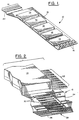
- Fig. 1 a perspective view is shown of a multi-chip, thin film, planar circuit carrier 10.
- the invention will be described in the context of a DRAM package. However, it is to be understood that the package concepts described herein are equally applicable to other integrated circuit applications.
- Circuit carrier 10 comprises a thin film circuit strip 12 which is provided with metalization on both of its sides.
- a plurality of DRAM chips 14 are mounted on one side of circuit strip 12, as are a plurality of surface-mount decoupling capacitors 16.
- At one extremity of circuit carrier 10 is a connector region 18 that is offset to one side of the main axis of circuit strip 12 and is also bent upwardly by a bend at region 20.
- other circuit strips 10 are provided with identical connector regions 18 which are offset to the other side of the main axis of circuit strip 12.
- the first strip in the stack will have its connector region offset to one side of the main axis, whereas the second strip will have its connector region offset to the other side, so that both connector regions can make contact to differing areas of the-same side of a circuit board and not overlap one another.
- FIG. 2 a perspective view of circuit carrier 10 is shown with a DRAM package 14 removed therefrom.
- Circuit strip 12 has metalization on both of its sides, with one side (e.g. 24) being “personalized” in accordance with required circuit details and metalization layer 26, on the opposite side, being substantially continuous as a ground plane.
- flexible circuit strip 12 comprises an upper, personalized, metalization layer 24 and a lower continuous ground plane layer 26. The two layers are separated by a polymer layer 34.
- a solder mask 36 (Fig. 3b) is emplaced over the upper surface of flexible circuit strip 12.
- Each of openings 38 and 40 in solder mask 36 have their size precalculated, in conjunction with the solder receiving volumes communicating therewith, so that after reflow, all solder bumps will be of approximately the same height.
- opening 40 does not extend across the full width of underlying circuit land 42 to control the amount of solder deposited therein, while the width of opening 38 is larger than the opening of hole 44 in polyimid layer 34, to allow more solder to be emplaced therein.
- solder is shown having been deposited on solder mask 36 and into holes 38, 40, etc.
- solder mask is shown having been removed, and in Fig. 3(e), the deposited solder bumps are subjected to a reflow procedure which, in accordance with the above teachings, causes the various bumps to assume a relatively uniform, planar upper surface for subsequent connection to the beam leads of a DRAM package.
- connecting leads would be placed over the solder bumps before reflow, so that bonding could occur simultaneously. Those leads are omitted in Fig. 3.
- an additional polyimid layer 41 (or other dielectric layer)may be emplaced over ground plane 26 to provide an insulating backing therefor.
- Figs. 4, 5, and 6 the incorporation of a plurality of assembled, flexible circuit strips 10 into a heat-sinked package embodying the invention is shown.
- Fig. 4 the various portions of the package will be described starting with the coverplate at the lower left of Fig. 4 and proceeding to the opposing coverplate of the upper right of Fig. 4.
- cover and spacer plates to be hereinafter described are preferably composed of the same, high thermal conductivity metal.
- Preferred materials are copper and aluminum.
- Coverplate 50 has a plurality of airflow passages 52 formed therein. Additionally, a plurality of screw holes 54 enable screws to be inserted to hold the package together.
- Four flexible circuit strips 10, each one holding five DRAM memory chips and associated decoupling capacitors are positioned within apertures in spacer plate 56.
- Spacer plate 56 is provided with four circuit-receiving apertures 58, each one adapted to receive a thin film circuit strip 10. At the bottom of each aperture 58, a portion of spacer plate 56 is thinned so as to provide a space 60 where the connector region of flexible circuit carrier 10 can exit when cover plate 50 is in place.
- Spacer plate 56 is provided with a plurality of airflow apertures 62 which mate with apertures 52 in cover plate 50.
- a second cover plate 64 abuts the right side of spacer plate 56 and is also provided with mating airflow passages 66.
- Cover plates 50, 64, spacer plate 56, and circuit carriers 10 provide a basic subunit of the package. Initially, cover plate 64 is placed beneath spacer plate 56, and then each of circuit carriers 10 is laid in a mating aperture 58. The thickness of spacer plate 56 is made approximately equal to the thickness of circuit carriers 10 (along with their mounted components). Thus, when cover plate 50 is assembled onto the left face of spacer plate 56, physical contact occurs between the rear aspects of each of circuit carriers 10 and solid surface areas of cover plate 50. The frontal aspects of each of the circuit components on circuit carrier 10 contact the solid surface areas of the left side of cover plate 64.
- each circuit carrier 10 a thin sheet of an elastomeric material can be placed behind each circuit carrier 10, so that when the package is assembled, the material is compressed and forces the frontal aspects of the circuit components against cover plate 64.
- Each of the airflow passages in the respective cover plates and spacer plate align with each other and create a smooth, continuous through-passage for airflow. Since each of these passages is continuous, the airflow therein will be laminar and non-turbulent at relatively low flow rates.
- a next subunit is constructed immediately adjoining the first subunit.
- a plurality of circuit carriers 10' are emplaced in mating apertures within an additional spacer plate 70.
- spacer plate 70 Located adjacent the right side of spacer plate 70 is another cover plate 72.
- the connector portions of circuit carriers 10' are oriented to the right side of the carriers axes, whereas the connector portions of circuit carriers 10 are oriented to the left.
- connector portions on circuit carriers 10' make connection to interconnection lands 74 on circuit board 76, whereas connector portions of circuit carriers 10 make connection with interconnection lands 78 on circuit board 76.
- cover plate 50, spacer plate 56, cover plate 64, spacer plate 70 and cover plate 72 are abutted, one against another and are screwed together, with circuit carriers 10 and 10' in place.
- An identical mirror-image package is then assembled and abutted to the aforesaid package.
- Interconnections are then made to circuit card 76 and opposed coverplates 50 and 80 are fastened to abutments 82 and 84 on circuit card 76 to complete the assembly of the package.
- the above assembly procedure is merely exemplary and other assembly sequences may be substituted, depending upon the sophistication of the assembly tooling.
- Fig. 5 the completely assembled package is shown with portions of coverplate 50 and circuit strips 10 removed to show internal details.
- a plurality of decoding or other logic circuits 90 are mounted on circuit board 76 and make interconnection with circuit carriers 10, 10' etc. through wiring (not shown) on and within circuit board 76.
- a plurality of pluggable land areas 92 provide interconnection to circuit board 76 when the package is plugged into a "mother board”.
- Fig. 6 a sectional view of Fig. 5 is shown taken along line 5-5.
- FIG. 7 details are illustrated of an interconnection technique between a decoupling capacitor, circuit strip and a memory chip module that exhibits very low inductance.
- the exploded view shows how connections are made to input/output pins 102 located along the centerline of chip module 100.
- Two layers of wiring 104 and 106 are separated by an insulating sheet 108 that is part of tape 126.
- the top surface wiring 106 contains all of the signal lines for chip module 100, as well as power and ground taps 109 and 110 respectively.
- the bottom surface wiring 104 is used for power and ground distribution. Electrical contact is made between the power and ground taps 109 and 110 and the power and ground distribution lines, respectively, on the bottom surface wiring 104 through a pair of via holes 112 and 114 in insulating sheet 108.
- a surface mount decoupling capacitor 116 whose contact regions 118 and 120 have a paste solder applied.
- the solder bonds capacitor 116 to pads 122 and 124.
- the solder flows up therethrough, through holes 112 and 114 in sheet 108 and bonds to upper wiring bonding pads 109 and 110.
- the thus-bonded chip/capacitor structure may be separated from tape 126 and applied to a circuit carrier 12, as shown in Fig. 1.
- the same structure and procedure may be applied to circuit carrier 12 (instead of tape 126) so that the above-described interconnections are made at the same time chip-to-carrier reflow occurs.
- a pair of DRAM chip modules 130 and 132 may be mounted on adjoining lead frames 134 and 136 respectively.
- capacitor 138 is connected to adjacent bonding pads 140 and 142 to form a bridge therebetween.
- capacitor 138 can be common to modules 130 and 132 since they do not operate at the same time.
- frames 134 and 136 are substantially mirror images of each other. The two wiring halves (left and right) are thus joined by bonding pads 134 and 136, both electrically and mechanically, to the common decoupling capacitor through the bonding solder.
- FIG. 9 a rear view of an 11-chip flexible circuit strip 152 is shown.
- An opening 150 is provided in circuit strip 152 immediately beneath the central input/output contacts on the bottom of each DRAM chip 154.
- Apertures 150 are provided to enable a hot air blast to be directed at the contact region so as to enable solder reflow therein. Subsequent to solder joining, an encapsulant is placed within apertures 150 to create a seal and to prevent solder fatigue.
- FIG. 10 a plan view is shown of four circuit strips 152 that are mounted so that the uppermost surfaces of hidden chip modules 154 bear upon cover plate 158. Cover plate 158 has a multiplicity of airflow holes 160. Connector regions 161 of circuit strips 152 connect to inter-connection lands on multilayer printed circuit board 162.
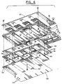
- Fig. 11 the remainder of the circuit package is shown in exploded form, with circuit strips 152 and circuit board 162 removed.
- cover plate 158 is positioned in the middle of the package and is sandwiched between two spacer plates 164 and 166. A further pair of cover plates 168 and 170 are positioned to sandwich the entire structure therebetween.
- Spacer plates 164 and 166 are each provided with apertures 172 for receiving circuit strips 152.
- spacer plates 164 and 166 are largely skeletal and their apertures for airflow are not directly aligned with apertures 160 in the respective cover-plates.
- turbulent airflow occurs within the interior of the package, thereby enabling higher efficiency cooling to occur of the circuit modules contained therein.
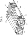
- a completely assembled turbulent airflow package is shown with coverplate 168 and spacer 164 removed. It is to be noted that each of printed boards 162 plugs into a female connector 176 mounted on the rear of a mother board 180. Additional components 182 may be mounted on the underside of mother board 180. When coverplate 168 is in place (see Fig. 5), it extends down and contacts the upper surfaces of logic circuits 90. The heat emanating therefrom is thus conducted upwardly towards apertures 160 for dissipation. Additionally, airflow from the same source that is directed through apertures 160 can also be passed over the underside of mother board 180 to cool the components mounted thereon.
- Fig. 13 a package substantially similar to that of Fig. 12 is shown, however in this instance, the memory package is destined for use with a lower power-dissipation system.
- the memory package is destined for use with a lower power-dissipation system.
- internal airflow passages are not required, and heat generated inside the package is conducted away by the cover and spacer plates to the surface of the package. Airflow across the surface of the package is then sufficient to dissipate the expended power.
- the structure of the package shown in Fig. 13 is much the same as that shown in Fig. 4.
- the circuit package of Fig. 13 has been modified to exhibit a lower overall height. Just above points of interconnection 200 to circuit board 76, the circuit strips, spacer and cover plates have been bent 180 o back over circuit board 76. This enables the package to exhibit a "fatter" but lower-in-height form factor and is particularly useful for highly dense, low power dissipation package configurations.
- a heat conducting insert or gel 202 enables thermal contact between logic circuit 90 and a cover plate of the package.
- the circuit packages of Figs. 13 and 14 are adapted for inclusion in portable equipment where forced air cooling is not available. In such equipment, the cover plate is placed in contact with the outer shell of the equipment to enhance external heat dissipation.
- a high density circuit packaging system has been described that enables brick-like packing of circuit-containing modules on a face-to-face basis.
- the package depending upon expected power dissipation, can be cooled via internal laminar airflow, internal turbulent airflow, external airflow only or other cooling mechanisms.
- the package exhibits excellent EMI radiation characteristics.
- a high density memory module 204 (including at least a plurality of packages 206, in accordance with the invention) is mounted on a base plate 208, along with a number of battery packs 210 which are arranged in an array which naturally matches the geometry of packages 206.
- the spaces between the battery packs 210 act as both a cooling channel for the batteries themselves, and as natural passages for the air required to cool the memory packages.
- the air is forced into the channels by a fan 214.
- the batteries can be either rectangular as shown (as is the case for certain lead-acid and Ni-Cd batteries) or stacks of cylindrical batteries which are available in a wide variety of sizes.
- the cooling air is directed into an array of thin columns.
- the columns are approximately 10 mm wide while the space between columns is approximately 20 mm. These columns are aligned with air flow openings in the packages.
- a separate fan 216 may be used to provide cooling to associated circuit boards 218 having control circuits thereon.
Claims (14)
- Boîtier d'implantation de forte densité pour plusieurs puces à circuit intégré, comprenant:un premier (50) et un second (64) plateaux métalliques plans;un plateau métallique d'écartement (56) intercalé entre les dits premier et second plateaux métalliques plans, plusieurs ouvertures (58) destinées à recevoir un circuit étant pratiquées dans le dit plateau métallique intercalaire;plusieurs supports plans pour circuit (10), une face de chacun des dits supports pour circuit incluant plusieurs puces fixées ("bondées") (14), chacun des dits supports pour circuit est positionné dans une ouverture du dit plateau métallique intercalaire destinée à recevoir un circuit, chacun des dits supports plans pour circuit ayant une région de connexion (18) qui dépasse d'entre le dit premier plateau métallique et le dit plateau métallique intercalaire à une extrémité d'une dite ouverture destinée à recevoir un circuit; etune carte à circuits imprimés (76) placée à la dite extrémité et munie de plusieurs zones d'interconnexion (74, 78), une pour chaque région de connexion étendue, la surface supérieure de la dite carte à circuits étant positionnée parallèlement aux dits premier et second plateaux métalliques, par quoi le dit boîtier présente une configuration globale plane.
- Boîtier d'implantation de forte densité tel que revendiqué dans la revendication 1, où sont des ouvertures pour l'écoulement de l'air(52, 62, 66) sont pratiquées dans chacun des dits premier (50) et second (64) plateaux métalliques plans et le dit plateau métallique intercalaire (56), de sorte que lorsque les dits plateaux sont assemblés pour créer un ensemble unitaire à configuration planaire, les ouvertures dans chacun des dits plateaux sont à la fois alignées et aboutées les unes aux autres de manière à créer des passages pour l'écoulement de l'air qui permettent un écoulement laminaire de l'air au-travers de l'ensemble.
- Boîtier d'implantation de forte densité tel que revendiqué dans la revendication 1, où les dits premier et second plateaux plans métallisés comprennent des passages pour l'écoulement de l'air (52, 66) ayant une section transversale et, où le dit plateau d'écartement en métal est également muni d'ouvertures (62) pour le passage de l'air, mais d'une section transversale plus large, de sorte que lorsque tous les dits plateaux métalliques sont arrangés ensemble en sandwich, il se forme des canaux d'écoulement de l'air ayant des parois intérieures discontinues à cause des différences qui existent entre les différentes sections transversales, canaux au moyen desquels on obtient un écoulement d'air turbulent à l'intérieur du dit boîtier.
- Boîtier d'implantation de forte densité tel que revendiqué dans la revendication 2 ou 3 comprenant en outre une plaquette de circuits imprimés (208) qui possède plusieurs connecteurs parallèles, chaque connecteur placé de manière à recevoir et à s'interconnecter à une carte à circuits, les dits connecteurs étant arrangés de manière à ce que chacune des dites cartes à circuits, une fois insérée, place les dites ouvertures conçues pour l'écoulement de l'air dans une position coaxiale aux ouvertures de circulation de l'air associées à d'autres cartes à circuits imprimés, par quoi la circulation de l'air peut s'effectuer au-travers de toutes les ouvertures alignées coaxialement, sans obstruction.
- Boîtier d'implantation de forte densité tel que revendiqué dans la revendication 1 comprenant en outre:un troisième plateau métallique plan (72);un second plateau intercalaire en métal (70) disposé en sandwich entre le dit troisième plateau métallique plan et le dit second plateau métallique plan; etdes supports de circuits plans (10') placés dans les ouvertures destinées à recevoir les circuits dans le dit second plateau intercalaire métallique et, positionnés de manière à ce que les côtés arrière des puces fixées sur les dits supports soient en contact avec le dit troisième plateau métallique.
- Boîtier d'implantation de forte densité tel que revendiqué dans la revendication 5, où le dit boîtier comprend en outre un image symétrique des dits premier, second et troisième plateaux métalliques plans et des dits premier et second plateaux intercalaires en métal, avec entre eux des supports plans de circuits, les dits plateaux d'images symétriques et les dits supports des circuits étant positionnés dos-à-dos contre le dit troisième plateau planar métallique, et où les plateaux plans situés le plus à l'extérieur s'étendent au-dessus de la dite carte à circuits et y sont fixés afin de créer un boîtier intégral formé des dits plateaux métalliques plans, plateaux intercalaires, supports de circuits, et de la dite carte à circuits.
- Boîtier d'implantation de forte densité tel que revendiqué dans la revendication -, dans lequel est pratiquée une ouverture d'évacuation qui communique avec chacune des dites ouvertures conçues pour la réception de circuits, pour permettre à la région de connexion d'un support de circuit de passer entre un plateau intercalaire respectif et un plateau plan métallique d'about et de se connecter à des pastilles de connexion de la dite carte à circuits.
- Boîtier d'implantation de forte densité tel que revendiqué dans la revendication 7, où les régions de connexion des supports de circuit positionnés dans un plateau d'intercalation se prolongent sur un côté des dits supports de circuit, et où les régions de connexion des supports de circuit contenus à l'intérieur d'un plateau intercalaire dans une couche adjacente de l'ensemble se prolongent du côté opposé des dits supports de circuit, par quoi toutes les dites régions de connexion peuvent réaliser la connexion d'un côté de la dite carte à circuits sans interférence mutuelle.
- Boîtier d'implantation de forte densité tel que revendiqué dans l'une quelconque des revendications précédentes, dans lequel chacun des dits supports de circuit comprend une feuille flexible laminée, qui, avec les puces qui y sont fixées, présente une épaisseur à peu près égale à celle d'un des dits plateaux intercalaires, par quoi la disposition en sandwich des dits plateaux métalliques plans offre un soutien latéral aux dits support de circuit et puce fixée.
- Boîtier d'implantation de forte densité tel que revendiqué dans l'une quelconque des revendications 1 à 8 précédentes, où chacun des dits supports de circuit comprend une feuille flexible laminée et plusieurs puces fixées dessus, et comprend en outre une feuille d'élastomère placée entre une surface qui ne porte pas de puce (sur chaque support de circuit) et un plateau métallique d'about, afin de soutenir la position du dit support.
- Boîtier d'implantation de forte densité tel que revendiqué dans l'une quelconque des revendications 1 à 8 précédentes, où le dit support plan de circuit comprend:un film fin de matériau isolant;des conducteurs positionnés sur les surfaces recouvertes par le dit matériau isolant, le dit matériau isolant étant en outre muni d'ouvertures aux emplacements où on doit accéder à un conducteur sur une surface du dit matériau, à partir d'une seconde surface; etdes perles de soudure déposées sur les points de contact sur les dits conducteurs, sur le dit côté et dans les dites ouvertures, les dites perles de soudure exhibitant un décalage de hauteur relativement uniforme par rapport au dit matériau isolant.
- Boîtier d'implantation de forte densité tel que revendiqué dans l'une quelconque des revendications 1 à 8 précédentes, dans lequel le dit support de circuit plan comprend:une fine couche de matériau isolant;des conducteurs positionnés sur des surfaces en dit matériau isolant, le dit matériau isolant étant muni d'ouvertures aux endroits où il faut pouvoir accéder, à partir d'une seconde surface, à un conducteur situé sur une première surface en dit matériau isolant, le dit conducteur situé sur une dite première surface ayant des pastilles d'interconnexion destinées à recevoir les contacts d'un composant, certaines pastilles d'interconnexion choisies présentant un trou qui communique avec une ouverture pratiquée dans le dit matériau isolant; etdes composants ayant de la pâte à souder déposée sur leurs contacts, montés sur les dites pastilles d'interconnexion choisies, et pour lesquels une opération de fusion entraîne la liquéfaction de la pâte qui remplit les dits trous et ouvertures et connecte ensemble les dits conducteurs.
- Boîtier d'implantation de forte densité tel que revendiqué dans l'une quelconque des revendications 1 à 8 précédentes, où le dit support de circuit plan comprend:une paire de supports de circuit allongés placés côte à côte, chaque support présentant une impression conductrice symétrique et ayant des pastilles de contact rangées sur un côté commun, et ayant en outre des puces reliées à la dite impression conductrice; etun composant de circuit ayant des contacts qui établissent un pont entre les dites pastilles de contact situées sur les dits supports de circuit et qui sont eux-même connectés aux dites pastilles de contact.
- Boîtier d'implantation de forte densité tel que revendiqué dans l'une quelconque des revendications précédentes, dans lequel l'ensemble des dits premier et second plateaux métalliques plans, plateau intercalaire en métal et supports plans de circuit présente un fléchissement à angle aigu adjacent aux dites zones d'interconnexion de la dite carte à circuits, par quoi le dit ensemble est replié en arrière, au-dessus du dit support de circuits auquel il se trouve parallèle.
Applications Claiming Priority (2)
| Application Number | Priority Date | Filing Date | Title |
|---|---|---|---|
| US836672 | 1986-03-06 | ||
| US07/836,672 US5208729A (en) | 1992-02-14 | 1992-02-14 | Multi-chip module |
Publications (3)
| Publication Number | Publication Date |
|---|---|
| EP0555659A2 EP0555659A2 (fr) | 1993-08-18 |
| EP0555659A3 EP0555659A3 (en) | 1993-12-22 |
| EP0555659B1 true EP0555659B1 (fr) | 1996-07-17 |
Family
ID=25272461
Family Applications (1)
| Application Number | Title | Priority Date | Filing Date |
|---|---|---|---|
| EP93100658A Expired - Lifetime EP0555659B1 (fr) | 1992-02-14 | 1993-01-18 | Module à multi-puce |
Country Status (4)
| Country | Link |
|---|---|
| US (1) | US5208729A (fr) |
| EP (1) | EP0555659B1 (fr) |
| JP (1) | JPH0821647B2 (fr) |
| DE (1) | DE69303633D1 (fr) |
Families Citing this family (46)
| Publication number | Priority date | Publication date | Assignee | Title |
|---|---|---|---|---|
| US5268815A (en) * | 1992-02-14 | 1993-12-07 | International Business Machines Corporation | High density, high performance memory circuit package |
| US5731633A (en) * | 1992-09-16 | 1998-03-24 | Gary W. Hamilton | Thin multichip module |
| US5477082A (en) * | 1994-01-11 | 1995-12-19 | Exponential Technology, Inc. | Bi-planar multi-chip module |
| US5544174A (en) * | 1994-03-17 | 1996-08-06 | The United States Of America As Represented By The Secretary Of The Air Force | Programmable boundary scan and input output parameter device for testing integrated circuits |
| US6266872B1 (en) * | 1996-12-12 | 2001-07-31 | Tessera, Inc. | Method for making a connection component for a semiconductor chip package |
| US6061243A (en) * | 1997-11-06 | 2000-05-09 | Lockheed Martin Corporation | Modular and multifunctional structure |
| US6201695B1 (en) * | 1998-10-26 | 2001-03-13 | Micron Technology, Inc. | Heat sink for chip stacking applications |
| JP2001196103A (ja) * | 2000-01-12 | 2001-07-19 | Matsushita Electric Ind Co Ltd | 組電池の冷却構造 |
| US6605778B2 (en) * | 2000-10-02 | 2003-08-12 | Siemens Aktiengesellschaft | Circuit carrier, in particular printed circuit board |
| US6956284B2 (en) | 2001-10-26 | 2005-10-18 | Staktek Group L.P. | Integrated circuit stacking system and method |
| US7656678B2 (en) | 2001-10-26 | 2010-02-02 | Entorian Technologies, Lp | Stacked module systems |
| US7202555B2 (en) | 2001-10-26 | 2007-04-10 | Staktek Group L.P. | Pitch change and chip scale stacking system and method |
| US7081373B2 (en) | 2001-12-14 | 2006-07-25 | Staktek Group, L.P. | CSP chip stack with flex circuit |
| US6661666B1 (en) | 2002-09-24 | 2003-12-09 | Agilent Technologies, Inc. | Device for enhancing the local cooling of electronic packages subject to laminar air flow |
| US6711021B1 (en) * | 2003-01-15 | 2004-03-23 | Hewlett-Packard Development Company, L.P. | Systems and methods that use at least one component to remove the heat generated by at least one other component |
| US7023700B2 (en) * | 2003-12-24 | 2006-04-04 | Super Talent Electronics, Inc. | Heat sink riveted to memory module with upper slots and open bottom edge for air flow |
| US7289327B2 (en) | 2006-02-27 | 2007-10-30 | Stakick Group L.P. | Active cooling methods and apparatus for modules |
| US7468893B2 (en) | 2004-09-03 | 2008-12-23 | Entorian Technologies, Lp | Thin module system and method |
| US7522421B2 (en) * | 2004-09-03 | 2009-04-21 | Entorian Technologies, Lp | Split core circuit module |
| US7423885B2 (en) | 2004-09-03 | 2008-09-09 | Entorian Technologies, Lp | Die module system |
| US7511968B2 (en) | 2004-09-03 | 2009-03-31 | Entorian Technologies, Lp | Buffered thin module system and method |
| US7579687B2 (en) | 2004-09-03 | 2009-08-25 | Entorian Technologies, Lp | Circuit module turbulence enhancement systems and methods |
| US20060050492A1 (en) | 2004-09-03 | 2006-03-09 | Staktek Group, L.P. | Thin module system and method |
| US7760513B2 (en) | 2004-09-03 | 2010-07-20 | Entorian Technologies Lp | Modified core for circuit module system and method |
| US7542297B2 (en) | 2004-09-03 | 2009-06-02 | Entorian Technologies, Lp | Optimized mounting area circuit module system and method |
| US7616452B2 (en) | 2004-09-03 | 2009-11-10 | Entorian Technologies, Lp | Flex circuit constructions for high capacity circuit module systems and methods |
| US7606050B2 (en) | 2004-09-03 | 2009-10-20 | Entorian Technologies, Lp | Compact module system and method |
| US7324352B2 (en) | 2004-09-03 | 2008-01-29 | Staktek Group L.P. | High capacity thin module system and method |
| US7606049B2 (en) | 2004-09-03 | 2009-10-20 | Entorian Technologies, Lp | Module thermal management system and method |
| US7443023B2 (en) | 2004-09-03 | 2008-10-28 | Entorian Technologies, Lp | High capacity thin module system |
| US7606040B2 (en) | 2004-09-03 | 2009-10-20 | Entorian Technologies, Lp | Memory module system and method |
| US7446410B2 (en) | 2004-09-03 | 2008-11-04 | Entorian Technologies, Lp | Circuit module with thermal casing systems |
| US7033861B1 (en) | 2005-05-18 | 2006-04-25 | Staktek Group L.P. | Stacked module systems and method |
| JP2007109932A (ja) * | 2005-10-14 | 2007-04-26 | Toshiba Corp | 半導体装置 |
| US7576995B2 (en) | 2005-11-04 | 2009-08-18 | Entorian Technologies, Lp | Flex circuit apparatus and method for adding capacitance while conserving circuit board surface area |
| US7508058B2 (en) | 2006-01-11 | 2009-03-24 | Entorian Technologies, Lp | Stacked integrated circuit module |
| US7608920B2 (en) | 2006-01-11 | 2009-10-27 | Entorian Technologies, Lp | Memory card and method for devising |
| US7304382B2 (en) | 2006-01-11 | 2007-12-04 | Staktek Group L.P. | Managed memory component |
| US7605454B2 (en) | 2006-01-11 | 2009-10-20 | Entorian Technologies, Lp | Memory card and method for devising |
| US7508069B2 (en) | 2006-01-11 | 2009-03-24 | Entorian Technologies, Lp | Managed memory component |
| US7511969B2 (en) | 2006-02-02 | 2009-03-31 | Entorian Technologies, Lp | Composite core circuit module system and method |
| US7468553B2 (en) | 2006-10-20 | 2008-12-23 | Entorian Technologies, Lp | Stackable micropackages and stacked modules |
| AT12722U1 (de) * | 2010-03-16 | 2012-10-15 | Austria Tech & System Tech | Verfahren und verbund zum bearbeiten bzw. behandeln einer mehrzahl von leiterplatten sowie verwendung hiefür |
| TW201611675A (zh) * | 2014-09-01 | 2016-03-16 | 廣達電腦股份有限公司 | 電路板結構之改良方法 |
| KR102654718B1 (ko) * | 2018-07-31 | 2024-04-08 | 삼성디스플레이 주식회사 | 커넥터 및 이를 포함하는 디스플레이 장치 |
| CN112164891B (zh) * | 2020-08-31 | 2023-05-23 | 西安朗普达通信科技有限公司 | 一种对消式去耦芯片 |
Family Cites Families (40)
| Publication number | Priority date | Publication date | Assignee | Title |
|---|---|---|---|---|
| US3372310A (en) * | 1965-04-30 | 1968-03-05 | Radiation Inc | Universal modular packages for integrated circuits |
| DE1765575B1 (de) * | 1968-06-12 | 1971-05-27 | Zuse Kg | Schaltungsplatten baueinheit |
| US3671812A (en) * | 1970-07-01 | 1972-06-20 | Martin Marietta Corp | High density packaging of electronic components in three-dimensional modules |
| US3833836A (en) * | 1973-06-18 | 1974-09-03 | Sanders Associates Inc | Printed circuit board package with cooling and vibration damping means |
| US4019098A (en) * | 1974-11-25 | 1977-04-19 | Sundstrand Corporation | Heat pipe cooling system for electronic devices |
| US3991347A (en) * | 1975-01-31 | 1976-11-09 | Amp Incorporated | Plated-through hole soldering to filter body |
| US4107760A (en) * | 1977-05-31 | 1978-08-15 | Burroughs Corporation | Dual printed circuit card mount assembly |
| US4122508A (en) * | 1977-09-06 | 1978-10-24 | Altec Corporation | Modular printed circuit board assembly having cooling means incorporated therein |
| US4315300A (en) * | 1979-01-29 | 1982-02-09 | The United States Of America As Represented By The Secretary Of The Navy | Cooling arrangement for plug-in module assembly |
| US4283754A (en) * | 1979-03-26 | 1981-08-11 | Bunker Ramo Corporation | Cooling system for multiwafer high density circuit |
| US4291364A (en) * | 1979-12-26 | 1981-09-22 | International Business Machines Corporation | Air-cooled hybrid electronic package |
| US4339628A (en) * | 1980-08-20 | 1982-07-13 | Northern Telecom Limited | RF Shielding support for stacked electrical circuit boards |
| US4423468A (en) * | 1980-10-01 | 1983-12-27 | Motorola, Inc. | Dual electronic component assembly |
| US4375290A (en) * | 1980-11-24 | 1983-03-01 | Westinghouse Electric Corp. | Sliding compression air seal for removable electronic units |
| US4549200A (en) * | 1982-07-08 | 1985-10-22 | International Business Machines Corporation | Repairable multi-level overlay system for semiconductor device |
| US4493010A (en) * | 1982-11-05 | 1985-01-08 | Lockheed Corporation | Electronic packaging module utilizing phase-change conductive cooling |
| JPS60229353A (ja) * | 1984-04-27 | 1985-11-14 | Hitachi Ltd | 熱伝達装置 |
| JPS6140053A (ja) * | 1984-07-31 | 1986-02-26 | Toshiba Corp | 半導体装置 |
| JPH0752762B2 (ja) * | 1985-01-07 | 1995-06-05 | 株式会社日立製作所 | 半導体樹脂パッケージ |
| US4580193A (en) * | 1985-01-14 | 1986-04-01 | International Business Machines Corporation | Chip to board bus connection |
| JPS61267398A (ja) * | 1985-05-22 | 1986-11-26 | 株式会社日立製作所 | 電子装置の冷却構造 |
| US4730232A (en) * | 1986-06-25 | 1988-03-08 | Westinghouse Electric Corp. | High density microelectronic packaging module for high speed chips |
| US4674004A (en) * | 1986-07-03 | 1987-06-16 | Burroughs Corporation | Parallel-flow air system for cooling electronic equipment |
| US4783695A (en) * | 1986-09-26 | 1988-11-08 | General Electric Company | Multichip integrated circuit packaging configuration and method |
| EP0263222B1 (fr) * | 1986-10-08 | 1992-03-25 | International Business Machines Corporation | Procédé pour la formation de bornes de brasure pour un module en céramique sans broches |
| JPS6387064U (fr) * | 1986-11-27 | 1988-06-07 | ||
| JP2573225B2 (ja) * | 1987-02-10 | 1997-01-22 | 株式会社東芝 | 電子部品の製造方法 |
| US4868634A (en) * | 1987-03-13 | 1989-09-19 | Citizen Watch Co., Ltd. | IC-packaged device |
| US4862249A (en) * | 1987-04-17 | 1989-08-29 | Xoc Devices, Inc. | Packaging system for stacking integrated circuits |
| US4782381A (en) * | 1987-06-12 | 1988-11-01 | Hewlett-Packard Company | Chip carrier |
| US4771366A (en) * | 1987-07-06 | 1988-09-13 | International Business Machines Corporation | Ceramic card assembly having enhanced power distribution and cooling |
| US4838475A (en) * | 1987-08-28 | 1989-06-13 | Motorola, Inc. | Method and apparatus for EMI/RFI shielding an infrared energy reflow soldered device |
| US4841355A (en) * | 1988-02-10 | 1989-06-20 | Amdahl Corporation | Three-dimensional microelectronic package for semiconductor chips |
| DE58903387D1 (de) * | 1988-08-03 | 1993-03-11 | Mannesmann Kienzle Gmbh | Gehaeuse fuer ein elektronisches geraet. |
| KR970004752B1 (ko) * | 1989-03-07 | 1997-04-03 | 로-무 가부시기가이샤 | 전자장치의 제조방법 및 그 제조에 사용되는 소재기판 및 이 소재기판으로부터의 프린트기판의 절단장치 |
| US4956746A (en) * | 1989-03-29 | 1990-09-11 | Hughes Aircraft Company | Stacked wafer electronic package |
| US5049982A (en) * | 1989-07-28 | 1991-09-17 | At&T Bell Laboratories | Article comprising a stacked array of electronic subassemblies |
| US5023754A (en) * | 1990-01-19 | 1991-06-11 | International Business Machines Corporation | Double-sided backplane assembly |
| US5101322A (en) * | 1990-03-07 | 1992-03-31 | Motorola, Inc. | Arrangement for electronic circuit module |
| US5053853A (en) * | 1990-05-08 | 1991-10-01 | International Business Machines Corporation | Modular electronic packaging system |
-
1992
- 1992-02-14 US US07/836,672 patent/US5208729A/en not_active Expired - Fee Related
- 1992-12-22 JP JP4356838A patent/JPH0821647B2/ja not_active Ceased
-
1993
- 1993-01-18 EP EP93100658A patent/EP0555659B1/fr not_active Expired - Lifetime
- 1993-01-18 DE DE69303633T patent/DE69303633D1/de not_active Expired - Lifetime
Also Published As
| Publication number | Publication date |
|---|---|
| JPH05275865A (ja) | 1993-10-22 |
| DE69303633D1 (de) | 1996-08-22 |
| EP0555659A3 (en) | 1993-12-22 |
| JPH0821647B2 (ja) | 1996-03-04 |
| EP0555659A2 (fr) | 1993-08-18 |
| US5208729A (en) | 1993-05-04 |
Similar Documents
| Publication | Publication Date | Title |
|---|---|---|
| EP0555659B1 (fr) | Module à multi-puce | |
| US5421079A (en) | High density, high performance memory circuit package | |
| US6121676A (en) | Stacked microelectronic assembly and method therefor | |
| US6900529B2 (en) | Electronic module having a three dimensional array of carrier-mounted integrated circuit packages | |
| US5943213A (en) | Three-dimensional electronic module | |
| US4953060A (en) | Stackable integrated circuit chip package with improved heat removal | |
| US5566051A (en) | Ultra high density integrated circuit packages method and apparatus | |
| US6713854B1 (en) | Electronic circuit module with a carrier having a mounting pad array | |
| EP1327265B1 (fr) | Module electronique presentant des supports de type element de recouvrement | |
| US5016138A (en) | Three dimensional integrated circuit package | |
| US7520781B2 (en) | Thin multichip flex-module | |
| US4884168A (en) | Cooling plate with interboard connector apertures for circuit board assemblies | |
| EP0129966B1 (fr) | Circuit à module avec un refroidissement de grande efficacité | |
| US7394149B2 (en) | Thin multichip flex-module | |
| US20040257772A1 (en) | Stack up assembly | |
| US20070211711A1 (en) | Thin multichip flex-module | |
| JP3057386B2 (ja) | 回路部品をパックする装置 | |
| US6540525B1 (en) | High I/O stacked modules for integrated circuits | |
| US5343359A (en) | Apparatus for cooling daughter boards | |
| US20040264148A1 (en) | Method and system for fan fold packaging | |
| US6590159B2 (en) | Compact stacked electronic package |
Legal Events
| Date | Code | Title | Description |
|---|---|---|---|
| PUAI | Public reference made under article 153(3) epc to a published international application that has entered the european phase |
Free format text: ORIGINAL CODE: 0009012 |
|
| AK | Designated contracting states |
Kind code of ref document: A2 Designated state(s): DE FR GB |
|
| PUAL | Search report despatched |
Free format text: ORIGINAL CODE: 0009013 |
|
| AK | Designated contracting states |
Kind code of ref document: A3 Designated state(s): DE FR GB |
|
| 17P | Request for examination filed |
Effective date: 19931221 |
|
| 17Q | First examination report despatched |
Effective date: 19951004 |
|
| GRAH | Despatch of communication of intention to grant a patent |
Free format text: ORIGINAL CODE: EPIDOS IGRA |
|
| GRAH | Despatch of communication of intention to grant a patent |
Free format text: ORIGINAL CODE: EPIDOS IGRA |
|
| GRAA | (expected) grant |
Free format text: ORIGINAL CODE: 0009210 |
|
| AK | Designated contracting states |
Kind code of ref document: B1 Designated state(s): DE FR GB |
|
| PG25 | Lapsed in a contracting state [announced via postgrant information from national office to epo] |
Ref country code: FR Effective date: 19960717 |
|
| REF | Corresponds to: |
Ref document number: 69303633 Country of ref document: DE Date of ref document: 19960822 |
|
| PG25 | Lapsed in a contracting state [announced via postgrant information from national office to epo] |
Ref country code: DE Effective date: 19961018 |
|
| EN | Fr: translation not filed | ||
| PG25 | Lapsed in a contracting state [announced via postgrant information from national office to epo] |
Ref country code: GB Effective date: 19970118 |
|
| PLBE | No opposition filed within time limit |
Free format text: ORIGINAL CODE: 0009261 |
|
| STAA | Information on the status of an ep patent application or granted ep patent |
Free format text: STATUS: NO OPPOSITION FILED WITHIN TIME LIMIT |
|
| 26N | No opposition filed | ||
| GBPC | Gb: european patent ceased through non-payment of renewal fee |
Effective date: 19970118 |