EP0554557B1 - Verfahren zur Ansteuerung von Stromrichtern - Google Patents
Verfahren zur Ansteuerung von Stromrichtern Download PDFInfo
- Publication number
- EP0554557B1 EP0554557B1 EP92121649A EP92121649A EP0554557B1 EP 0554557 B1 EP0554557 B1 EP 0554557B1 EP 92121649 A EP92121649 A EP 92121649A EP 92121649 A EP92121649 A EP 92121649A EP 0554557 B1 EP0554557 B1 EP 0554557B1
- Authority
- EP
- European Patent Office
- Prior art keywords
- power converters
- secondary side
- voltage
- primary side
- converters
- Prior art date
- Legal status (The legal status is an assumption and is not a legal conclusion. Google has not performed a legal analysis and makes no representation as to the accuracy of the status listed.)
- Expired - Lifetime
Links
- 238000000034 method Methods 0.000 title claims abstract description 17
- 230000001939 inductive effect Effects 0.000 claims abstract description 31
- 230000005540 biological transmission Effects 0.000 claims abstract description 7
- 239000010453 quartz Substances 0.000 claims description 4
- VYPSYNLAJGMNEJ-UHFFFAOYSA-N silicon dioxide Inorganic materials O=[Si]=O VYPSYNLAJGMNEJ-UHFFFAOYSA-N 0.000 claims description 4
- 230000002441 reversible effect Effects 0.000 claims description 3
- 238000010586 diagram Methods 0.000 description 6
- 230000001360 synchronised effect Effects 0.000 description 3
- 238000010276 construction Methods 0.000 description 2
- 230000002457 bidirectional effect Effects 0.000 description 1
- 230000000052 comparative effect Effects 0.000 description 1
- 239000013078 crystal Substances 0.000 description 1
- 230000001419 dependent effect Effects 0.000 description 1
Images

Classifications
-
- H—ELECTRICITY
- H02—GENERATION; CONVERSION OR DISTRIBUTION OF ELECTRIC POWER
- H02M—APPARATUS FOR CONVERSION BETWEEN AC AND AC, BETWEEN AC AND DC, OR BETWEEN DC AND DC, AND FOR USE WITH MAINS OR SIMILAR POWER SUPPLY SYSTEMS; CONVERSION OF DC OR AC INPUT POWER INTO SURGE OUTPUT POWER; CONTROL OR REGULATION THEREOF
- H02M3/00—Conversion of DC power input into DC power output
- H02M3/22—Conversion of DC power input into DC power output with intermediate conversion into AC
- H02M3/24—Conversion of DC power input into DC power output with intermediate conversion into AC by static converters
- H02M3/28—Conversion of DC power input into DC power output with intermediate conversion into AC by static converters using discharge tubes with control electrode or semiconductor devices with control electrode to produce the intermediate AC
- H02M3/325—Conversion of DC power input into DC power output with intermediate conversion into AC by static converters using discharge tubes with control electrode or semiconductor devices with control electrode to produce the intermediate AC using devices of a triode or a transistor type requiring continuous application of a control signal
- H02M3/335—Conversion of DC power input into DC power output with intermediate conversion into AC by static converters using discharge tubes with control electrode or semiconductor devices with control electrode to produce the intermediate AC using devices of a triode or a transistor type requiring continuous application of a control signal using semiconductor devices only
- H02M3/33569—Conversion of DC power input into DC power output with intermediate conversion into AC by static converters using discharge tubes with control electrode or semiconductor devices with control electrode to produce the intermediate AC using devices of a triode or a transistor type requiring continuous application of a control signal using semiconductor devices only having several active switching elements
- H02M3/33576—Conversion of DC power input into DC power output with intermediate conversion into AC by static converters using discharge tubes with control electrode or semiconductor devices with control electrode to produce the intermediate AC using devices of a triode or a transistor type requiring continuous application of a control signal using semiconductor devices only having several active switching elements having at least one active switching element at the secondary side of an isolation transformer
- H02M3/33584—Bidirectional converters
Definitions
- this is achieved in that from the voltage curve on control signals derived from the inductive element on its primary or secondary side, preferably on the secondary side, can be removed from this and the Power converter on the secondary side with the help of a timer switch Control circuit so timely taking into account the predetermined constant Frequency switched off before switching the converter on the primary side be that the current on the secondary side at the time of switching the The primary converter is brought back to zero.
- the converters of the secondary side by means of Control circuit immediately after a change in the voltage polarity of the To activate the converter on the primary side, with the converter on the secondary side Compensation of the switching delay before changing the voltage polarity of the Power converter on the primary side, preferably with the help of another one in the control circuit integrated timer, can be activated.
- control circuit can be provided with a quartz oscillator this runs stabilized, so that not every switching operation for synchronization must be used.
- those on the primary side of the inductive element arranged converters are driven with constant frequency and are the Power converters of the secondary control signals, preferably from the Voltage curve are derived at the inductive element, supplied, so it is with a
- the potential relationships can be changed in a very simple way, a reversal to manage the energy flow automatically.
- the converter of the two Pages are not directly related to each other, but are still in Dependence on each other switched, so that the direction of energy flow immediately reverse is.
- the circuitry required for this is extremely low because they are common Transmitters are no longer required.
- the method according to the invention is also at all inductive elements intended for power and data transmission applicable, even with inductive elements, their components against each other adjusted, for example twisted without that there is an additional circuitry requirement. The proposed procedure will thus a self-synchronizing circuit on both sides an inductive element arranged on this connected converter generated.
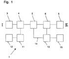
- the shown in Figure 1 in the form of a block diagram and circuit labeled 1 consists of an inductive element 2, for example a transformer, for the transmission of power and / or data in both directions, from an energy source 3 to an energy sink 5 and in the event of a change the potential relationships of that as an energy source effective energy sink 5 to the now as an energy sink effective energy source 3.
- an inductive element 2 for example a transformer
- converters 4 and 6 are connected, which are controlled in a special way.
- the converter 4 of the primary side I which also are connected to the energy source 3, by controls a switching signal source 11, which with a constant frequency is controlled.
- This frequency will generated by a clock generator 12, which is preferably contains a crystal oscillator.
- the Stromricher 6 of the secondary side II are through a control circuit 13 which is independent of the Switching signal source 11 assigned to power converters 4 works, controls.
- the control signals of the control circuit 13 become the inductive voltage curve Element 2 derived and from this via a Signal line 14 supplied to the control circuit 13.
- a quartz oscillator 15 assigned by which this runs stabilized. It must thus no longer every switching operation of the voltage the primary side I are used for synchronization, rather, the synchronization between the switching signal source 11 of the primary side I and the control circuit 13 the secondary side II, for example only for each hundredth switchover.
- the converters 4 of the primary side I are controlled by means of the switching signal source 11 with a stable and time-constant clock pattern.
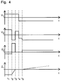
- the converters 4 are reversed each time the time period T z has elapsed, that is to say the voltage is reversed.
- the course of the voltage U 1 on the primary side I of the inductive element 2 thus results.
- the control is accomplished in such a way that, with a known cycle time T z, the converters 6 of the secondary side II are switched off a certain time beforehand. This is shown by the course of the release signal F after the waiting time T w (with T w ⁇ T z ).
- the converters 6 have a certain delay time Tigbt. Therefore, the secondary voltage does not change initially. After the delay time Tigbt has elapsed, the converters 6 block and the current is commented out, ie it goes to zero. As long as the current is commented out, the sign of the voltage U 2 changes . As soon as the current has become zero, the profile of the voltage U 2 is equal to that of the voltage U 1 , since the inductive element 2 is currentless. From this point in time, the change in voltage U 1 can be detected on secondary side II. As soon as the voltage U 1 and thus also the voltage U 2 is switched on by the converters 4 on the primary side I, the release signal F for the waiting time T w is released on the secondary side II and thus also the converters 6 on the secondary side II.
- the enable signal F is generated in such a way that interference can have no influence.
- a further fade-out time T s is waited until the commentary has ended, so that the course of the voltage U 2 can be reliably evaluated. This is illustrated in the time diagram according to FIG. 2 by the signal traffic jam.
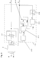
- a threshold signal 21 (Schmitt trigger) generates a switching signal S which does not reflect the level of the voltage U 2 but the level.
- the switching signal S is differentiated by means of a differentiator 22; the course of the signal S 'results.
- an auxiliary signal St is also generated via a logic element 23.
- the auxiliary signal St can only restart the timer 24 with the waiting time T w after an elapse of a timer 24 with the fade-out time T s via an auxiliary signal F 'and thus generate the release signal F.
- the auxiliary signal St is locked by the traffic jam signal when the enable signal F is withdrawn, which always takes place before the pulses of the signal S 'appear, since the converters 6 have a certain delay time.
Landscapes
- Engineering & Computer Science (AREA)
- Power Engineering (AREA)
- Dc-Dc Converters (AREA)
- Power Conversion In General (AREA)
- Rectifiers (AREA)
- General Induction Heating (AREA)
- Control Of Motors That Do Not Use Commutators (AREA)
Applications Claiming Priority (2)
| Application Number | Priority Date | Filing Date | Title |
|---|---|---|---|
| DE4202988A DE4202988A1 (de) | 1992-02-03 | 1992-02-03 | Verfahren zur ansteuerung von stromrichtern |
| DE4202988 | 1992-02-03 |
Publications (3)
| Publication Number | Publication Date |
|---|---|
| EP0554557A2 EP0554557A2 (de) | 1993-08-11 |
| EP0554557A3 EP0554557A3 (cg-RX-API-DMAC7.html) | 1994-03-23 |
| EP0554557B1 true EP0554557B1 (de) | 1998-03-18 |
Family
ID=6450839
Family Applications (1)
| Application Number | Title | Priority Date | Filing Date |
|---|---|---|---|
| EP92121649A Expired - Lifetime EP0554557B1 (de) | 1992-02-03 | 1992-12-19 | Verfahren zur Ansteuerung von Stromrichtern |
Country Status (5)
| Country | Link |
|---|---|
| EP (1) | EP0554557B1 (cg-RX-API-DMAC7.html) |
| JP (1) | JPH06133546A (cg-RX-API-DMAC7.html) |
| AT (1) | ATE164271T1 (cg-RX-API-DMAC7.html) |
| CA (1) | CA2088635A1 (cg-RX-API-DMAC7.html) |
| DE (2) | DE4202988A1 (cg-RX-API-DMAC7.html) |
Family Cites Families (2)
| Publication number | Priority date | Publication date | Assignee | Title |
|---|---|---|---|---|
| JP2773195B2 (ja) * | 1988-04-05 | 1998-07-09 | 松下電器産業株式会社 | スイッチング電源装置 |
| FR2645982B1 (fr) * | 1989-04-14 | 1991-06-14 | Alcatel Espace | Dispositif de regulation d'un parametre electrique lors d'un transfert d'energie entre deux reseaux |
-
1992
- 1992-02-03 DE DE4202988A patent/DE4202988A1/de not_active Withdrawn
- 1992-12-19 DE DE59209241T patent/DE59209241D1/de not_active Expired - Fee Related
- 1992-12-19 AT AT92121649T patent/ATE164271T1/de not_active IP Right Cessation
- 1992-12-19 EP EP92121649A patent/EP0554557B1/de not_active Expired - Lifetime
-
1993
- 1993-01-25 JP JP5010193A patent/JPH06133546A/ja active Pending
- 1993-02-02 CA CA002088635A patent/CA2088635A1/en not_active Abandoned
Non-Patent Citations (1)
| Title |
|---|
| etz-Archiv Bd. 12 (1990) H.8 Seiten 259-264 A.E$er, Th. Kalker:Berührungslose Energieversorgung dezentral angeordneter Antriebe in Handhabungsgeräten * |
Also Published As
| Publication number | Publication date |
|---|---|
| CA2088635A1 (en) | 1993-08-04 |
| EP0554557A2 (de) | 1993-08-11 |
| ATE164271T1 (de) | 1998-04-15 |
| DE59209241D1 (de) | 1998-04-23 |
| EP0554557A3 (cg-RX-API-DMAC7.html) | 1994-03-23 |
| DE4202988A1 (de) | 1993-08-05 |
| JPH06133546A (ja) | 1994-05-13 |
Similar Documents
| Publication | Publication Date | Title |
|---|---|---|
| DE69506096T2 (de) | Sperrwandler | |
| DE69103918T2 (de) | Synchronschaltsystem verwendender Leistungswandler mit hohem Wirkungsgrad. | |
| DE69119848T2 (de) | Festfrequenter Einrichtungsdurchlassumformer mit Nullspannungsschaltung | |
| DE60205002T2 (de) | Gleichstromrichter-Schaltnetzteil | |
| DE3031897C2 (cg-RX-API-DMAC7.html) | ||
| DE10251148A1 (de) | Nachreglernetzteil | |
| DE19709767C1 (de) | Verfahren zum Ansteuern mehrerer Schaltendstufen, Ansteuereinrichtung und Leistungsverstärker | |
| EP0698959B1 (de) | Sperrwandlerschaltung | |
| EP0978221A1 (de) | Schaltungsanordnung zum dimmbaren betrieb einer leuchtstofflampe | |
| DE69510903T2 (de) | Leistungsbegrenzender Regler | |
| EP0554557B1 (de) | Verfahren zur Ansteuerung von Stromrichtern | |
| DE602004001355T2 (de) | Anordnung mit einem Mikroprozessor, einer Entmagnetisierungsschaltung und einem Schaltnetzteil und einer zugehörigen Anzeigeeinheit | |
| EP0324089A2 (de) | Verfahren zum Erzeugen von Spannungsimpulsen | |
| DE69009256T2 (de) | Hochfrequenz-Hochspannungsleistungsversorgung mit Ausgangsleistungssteuerung. | |
| EP0214257A1 (de) | Ablenk-netzteil-konzept für fernsehgeräte | |
| DE3302756C2 (de) | Fernsehwiedergabeanordnung | |
| DE3025035C2 (de) | Verfahren und Anordnung zum unabhängigen Betreiben mehrerer elektrischer Triebfahrzeuge einer Modell- und Spielzeugeisenbahnanlage | |
| DE69732094T2 (de) | Transformatorgekoppelter schaltsender für elektronisches warenüberwachungssystem | |
| DE29800037U1 (de) | Vorrichtung zum Überwachen einer entlang eines vorgegebenen Weges bewegbaren Einrichtung sowie Modulatoreinheit und Auswerteeinheit für diese Vorrichtung | |
| DE19801499C2 (de) | Getaktete Stromversorgung | |
| DE60009222T2 (de) | Regelvorrichtung einer leuchtstofflampe | |
| DE69615345T2 (de) | Treiberschaltung für einen verschluss mit einem ferroelektrischen flüssigkristall | |
| WO2004036749A1 (de) | Verfahren und vorrichtung zur erzeugnung von zwei- oder mehrkanaligen pulsweitenmodulierten rechteckpulsen | |
| EP1364737A1 (de) | Stromquelle für ein Lichtbogenschweisssystem | |
| DE1763267C (de) | Verfahren zum Betrieb eines Generators zur Erzeugung von Steuersignalen für einen Wechselrichter und Generator zur Durchführung dieses Verfahrens |
Legal Events
| Date | Code | Title | Description |
|---|---|---|---|
| PUAI | Public reference made under article 153(3) epc to a published international application that has entered the european phase |
Free format text: ORIGINAL CODE: 0009012 |
|
| AK | Designated contracting states |
Kind code of ref document: A2 Designated state(s): AT BE CH DE ES FR GB IT LI NL PT SE |
|
| PUAL | Search report despatched |
Free format text: ORIGINAL CODE: 0009013 |
|
| AK | Designated contracting states |
Kind code of ref document: A3 Designated state(s): AT BE CH DE ES FR GB IT LI NL PT SE |
|
| 17P | Request for examination filed |
Effective date: 19940909 |
|
| 17Q | First examination report despatched |
Effective date: 19941230 |
|
| GRAG | Despatch of communication of intention to grant |
Free format text: ORIGINAL CODE: EPIDOS AGRA |
|
| GRAG | Despatch of communication of intention to grant |
Free format text: ORIGINAL CODE: EPIDOS AGRA |
|
| GRAH | Despatch of communication of intention to grant a patent |
Free format text: ORIGINAL CODE: EPIDOS IGRA |
|
| GRAH | Despatch of communication of intention to grant a patent |
Free format text: ORIGINAL CODE: EPIDOS IGRA |
|
| GRAA | (expected) grant |
Free format text: ORIGINAL CODE: 0009210 |
|
| AK | Designated contracting states |
Kind code of ref document: B1 Designated state(s): AT BE CH DE ES FR GB IT LI NL PT SE |
|
| PG25 | Lapsed in a contracting state [announced via postgrant information from national office to epo] |
Ref country code: ES Free format text: THE PATENT HAS BEEN ANNULLED BY A DECISION OF A NATIONAL AUTHORITY Effective date: 19980318 |
|
| REF | Corresponds to: |
Ref document number: 164271 Country of ref document: AT Date of ref document: 19980415 Kind code of ref document: T |
|
| REG | Reference to a national code |
Ref country code: CH Ref legal event code: EP |
|
| REF | Corresponds to: |
Ref document number: 59209241 Country of ref document: DE Date of ref document: 19980423 |
|
| GBT | Gb: translation of ep patent filed (gb section 77(6)(a)/1977) |
Effective date: 19980407 |
|
| ITF | It: translation for a ep patent filed | ||
| PG25 | Lapsed in a contracting state [announced via postgrant information from national office to epo] |
Ref country code: SE Free format text: LAPSE BECAUSE OF FAILURE TO SUBMIT A TRANSLATION OF THE DESCRIPTION OR TO PAY THE FEE WITHIN THE PRESCRIBED TIME-LIMIT Effective date: 19980618 Ref country code: PT Free format text: LAPSE BECAUSE OF FAILURE TO SUBMIT A TRANSLATION OF THE DESCRIPTION OR TO PAY THE FEE WITHIN THE PRESCRIBED TIME-LIMIT Effective date: 19980618 |
|
| ET | Fr: translation filed | ||
| PG25 | Lapsed in a contracting state [announced via postgrant information from national office to epo] |
Ref country code: AT Free format text: LAPSE BECAUSE OF NON-PAYMENT OF DUE FEES Effective date: 19981219 |
|
| PG25 | Lapsed in a contracting state [announced via postgrant information from national office to epo] |
Ref country code: BE Free format text: LAPSE BECAUSE OF NON-PAYMENT OF DUE FEES Effective date: 19981231 |
|
| PLBE | No opposition filed within time limit |
Free format text: ORIGINAL CODE: 0009261 |
|
| STAA | Information on the status of an ep patent application or granted ep patent |
Free format text: STATUS: NO OPPOSITION FILED WITHIN TIME LIMIT |
|
| 26N | No opposition filed | ||
| BERE | Be: lapsed |
Owner name: SCHWAN ULRICH Effective date: 19981231 |
|
| PGFP | Annual fee paid to national office [announced via postgrant information from national office to epo] |
Ref country code: NL Payment date: 20011220 Year of fee payment: 10 |
|
| REG | Reference to a national code |
Ref country code: GB Ref legal event code: IF02 |
|
| PGFP | Annual fee paid to national office [announced via postgrant information from national office to epo] |
Ref country code: DE Payment date: 20030618 Year of fee payment: 11 |
|
| PGFP | Annual fee paid to national office [announced via postgrant information from national office to epo] |
Ref country code: GB Payment date: 20030619 Year of fee payment: 11 |
|
| PGFP | Annual fee paid to national office [announced via postgrant information from national office to epo] |
Ref country code: CH Payment date: 20030620 Year of fee payment: 11 |
|
| PGFP | Annual fee paid to national office [announced via postgrant information from national office to epo] |
Ref country code: FR Payment date: 20030625 Year of fee payment: 11 |
|
| PG25 | Lapsed in a contracting state [announced via postgrant information from national office to epo] |
Ref country code: NL Free format text: LAPSE BECAUSE OF NON-PAYMENT OF DUE FEES Effective date: 20030701 |
|
| NLV4 | Nl: lapsed or anulled due to non-payment of the annual fee |
Effective date: 20030701 |
|
| PG25 | Lapsed in a contracting state [announced via postgrant information from national office to epo] |
Ref country code: GB Free format text: LAPSE BECAUSE OF NON-PAYMENT OF DUE FEES Effective date: 20031219 |
|
| PG25 | Lapsed in a contracting state [announced via postgrant information from national office to epo] |
Ref country code: LI Free format text: LAPSE BECAUSE OF NON-PAYMENT OF DUE FEES Effective date: 20031231 Ref country code: CH Free format text: LAPSE BECAUSE OF NON-PAYMENT OF DUE FEES Effective date: 20031231 |
|
| PG25 | Lapsed in a contracting state [announced via postgrant information from national office to epo] |
Ref country code: DE Free format text: LAPSE BECAUSE OF NON-PAYMENT OF DUE FEES Effective date: 20040701 |
|
| GBPC | Gb: european patent ceased through non-payment of renewal fee |
Effective date: 20031219 |
|
| REG | Reference to a national code |
Ref country code: CH Ref legal event code: PL |
|
| PG25 | Lapsed in a contracting state [announced via postgrant information from national office to epo] |
Ref country code: FR Free format text: LAPSE BECAUSE OF NON-PAYMENT OF DUE FEES Effective date: 20040831 |
|
| REG | Reference to a national code |
Ref country code: FR Ref legal event code: ST |
|
| PG25 | Lapsed in a contracting state [announced via postgrant information from national office to epo] |
Ref country code: IT Free format text: LAPSE BECAUSE OF NON-PAYMENT OF DUE FEES Effective date: 20051219 |