EP0550068A2 - Bildabtastgerät das Eichungssequenzen benutzt, die in verlängerten Teilen von Schieberegistern gespeichert sind - Google Patents
Bildabtastgerät das Eichungssequenzen benutzt, die in verlängerten Teilen von Schieberegistern gespeichert sind Download PDFInfo
- Publication number
- EP0550068A2 EP0550068A2 EP92122147A EP92122147A EP0550068A2 EP 0550068 A2 EP0550068 A2 EP 0550068A2 EP 92122147 A EP92122147 A EP 92122147A EP 92122147 A EP92122147 A EP 92122147A EP 0550068 A2 EP0550068 A2 EP 0550068A2
- Authority
- EP
- European Patent Office
- Prior art keywords
- shift registers
- image signals
- calibration
- stages
- array
- Prior art date
- Legal status (The legal status is an assumption and is not a legal conclusion. Google has not performed a legal analysis and makes no representation as to the accuracy of the status listed.)
- Granted
Links
Images


Classifications
-
- H—ELECTRICITY
- H04—ELECTRIC COMMUNICATION TECHNIQUE
- H04N—PICTORIAL COMMUNICATION, e.g. TELEVISION
- H04N25/00—Circuitry of solid-state image sensors [SSIS]; Control thereof
- H04N25/60—Noise processing, e.g. detecting, correcting, reducing or removing noise
- H04N25/67—Noise processing, e.g. detecting, correcting, reducing or removing noise applied to fixed-pattern noise, e.g. non-uniformity of response
- H04N25/671—Noise processing, e.g. detecting, correcting, reducing or removing noise applied to fixed-pattern noise, e.g. non-uniformity of response for non-uniformity detection or correction
- H04N25/672—Noise processing, e.g. detecting, correcting, reducing or removing noise applied to fixed-pattern noise, e.g. non-uniformity of response for non-uniformity detection or correction between adjacent sensors or output registers for reading a single image
-
- H—ELECTRICITY
- H04—ELECTRIC COMMUNICATION TECHNIQUE
- H04N—PICTORIAL COMMUNICATION, e.g. TELEVISION
- H04N25/00—Circuitry of solid-state image sensors [SSIS]; Control thereof
- H04N25/60—Noise processing, e.g. detecting, correcting, reducing or removing noise
- H04N25/67—Noise processing, e.g. detecting, correcting, reducing or removing noise applied to fixed-pattern noise, e.g. non-uniformity of response
- H04N25/671—Noise processing, e.g. detecting, correcting, reducing or removing noise applied to fixed-pattern noise, e.g. non-uniformity of response for non-uniformity detection or correction
- H04N25/673—Noise processing, e.g. detecting, correcting, reducing or removing noise applied to fixed-pattern noise, e.g. non-uniformity of response for non-uniformity detection or correction by using reference sources
-
- H—ELECTRICITY
- H04—ELECTRIC COMMUNICATION TECHNIQUE
- H04N—PICTORIAL COMMUNICATION, e.g. TELEVISION
- H04N25/00—Circuitry of solid-state image sensors [SSIS]; Control thereof
- H04N25/70—SSIS architectures; Circuits associated therewith
- H04N25/701—Line sensors
Definitions
- the present invention relates generally to image sensing apparatus, and more specifically to a technique for cancelling an amplitude difference between signals shifted along respective shift registers of an image sensor.
- the present invention is useful for application to facsimile machines and earth observation satellites.
- Multi-element image sensing apparatus used in applications such as facsimile and earth surveillance include a calibration system for periodically checking the functions of the apparatus in addition to circuitry for sensing images.
- a video signal is generated when the object of interest has a sufficient level of luminance for viewing, and a calibration is performed at other times.
- the image sensing apparatus comprises a linear array of image sensing elements and two shift registers one of which is connected to the odd-numbered elements of the array and the other is connected to the even-numbered elements of the array. Due to manufacturing tolerances, the operating characteristics of the shift registers are not necessary the same.
- a calibration pulse sequence of known amplitude is shifted along the shift registers and the sequences delivered from the shift registers are matched against each other to detect an amplitude difference.
- calibration is effected on the image signals subsequently output from the shift registers.
- an image sensing apparatus which comprises an array of image sensing elements, a first shift register having a plurality of stages divided into first and second sections, the stages of the first section corresponding respectively to odd-numbered elements of the array, and a second shift register having a plurality of stages divided into first and second sections, the stages of the first section corresponding respectively to even-numbered elements of the array.
- a transfer command pulse which is generated during each line scan interval
- gates are turned on and image signals developed in the odd-numbered elements of the array are transferred to the corresponding stages of the first shift register and image signals developed in the even-numbered elements of the array are transferred to the corresponding stages of the second shift register.
- a calibration sequence is generated and stored into the second section of each shift register when the gates are in a turn-off state, and the first and second shift registers are alternately driven to deliver the image signals and the calibration sequences therefrom.
- the image signals delivered from the first and second shift registers are combined to produce a complete video line signal.
- the difference in amplitude between the calibration sequences delivered from the first and second shift registers is detected, and the amplitude of the delivered image signals is controlled in response to the detected difference.
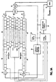
- the image sensor comprises a shift register 3 which is divided equally into a forward section 3A and a backward section 3B, and a shift register 5 which is likewise divided into a forward section 5A and a backward section 5B.
- a charge-coupled device 1 is provided having a linear array of 4,096 elements. The odd-numbered elements of the CCD are coupled via a transfer gate 2 to the forward section 3A of shift register 3, and the even-numbered elements of the CCD are coupled via a transfer gate 4 to the forward section 5A of shift register 5.
- shift register 3 The output end of shift register 3 is connected through an amplifier 6 to one input of a subtractor 7, and the output end of shift register 5 is connected through an amplifier 8 to one input of a subtractor 9.
- the outputs of subtractors 7 and 9 are combined by a multiplexer 10 and applied to an analog-to-digital converter 11
- the output of A/D converter 11 is connected to gates 12 and 13.
- the output of gate 12 is a digital video signal which is applied to a multiplexer 14 where it is multiplexed with a header and a trailer from a header/trailer generator 22 to produce a frame sequence for coupling to a transmitter, not shown, for where the signal is modulated upon a down-link carrier and transmitted toward an earth station.
- the output of gate 13 is a digital calibration sequence which is written into a read/write memory 15 in a location specified by a write address signal supplied from a read/write address generator 21. The stored calibration sequence is read out of memory 15 into one of latches 16 and 17 in response to a read address signal from the address generator 21.
- the outputs of latches 16 and 17 are connected to a digital comparator 18 where a difference is detected between the calibration sequences which have been shifted along shift registers 3 and 5, respectively.
- the difference value is converted into analog form by a digital-to-analog converter 19 and supplied to the subtractor 7 via a diode 28.
- An inverter 20 is connected to the output of D/A converter 19 to supply an inverted D/A converter output via a diode 29 to the subtractor 9.
- a timing controller 23 is connected to a clock source 24 to supply various timing signals to gates 2, 4, 12, 13, header/trailer generator 22, latches 16, 17 and address generator 21.
- a calibration sequence generator 25 is responsive to the clock pulse from clock source 24 for generating a sequence of pulses of prescribed amplitude.
- the calibration sequence is applied through gates 26 and 27 to the input ends of shift registers 3 and 5 when the gates 26, 27 are enabled by a control pulse from the timing controller 23.
- the calibration sequence is shifted along the respective shift registers when they are driven at a high clock rate and stored in the backward sections 3B and 5B of the shift registers.
- the transmitted signal is received by a demodulator of the earth station where the baseband video signal is recovered and applied to a clock recovery circuit 30 and a demultiplexer 31 where the signal is demultiplexed into a header and a trailer for coupling to a header/trailer detector 32, and a video signal for coupling to a D/A converter 33.
- the output of D/A converter 33 is applied to the image reproduction element of a scanner, not shown.
- the detected header and trailer are fed into a timing circuit 34 to produce a scanner control signal with which the scanner is driven to produce a raster image in a known manner.
- Calibration enable pulses are periodically supplied to gates 26 and 27 from the timing controller 23 to apply a calibration sequence of equal pulse amplitudes to the input ends of the shift registers 3, 5.
- the shift registers 3, 5 are clocked at a high rate so that all pulses of the calibration sequence are stored in a short period of time into their backward sections 3B, 5B.
- a transfer command pulse is generated by the timing controller 38 immediately following each calibration enable pulse and supplied to transfer gates 2 and 4.
- analog image signals developed in the odd-numbered elements of CCD 1 are transferred to the shift-register forward section 3A and those developed in the even-numbered elements of the CCD are transferred to the shift-register forward section 5A.
- the timing controller 23 supplies clock pulses alternately to the shift registers 3, 5 to shift the image signals as well as calibration sequences along stages to their output ends at a specified rate which is lower than the rate at which the calibration sequences have been stored. In this way, a first calibration sequence appears at the output end of shift register 3 following a sequence of odd-numbered image signals and a second calibration sequence appears at the output end of shift register 5 following a sequence of even-numbered image signals.
- the amplitudes of their calibration sequences are uniformly affected, or modulated accordingly as they are shifted along the shift register stages and assume different amplitude levels as they appear at the outputs of the shift registers, producing a amplitude difference D as shown in Fig. 2B.
- the outputs of shift registers 3, 5 are applied to subtractors 7 and 9 where the amplitudes of the image signals are increased or decreased by an amount determined by the polarity and magnitude of a difference detected by the comparator 18 between odd- and even-numbered calibration sequences of a previous line scan.
- a multiplexed output sequence of image signals and a multiplexed output sequence of amplitude-modulated calibration pulses are supplied from multiplexer 10 to A/D converter 11 and digital versions of the video line signal and calibration sequence are generated.
- the timing controller 23 enables the gate 12 to apply the digital video signal to multiplexer 14 where it is combined with a header and a trailer for transmission, and then enables the gate 13 to store the digital calibration sequence into memory 15 while at the same time causing the address generator 21 to supply a write address signal to memory 15.
- the timing controller 23 directs the address generator 21 to supply a read address signal to memory 15 and at the same time alternately enables the latches 16 and 17 to separately latch the odd- and even-numbered components of the amplitude-modulated calibration sequence.
- Digital comparator 18 makes a comparison between the amplitudes of the latched odd- and even-numbered components and generates a digital differential signal, which is converted to analog form by D/A converter 19 for coupling to one of subtractors 7 and 9 depending on the polarity of the differential signal.
- the differential signal represents the difference between the operating characteristics of shift registers 3 and 5 and the amplitudes of the image signals from the odd- or even-numbered elements of the CCD 1 are varied to compensate for the difference in characteristics.
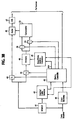
- FIGs. 3A and 3B An alternative embodiment of the present invention is shown in Figs. 3A and 3B.
- This embodiment differs from the previous embodiment in that the circuitry that utilizes the modulated calibration sequence for error compensation is provided in the receiving earth station in order to simplify the transmitter's circuitry. Therefore, the outputs of amplifiers 6 and 8 are directly combined by multiplexer 10 and fed to A/D converter 11, and the output of A/D converter 11, including both video and calibration sequences, is directly coupled to multiplexer 14 and multiplexed with a header and a trailer for transmission.
- Fig. 3B on receiving a signal from the transmitter, it is demodulated by the receiving station to recover the baseband signal, which is supplied to a clock recovery circuit 40 and demultiplexer 41 where the signal is demultiplexed into a header/trailer portion for coupling to a header/trailer detector 42 and a video and calibration signal portion for coupling to gates 44 and 45.
- the outputs of header/trailer detector 42 and the clock recovery circuit 40 are applied to a timing controller 43 to generate various timing signals.
- Gate 44 is initially enabled by the timing controller to pass the digital video sequence to an adder 46 whose output is connected to a D/A converter 47.
- Gate 45 is subsequently enabled to pass the digital calibration sequence to a memory 48 to which a write address signal is also supplied from a read/write address generator 49.
- the latter derives the address signal from a read/write enable signal from timing controller 43 and a clock pulse from the clock recovery circuit 40.
- Latches 50 and 51 are connected to the output of memory 48, and a digital comparator 52 is provided for making a comparison between the outputs of the latches and supplies a digital differential signal to the adder 46.
- the timing controller 43 applies a read enable signal to address generator 49 while alternately enabling the latches 50 and 51 to respectively latch the odd- and even-numbered calibration components.
- Comparator 52 detects the difference between these components and provides a digital compensation signal to adder 46 to increase or decrease the amplitude of the incoming digital video signal in accordance with the digital compensation signal.
- the compensated video signal is converted to analog form by D/A converter 47 and applied to a scanner, not shown.
Landscapes
- Engineering & Computer Science (AREA)
- Multimedia (AREA)
- Signal Processing (AREA)
- Transforming Light Signals Into Electric Signals (AREA)
- Solid State Image Pick-Up Elements (AREA)
- Facsimile Heads (AREA)
Applications Claiming Priority (3)
| Application Number | Priority Date | Filing Date | Title |
|---|---|---|---|
| JP360351/91 | 1991-12-30 | ||
| JP3360351A JP2725508B2 (ja) | 1991-12-30 | 1991-12-30 | 多素子光センサ装置 |
| JP36035191 | 1991-12-30 |
Publications (3)
| Publication Number | Publication Date |
|---|---|
| EP0550068A2 true EP0550068A2 (de) | 1993-07-07 |
| EP0550068A3 EP0550068A3 (de) | 1993-08-04 |
| EP0550068B1 EP0550068B1 (de) | 2001-05-30 |
Family
ID=18469030
Family Applications (1)
| Application Number | Title | Priority Date | Filing Date |
|---|---|---|---|
| EP92122147A Expired - Lifetime EP0550068B1 (de) | 1991-12-30 | 1992-12-30 | Bildabtastgerät das Eichungssequenzen benutzt, die in verlängerten Teilen von Schieberegistern gespeichert sind |
Country Status (4)
| Country | Link |
|---|---|
| US (1) | US5317423A (de) |
| EP (1) | EP0550068B1 (de) |
| JP (1) | JP2725508B2 (de) |
| DE (1) | DE69231848T2 (de) |
Cited By (1)
| Publication number | Priority date | Publication date | Assignee | Title |
|---|---|---|---|---|
| WO2002052233A3 (en) * | 2000-12-26 | 2002-12-19 | Honeywell Int Inc | Lightweight infrared camera |
Families Citing this family (6)
| Publication number | Priority date | Publication date | Assignee | Title |
|---|---|---|---|---|
| JP2770795B2 (ja) * | 1995-07-19 | 1998-07-02 | 日本電気株式会社 | 多素子センサの校正方法及びその装置 |
| JPH1084279A (ja) * | 1996-09-06 | 1998-03-31 | Sony Corp | Pll回路およびこれを用いた記録再生装置 |
| JP3000979B2 (ja) | 1997-11-11 | 2000-01-17 | 日本電気株式会社 | 多素子センサの校正装置 |
| JP3766192B2 (ja) * | 1997-11-13 | 2006-04-12 | 株式会社東芝 | 光電変換装置、光電変換方法、画像情報処理装置、画像情報処理方法、および画像形成装置 |
| JP3899627B2 (ja) * | 1998-01-06 | 2007-03-28 | 富士ゼロックス株式会社 | リニアイメージセンサおよび画像読み取り装置および電荷転送方法 |
| US8501561B2 (en) | 2006-03-07 | 2013-08-06 | Infineon Technologies Ag | Method for producing a semiconductor component arrangement comprising a trench transistor |
Family Cites Families (9)
| Publication number | Priority date | Publication date | Assignee | Title |
|---|---|---|---|---|
| US4216503A (en) * | 1979-03-26 | 1980-08-05 | Xerox Corporation | Signal restoration and gain control for image viewing devices |
| JPS6028183B2 (ja) * | 1980-11-28 | 1985-07-03 | 松下電送株式会社 | 画像読取装置 |
| US4712137A (en) * | 1981-07-20 | 1987-12-08 | Xerox Corporation | High density CCD imager |
| US4555732A (en) * | 1984-03-22 | 1985-11-26 | Xerox Corporation | Image sensor correction system |
| US4665440A (en) * | 1985-09-17 | 1987-05-12 | Honeywell, Inc. | Parallel processing of the output from monolithic sensor arrays |
| JPH01305672A (ja) * | 1988-06-02 | 1989-12-08 | Nec Corp | 電荷結合素子の信号処理装置 |
| JPH0693768B2 (ja) * | 1988-12-27 | 1994-11-16 | 日本電気株式会社 | 撮像信号処理装置 |
| EP0473966B1 (de) * | 1990-08-09 | 1996-03-27 | Sony Corporation | CCD mit einem Paar von horizontalen Registern |
| US5204761A (en) * | 1991-03-18 | 1993-04-20 | Xerox Corporation | Pixel by pixel offset and gain correction in analog data from scanning arrays |
-
1991
- 1991-12-30 JP JP3360351A patent/JP2725508B2/ja not_active Expired - Lifetime
-
1992
- 1992-12-30 US US07/998,384 patent/US5317423A/en not_active Expired - Lifetime
- 1992-12-30 EP EP92122147A patent/EP0550068B1/de not_active Expired - Lifetime
- 1992-12-30 DE DE69231848T patent/DE69231848T2/de not_active Expired - Lifetime
Cited By (5)
| Publication number | Priority date | Publication date | Assignee | Title |
|---|---|---|---|---|
| WO2002052233A3 (en) * | 2000-12-26 | 2002-12-19 | Honeywell Int Inc | Lightweight infrared camera |
| US6559447B2 (en) | 2000-12-26 | 2003-05-06 | Honeywell International Inc. | Lightweight infrared camera |
| EP1767912A3 (de) * | 2000-12-26 | 2007-08-22 | Honeywell International, Inc. | Leichtbau-infrarotkamera |
| CN100414274C (zh) * | 2000-12-26 | 2008-08-27 | 霍尼韦尔国际公司 | 重量轻的红外照相机 |
| KR100876459B1 (ko) * | 2000-12-26 | 2008-12-31 | 허니웰 인터내셔널 인코포레이티드 | 경량 적외선 카메라 |
Also Published As
| Publication number | Publication date |
|---|---|
| EP0550068A3 (de) | 1993-08-04 |
| JP2725508B2 (ja) | 1998-03-11 |
| US5317423A (en) | 1994-05-31 |
| EP0550068B1 (de) | 2001-05-30 |
| JPH05183143A (ja) | 1993-07-23 |
| DE69231848D1 (de) | 2001-07-05 |
| DE69231848T2 (de) | 2001-10-04 |
Similar Documents
| Publication | Publication Date | Title |
|---|---|---|
| KR920003655B1 (ko) | 고속 셔터기능이 있는 고체 촬상소자와 고체 촬상소자에서 고속 셔터기능을 실현하는 방법 | |
| US5420631A (en) | Solid state image pickup device and method | |
| US8681253B2 (en) | Imaging system for creating an output signal including data double-sampled from an image sensor | |
| US4472744A (en) | Photoelectric converter apparatus | |
| JPH02291764A (ja) | 両面走査装置 | |
| EP0748112B1 (de) | Festkörper-Bildsensor und Ansteuerungsverfahren dazu | |
| US5317423A (en) | Image sensing apparatus using calibration sequences stored in extended portions of shift registers | |
| US6803952B1 (en) | Signal readout circuit of an amplification type solid-state imaging device | |
| JPH0522668A (ja) | 固体撮像装置 | |
| JPS6027870A (ja) | スタ−センサにおけるデ−タ処理装置 | |
| US6950132B1 (en) | Image sensor and method for driving an image sensor for reducing fixed pattern noise | |
| JPS63299581A (ja) | 画像撮像及び表示システム及びそのシステムに適する画像撮像装置 | |
| KR920005599A (ko) | 2개의 수평레지스터를 가진 고체촬상장치 | |
| US4939578A (en) | Method of driving multiple chip CCD image sensor | |
| US8593699B2 (en) | Image sensor module and image sensor | |
| US4663672A (en) | Image reading apparatus | |
| EP0223260B1 (de) | Signalleseschaltungsanordnung für maskierte und überlappende lineare Bildsensoren | |
| US4652927A (en) | Image sensing device | |
| TW200529659A (en) | Image sensor array with variable resolution and high-speed output | |
| JPH0746869B2 (ja) | 擬似動画伝送方法 | |
| US5613156A (en) | Imaging system with 1-N Parallel channels, each channel has a programmable amplifier and ADC with serial controller linking and controlling the amplifiers and ADCs | |
| JPH11234472A (ja) | 密着型イメージセンサとその駆動方法及び光電変換装置と画像読取装置 | |
| US5963338A (en) | Method and apparatus for calibrating multi-element sensors | |
| JPS6188682A (ja) | 画像処理回路 | |
| JPH09321953A (ja) | 撮像装置 |
Legal Events
| Date | Code | Title | Description |
|---|---|---|---|
| PUAI | Public reference made under article 153(3) epc to a published international application that has entered the european phase |
Free format text: ORIGINAL CODE: 0009012 |
|
| PUAL | Search report despatched |
Free format text: ORIGINAL CODE: 0009013 |
|
| AK | Designated contracting states |
Kind code of ref document: A2 Designated state(s): DE FR GB |
|
| AK | Designated contracting states |
Kind code of ref document: A3 Designated state(s): DE FR GB |
|
| 17P | Request for examination filed |
Effective date: 19930623 |
|
| 17Q | First examination report despatched |
Effective date: 19951204 |
|
| GRAG | Despatch of communication of intention to grant |
Free format text: ORIGINAL CODE: EPIDOS AGRA |
|
| GRAG | Despatch of communication of intention to grant |
Free format text: ORIGINAL CODE: EPIDOS AGRA |
|
| GRAG | Despatch of communication of intention to grant |
Free format text: ORIGINAL CODE: EPIDOS AGRA |
|
| GRAH | Despatch of communication of intention to grant a patent |
Free format text: ORIGINAL CODE: EPIDOS IGRA |
|
| GRAH | Despatch of communication of intention to grant a patent |
Free format text: ORIGINAL CODE: EPIDOS IGRA |
|
| GRAA | (expected) grant |
Free format text: ORIGINAL CODE: 0009210 |
|
| AK | Designated contracting states |
Kind code of ref document: B1 Designated state(s): DE FR GB |
|
| REF | Corresponds to: |
Ref document number: 69231848 Country of ref document: DE Date of ref document: 20010705 |
|
| ET | Fr: translation filed | ||
| REG | Reference to a national code |
Ref country code: GB Ref legal event code: IF02 |
|
| REG | Reference to a national code |
Ref country code: GB Ref legal event code: 732E |
|
| PLBE | No opposition filed within time limit |
Free format text: ORIGINAL CODE: 0009261 |
|
| STAA | Information on the status of an ep patent application or granted ep patent |
Free format text: STATUS: NO OPPOSITION FILED WITHIN TIME LIMIT |
|
| 26N | No opposition filed | ||
| REG | Reference to a national code |
Ref country code: FR Ref legal event code: TP |
|
| PGFP | Annual fee paid to national office [announced via postgrant information from national office to epo] |
Ref country code: GB Payment date: 20101229 Year of fee payment: 19 |
|
| PGFP | Annual fee paid to national office [announced via postgrant information from national office to epo] |
Ref country code: FR Payment date: 20111219 Year of fee payment: 20 |
|
| PGFP | Annual fee paid to national office [announced via postgrant information from national office to epo] |
Ref country code: DE Payment date: 20111229 Year of fee payment: 20 |
|
| REG | Reference to a national code |
Ref country code: DE Ref legal event code: R071 Ref document number: 69231848 Country of ref document: DE |
|
| REG | Reference to a national code |
Ref country code: GB Ref legal event code: PE20 Expiry date: 20121229 |
|
| PG25 | Lapsed in a contracting state [announced via postgrant information from national office to epo] |
Ref country code: GB Free format text: LAPSE BECAUSE OF EXPIRATION OF PROTECTION Effective date: 20121229 |
|
| PG25 | Lapsed in a contracting state [announced via postgrant information from national office to epo] |
Ref country code: DE Free format text: LAPSE BECAUSE OF EXPIRATION OF PROTECTION Effective date: 20130101 |