EP0544964B1 - Appareil à mémorisation et à transmission et méthode pour maintenir l'intégrité des données pendant leur stockage - Google Patents
Appareil à mémorisation et à transmission et méthode pour maintenir l'intégrité des données pendant leur stockage Download PDFInfo
- Publication number
- EP0544964B1 EP0544964B1 EP91480175A EP91480175A EP0544964B1 EP 0544964 B1 EP0544964 B1 EP 0544964B1 EP 91480175 A EP91480175 A EP 91480175A EP 91480175 A EP91480175 A EP 91480175A EP 0544964 B1 EP0544964 B1 EP 0544964B1
- Authority
- EP
- European Patent Office
- Prior art keywords
- fcs
- bit
- frame
- lead
- input
- Prior art date
- Legal status (The legal status is an assumption and is not a legal conclusion. Google has not performed a legal analysis and makes no representation as to the accuracy of the status listed.)
- Expired - Lifetime
Links
Images


Classifications
-
- H—ELECTRICITY
- H04—ELECTRIC COMMUNICATION TECHNIQUE
- H04L—TRANSMISSION OF DIGITAL INFORMATION, e.g. TELEGRAPHIC COMMUNICATION
- H04L12/00—Data switching networks
- H04L12/54—Store-and-forward switching systems
- H04L12/56—Packet switching systems
-
- H—ELECTRICITY
- H04—ELECTRIC COMMUNICATION TECHNIQUE
- H04L—TRANSMISSION OF DIGITAL INFORMATION, e.g. TELEGRAPHIC COMMUNICATION
- H04L1/00—Arrangements for detecting or preventing errors in the information received
- H04L1/0078—Avoidance of errors by organising the transmitted data in a format specifically designed to deal with errors, e.g. location
Definitions
- the invention relates to store and forward mechanisms for telecommunication equipments and particularly to an apparatus including means for deserializing a HDLC frame of data which is received from a first telecommunication node under the form of a sequence of n-bits words, the frame including a header, a data field and a frame checking sequence (FCS) generated by the first node.
- the apparatus includes a storage for storing the deserialized n-bit words thru Direct Memory Access means, processing means computing a new header for replacement of the header of the received HDLC frame in said storage.
- the store and forward apparatus comprises serializing means which fetches the n-bit words in the storage thru the DMA means and which forwards them under the form of a new HDLC frame including a new FCS, to a second telecommunication node.
- erroneous data might be introduced in the frame as the latter is transmitted from one node to another.
- Such errors are effectively detected by using well known Frame Checking Sequences (FCS) or CRC checksums involved in the High Data Link Control (HDLC) procedures.
- FCS Frame Checking Sequences
- HDLC High Data Link Control
- the transmitting station sends a packet and appends to it an appropriate computed CRC checksum.
- the receiving node stores the transmitted checksum, calculates its own one, and compares the two to detect the occurence of a possible error during the transmission throughout the line.
- the technical problem to be solved consists in the conception of a store and forward mechanism for a telecommunication machine running with a HDLC protocol, by which it is possible to assure the integrity of data during its transfer within the storage of the machine without requiring any processing resources from the processor therein included and further delay.
- the store and forward includes means receiving in parallel the received HDLC frame simultaneously to the deserializing means and which computes a first partial FCS over the data field, and means for storing that partial FCS.
- the n-bits words which are to be transmitted to the next telecommunication node are simultaneously received by the HDLC serializer and by means for computing a second partial FCS covering said data field only of said forwarded HDLC frame.
- the two partial results are compared in order to detect the occurence of an error which might have appeared in the storage during the computing of the new header of the frame.
- the result of that comparison is used as a control signal for altering the value of the FCS computed by the HDLC computed and before it is transmitted to the telecommunication line. Since the computing of both the first and second partial FCS is respectively performed during the deserializing of the HDLC frame and the serializing of the processed n-bit data words, no extra delay is required. The integrity of data during its storage in RAM is therefore provided without needed additional processing resources since the processor which is included within the store and forward mechanism has its resources which remain fully allocated for the store and forward process.
- the store and forward mechanism includes a FIFO storage which has an output bus which is separate from the data bus which addresses the RAM. In this way, the comparison of the first and second partial results do not require the access of the data bus.
- the deserializing means is a HDLC receiver which deserializes HDLC frames into n-bit words and which generates a control signal for setting a latching circuit when the first bit of the data field of the incoming frame is received, and a second control signal for resetting said latching circuit when the last bit of the data field of said HDLC frame has been received.
- the said means for computing said first partial FCS is a FCS generator which receives the serial frame at its input and which has a clock input being controlled by the output of said latching circuit. This allows the used of widely known FCS generators, and the partial FCS result is computed only by controlling the signal entered at its clock input.
- the serializing means is a HDLC transmitter which has a control input for causing an alteration of the next bit which will appear at its output, and the control input receives the result of the comparison of the first and second partial result.
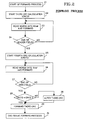
- Figure 1 is a basic flow chart detailing the principle of the storing process of the store and forward mechanism according to the present invention.
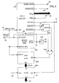
- Figure 2 is a basic flow chart detailing the principle of the forward process involved in the store and forward mechanism according to the present invention.
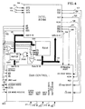
- Figures 3, 4 and 5 are an illustration of a preferred embodiment of a store and forward mechanism according to the present invention.
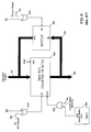
- FIG. 6 is an illustration of the Direct Memory Access (DMA) receive part of DMA control circuit 900.
- DMA Direct Memory Access
- Figure 7 is an illustration of the DMA transmit part of the DMA control circuit 900.
- Figure 8A and 9 illustrates the first and second internal DMA receive state machines which are included into circuit 900.
- Figure 8B shows typical timing diagrams of the bus access control signals.
- Figure 10A and 11 illustrate the first and second internal DMA transmit state machines which are included into DMA control circuit 900.
- Figure 10B shows typical timing diagrams of the bus access control signals.
- FIG. 1 shows the principle of the storing process according to the present invention.
- the apparatus is ready to receive HDLC or SDLC frames, step 10.
- the processing of one received frame begins on the detection of the traditional HDLC or SDLC flag, step 11.
- Step 12 the deserializer which is included into the receive part of the telecommunication node starts computing the Frame Checking Sequence (FCS) or CRC checksum on the first bit of the header field.
- FCS Frame Checking Sequence
- the received bits are sequentially grouped into n-bit words and are successively stored into the RAM as they appear at the output of the HDLC receiver until the last bit of the header field, which is detected by means of a test on the last bit of the header field, step 14.
- step 15 On the occurence of the last bit of the header field, the process goes to step 15 where a second CRC computing is initiated by a separate CRC generator parallely to the above first CRC computation.
- the deserialization process of the incoming frame then continues and the received bits are groups and stored into the storage, step 16, until the occurence of the last bit of the data field of the HDLC frame. That last bit is detected by means of a test which is performed in step 17.
- Step 18 the result of the second CRC calculation is stored into a FIFO storage as the result of the first one is used, as traditionally, to check the integrity of the HDLC frame received from the line.
- the forward process can start when the new header has been computed, step 21.
- step 22 the first n-bits word corresponding to the first bits of the header are provided to the serializer which immediately starts the computation of a CRC, hereinafter referred to as the third CRC computation, which will be transmitted to the next telecommunication node.
- the n-bit data words are successively read from the storage while the HDLC transmitters generates the corresponding memori of data bits which are forwarded to the network. This is achieved by means of a read/forward operation performed in step 23 in order to extracts the groups of bits from the storage and to send them to the HDLC transmitter, associated with a test in step 24 in order to detect the end of the header field of the HDLC frame to be transmitted.
- step 23 a new group of bits is read from the memory and provided at the input of the serializer.
- a fourth CRC computation process is started, step 25, in a second separate CRC generator having its input bus connected to the input of the HDLC transmitter.
- that second CRC computation is processed parallely to the CRC computation which is performed in the HDLC serializer and which started with the first bit of the header field of the HDLC frame to be transmitted.
- the serialization process of the HDLC frame then continues with the serialization of the data field of the frame.
- step 26 the following group of bits of the data field is extracted from the storage and provided to the HDLC serializer and also to the above second separate CRC generator.
- step 27 a test is performed to determine whether the current group of data which is serialized is the last group of the data field of the HDLC frame, in which case the process proceeds to step 29. In the reverse case, the process goes back to step 26 where the next group of data bits is extracted from the storage and serialized by the HDLC serializer.
- the fourth CRC computation process completes and its result is compared with the result of the second CRC computation which was stored into the FIFO.
- step 28 the apparatus will generate a alteration control signal which will indicate the HDLC serializer, which has also completed its own CRC checksum calculation but not yet transmitted on the line, to alter the latter result.
- the latter is then forward by the telecommunication line to the next telecommunication node in step 30. That next node will easily detect the error introduced during the storage of the bits into the RAM by means of the traditional FCS or CRC checksum computation which is traditionally performed in the receive part of that next node.
- the frame forward process completes, step 31.
- the second and fourth CRC computation process are performed on the serial train of bits, parallely to the deserialization and serialization process, no further processing delay is required in the whole processing of the received HDLC frame.
- the resources of the processor which is included into the telecommunication node providing the store and forward mechanism in accordance to the present invention still remain affected to the traditional processing of the header of the HDLC frame.
- Figures 3, 4 and 5 illustrate a preferred embodiment of the store and forward mechanism according to the invention.
- the mechanism comprises a microcontroller 100 such as the 16 bits INTEL 80186 which is connected to a RAM storage 200, being of the type 64 000 x 16 bits, by means of an address bus 131, a data bus 101 and traditional Chip Select (CS), write (WR) and read (RD) control leads.
- controller 100 is also connected to a traditional SDLC receiver 300, the latter being associated with a RECEIVE CLOCK generator 400, and a CRC2 generator 500.
- Controller 100 is further connected to a SDLC transmitter 600 which is associated to a TRANSMIT CLOCK generator 700 and a CRC2' generator 800 which are illustrated in figure 5.
- SDLC RECEIVER 300 has DATA END output lead 111 which is connected to a reset input of a latch 1030, and a DATA BEGIN output lead 112 which is connected to the set input lead of the latter latch.
- the Q output lead of latch 1030 is connected to one input lead of an AND gate 1040 which has an output connected to the clock input of CRC2 generator 500, and a second input lead receiving the RECEIVE clock generated at the bit clock output lead 113 of RECEIVE CLOCK GENERATOR 400.
- Generator 400 also generates a byte clock on a lead 115 which is transmitted to the input of a divide-by-two circuit 1020.
- Divide-by-two circuit 1020 has an output lead 116 which is connected to a CLOCK WORD RECEIVE input lead of DMA CONTROL circuit 900. Because of the division by two of the byte clock, the signal transmitted to the input 116 of DMA control circuit 900 is is phase with the bit clock generated on lead 113 but only consists in a clock pulse occuring on the appearance of a 16-bit word on 16-bit data bus 101.
- SDLC RECEIVE circuit 300 has respectively a HEADER END output lead 119 and a HEADER BEGIN output lead 120 which are connected to interrupt INTO input lead and INT1 input lead of controller 100. HEADER BEGIN signal on lead 120 is also transmitted to the HEADER BEGIN input lead of DMA CONTROL circuit 900.
- SDLC RECEIVE circuit 300 shares with controller 100, with RAM storage 200, with a buffer 1000, with DMA CONTROL circuit 900, with SDLC XMIT circuit 600, and with CRC2' generator 800 the same 16-bit data bus 101.
- SDLC RECEIVE circuit 300 has an CS RX receive input which is connected to a corresponding CS RX output of DMA CONTROL circuit 900 by means of a lead 118, a CRC1 END output which is connected to a INC input of a FIFO 2000 and to a CRC1 input of DMA CONTROL circuit 900 by means of a lead 117, and a CLOCK input which receives the BYTE clock on lead 115.
- RECEIVE CLOCK generator 400 generates the receive clock signal on lead 113 which is transmitted, for instance, to a Data Terminating Equipment and controls rythm of the reception of the incoming frame.
- CRC2 generator 500 generates, as described below, a 16-bit CRC2 pattern which is transmitted to a 16 bit input bus of FIFO 2000.
- the latter FIFO has an output 16-bit bus 121 which is connected to a first input bus of a comparator 2010 illustrated in figure 5, having a second input bus which is connected to a 16-bit output bus of CRC2' generator 800.
- Controller 100 has a CS5 output lead 127, a HLDA output lead 126, a HOLD input lead 125, a CS1 output lead 124, a CS2 output lead 123, a CS6 output lead 129, a CS4 output lead 128 which are respectively connected to a CS CRC2' BEGIN input lead, a HLDA input lead, a HOLD output, a CS ADDRESS COUNTER input lead, a CS END input lead, a CS RECEIVE COUNT input lead, and ENABLE FORWARD input lead of DMA CONTROL circuit 900.
- Controller 100 has a READ control signal which is transmitted to a RD input lead of DMA CONTROL circuit 900 and to a first input of an OR gate 3001.
- gate 3001 has a second input which receives the CS3 signal on lead 132, and has an output which is connected to a first input of an AND gate 3000.
- Controller 100 has a WR control signal which is transmitted to a first input of an OR gate 1050, and to a WR lead of DMA CONTROL 900.
- OR gate 1050 has a second input lead which is connected to CS3 output lead 132 of controller 100 and has an output lead which is connected to a second input of an AND gate 3000.
- AND gate 3000 has an output lead which is connected to the OUTPUT ENABLE input of a buffer 1060.
- DMA CONTROL circuit 900 has a LOAD XMIT output lead 212 which is connected to a corresponding LOAD input lead of SDLC XMIT circuit 600 and also to the LOAD input of CRC2' generator 800. Further, DMA CONTROL circuit 900 has a ENB CRC2' CALC output lead 214 which is connected to a first input lead of an AND gate 1070, and a XMIT FLAG END input lead 122 which is connected to a FLAG END output lead of SDLC Xmit circuit 600 and also to a DECrement input lead of FIFO 2000.
- AND 1070 has a second input lead which receives the transmit clock on lead 215 which is generated at the bit clock output lead of XMIT CLOCK generator 700. The latter clock is also provided to the CLOCK input of SDLC XMIT circuit 600.
- XMIT CLOCK generator 700 has a CLOCK WORD XMIT output lead 211 which is connected to a corresponding CLOCK WORD XMIT input lead of DMA CONTROL circuit 900.
- the output lead of AND gate 1070 is connected to the CLOCK input of CRC2' generator 800.
- Comparator 2010 has an output lead which is transmitted to a first input lead of an AND gate 1080, a second input of which being connected to the CRC BEGIN output lead of SDLC XMIT circuit 600.
- AND gate 1080 provides at its output lead a SPOIL CRC signal to SDLC XMIT circuit 600 which will be used as a control signal for altering the CRC checksum which is computed into SDLC TRANSMIT circuit 600.
- XMIT CLOCK generator 700 and SDLC XMIT circuit 600 respectively provides a XMIT clock and a XMIT data which are transmitted to the next telecommunication node.
- DMA CONTROL circuit 900 is particularly illustrated with respect to figures 6 and 7 which respectively details the receive and the transmit parts.
- DMA CONTROL circuit 900 has a DMA RECEIVE COUNTER 920 which is connected to 16-bit data bus 101 and which has a 16-bit output bus 901 which is connected to a corresponding input bus of a tri-state buffer 910.
- Buffer 910 has its output bus which is connected to bus 901 and is controlled by an OR gate 930, the output of which being connected to the OUTPUT ENABLE input lead of buffer 910.
- OR gate 930 has its two input leads which respectively receives RD control signal and CS RECEIVE COUNT control signal on lead 129 coming from controller 100.
- DMA RECEIVE COUNTER 920 has a Load (LD) input lead which is connected to the output of an OR 940 receiving WR control signal and CS RECEIVE COUNT signal on lead 129 at its two inputs.
- An AND gate 950 receives a ENABLE CLOCK WORD RECEIVE signal from an internal state machine 960 at ist first input lead.
- gate 950 has its second input which receives CLOCK WORD signal on lead 116 and which is generated by divide-by-two circuit 1020.
- DMA RECEIVE COUNTER 920 has a POR reset input lead which receives the general power-on of the telecommunication equipment.
- FIG. 7 illustrates the internal circuitry corresponding to the transmit part of DMA CONTROL circuit 900.
- a 16-bit DMA XMIT COUNTER 961 has an input bus which is connected to the 16-bit data bus 101, and a 16 bit output bus 911 which is connected to an input bus of a buffer 962, to a first input bus of a first comparator 963 and to a first input bus of a second comparator 964.
- Comparator 963 has a second input bus which is connected to the output bus of latching circuit 966 and a output lead which is connected to a set input of a latch 967.
- Latch 967 has its reset lead which receives the XMIT FLAG END signal on lead 122, and an output lead which provides the ENABLE CRC2' CALC signal on lead 214.
- Latching circuit 966 has its input bus which is connected to data bus 101 and has an ENABLE input lead which receives the CS CRC2' BEGIN signal on lead 127 which is generated by microcontroller 100.
- Comparating circuit 964 has its second input bus which is connected to the output of a latching circuit 965 and has an output lead which is connected to a STOP COUNT input lead of counter 961 and which is used for stopping the incrementation of the latter.
- Latching circuit 965 receives at its input the contents of data bus 101 and has a ENABLE input lead which receives the CS END signal on lead 123 generated by controller 100.
- Buffer 962 has an OUTPUT ENABLE lead which receives the output of an OR gate 968, the two input of which receiving the RD control signal and the CS ADDRESS COUNTER signal on lead 124 and generated by controller 100.
- Counter 961 has a CLOCK input lead which is connected to the output of an AND gate 969 having a first input lead receiving CLOCK WORD XMIT signal 211 which is generated by XMIT CLOCK generator 700.
- AND gate 969 has a second input lead which receives an ENABLE CLOCK WORD XMIT signal provided by an internal state machine 972 which will be described later on with respect to figure 11.
- Counter 961 has a LOAD input lead which receives the output of an OR gate 971 having its two input which respectively receives the write (WR) control signal and the CS ADDRESS COUNTER signal 124 which is generated by controller 100.
- the invention operates as follows. At the power-on of the machine, an initialization process begins during which, particularly, the contents of DMA RECEIVE COUNTER 920 and DMA XMIT COUNTER 961 are reset. Then, during the actual data transmission process, frames are received by SDLC RECEIVER 300, for instance coming from a Data Terminating equipment.
- the incoming frames are well known SDLC frames consisting in the succession of the SDLC flag ('7E' in hexadecimal), followed by a header, the data to be transmitted, a 16-bit CRC checksum and, at last, a SDLC flag.
- the incoming frame is received at the RECEIVE DATA input lead 114 of SDLC RECEIVE circuit 300 which performs the traditional zero delete and deserialization of the frame.
- SDLC RECEIVE circuit 300 activates HEADER BEGIN lead 120 which is transmitted to the INT1 input lead of microcontroller 100 and decoded by the latter as an interrupt control signal.
- controller 100 activates RD control signal and CS6 control signal on lead 129, thus generating a low level at the output of OR 930. That low level is transmitted to OUTPUT ENABLE lead of tri-state buffer 910.
- Buffer 910 transmits the actual contents of DMA RECEIVE COUNTER 920 to data bus 901, which is then transmitted to data bus 101 by means of buffer 1000, controlled by OR gate 1010 receiving the high levels of RD and CS6 control signals.
- Controller 100 stores the contents of DMA RECEIVE COUNTER 920, which will be used later on as will be described hereinafter with details, into an appropriate location in RAM 200, for instance 'AAAA'.
- the HEADER BEGIN signal on lead 120 is also transmitted, in addition to controller 100 is a interrupt signal, to the corresponding HEADER BEGIN input of DMA CONTROL RECEIVE circuit 900.
- circuit 900 waits for the occurence of the CLOCK WORD RECEIVE signal on lead 116 which appears at the output of divide-by-two circuit 1020 receiving the byte clock signal.
- the generation of the latter is achieved by means of an analysis of the bit clock on lead 113 and the data included into the incoming frame on lead 114 as currently performed in the telecommunication field.
- circuit 900 On the occurence of a CLOCK WORD RECEIVE pulse on lead 116, circuit 900 generates a set of HOLD on lead 125, CSRX on lead 118, and WR control signals allowing a direct loading of the received 16-bit word into RAM 200 in a Direct Memory access mode. To achieve this, circuit 900 generates a HOLD signal requesting the access of the bus 101.
- circuit 900 On the reception of the traditional HLDA signal on lead 126 generated by controller 100, circuit 900 generates a chip select CSRX control signal 118 for SDLC RECEIVER 300 in order to request the latter to provide the received word on data bus 101. Circuit 900 then generates a WR control signal which is transmitted to RAM 200, and the latter word is directly stored into it at the address which is specified by DMA RECEIVE COUNTER 920.
- Two distinctive states machines are used for achieving this logical processing which are illustrated in figures 8A and 9.
- a first state machine (SM1) shown in figure 8A involves a set of 6 different states, numbered from 0 to 5, while a second state machine (SM2) involves 4 distinctive states referenced 0 up to 3.
- State 0 of SM1 is reached at the reset of the apparatus and is maintained as long as SM2 reaches its own state 2. Then, state machine SM1 reaches state 1 which is maintained until the reception of the HLDA signal from microcontroller 100. State machine 1 then successively proceeds from state 2, 3, 4, 5 and returns to state 0.
- the state 0 of the SM2 is reached after the reset of the machine and maintained until the HEADER BEGIN signal on lead 120 becomes low.
- the SM2 proceeds from state 1 to state 2 on the occurence of the CLOCK WORD RECEIVE signal generated on lead 116 by divide-by-two circuit 1020. Then, the state machine directly proceeds to state 3. Then, it reaches again state 2 if the level of the CRC1 END signal on lead 117 is low. In the contrary case, the state machine SM2 proceeds to state 0 again.
- the decoding of the state 2 or state 3 provides an ENABLE CONTROL RECEIVE signal which is transmitted via OR gate 950 to the CLOCK input of DMA RECEIVE COUNTER 920, as shown in figure 3.
- a second process is initiated which exactly starts with the beginning of the data field coinciding with the generation of a DATA BEGIN signal on lead 112 by SDLC RECEIVER 300.
- the latter signal is used as a control signal to set latch 1030, the output of which being transmitted to AND gate 1040. Consequently, the BIT clock existing on lead 113, which is generated by RECEIVE CLOCK GENERATOR 400 and which pulses the rate of the incoming frame, is transmitted to the CLOCK input lead of CRC2 generator 500.
- the latter initiates a CRC checksum calculation process starting with the first bit of the data field of the received frame.
- SDLC RECEIVER 300 At the completion of the CRC1 calculation process, SDLC RECEIVER 300 generates a CRC1 END signal on lead 117 which is transmitted to the INC incrementation input of FIFO 2000.
- the 16-bit result of the second CRC2 calculation process which is performed by CRC2 generator 500 is then stored into FIFO 2000.
- the CRC1 END signal on lead 117 is also used as an INT2 interrupt signal for controller 100, asking it to store the last value, for instance 'BBBB', reached by DMA RECEIVE COUNTER 920 into RAM 200, and also to initiate the new header calculation process, traditionally involved in store and forward mechanisms.
- the controller 100 supersedes the previous header with the new one by writing the latter into RAM 200, from the location 'AAAA'. The received frame is then ready to be forwarded to the next telecommunication node.
- Controller 100 respectively stores the beginning and ending addresses 'AAAA' and 'BBBB' into DMA XMIT counter 961 and latches 965. To achieve this, controller 100 extracts the beginning address value 'AAAA' from storage 200 and generates the latter on data bus 101. Then, controller 100 simultaneously generates a WR and a CS ADDRESS COUNTER control signal, on lead 124, which is transmitted to the LOAD input of DMA XMIT COUNTER 961 via OR gate 971. This causes the beginning address 'AAAA' to be loaded into the counter 961. Then, controller 100 extracts the ending value 'BBBB' of the frame to be transmitted and generates it on data bus 101.
- Controller 100 then generates a CS END control signal on lead 123 which is transmitted to latches 965 and causes the latter to store the ending address value. Controller 100 also stores the address corresponding to the beginning of the data field into latches 966 by means of a CE CRC2' BEGIN signal on lead 127, the latter address being used to initiate the CRC2' calculation process as described below.
- the forward process phasis then continues with the generation of an ENABLE FORWARD control pulse on lead 128 by controller 100 which is transmitted to DMA CONTROL circuit 900, as shown in figure 4. That causes state machine SM4 to reach to state 1 where it waits for the occurence of the CLOCK WORD XMIT pulse on lead 211 coming from XMIT CLOCK GENERATOR 700. On the occurence of the latter, state machine SM4 proceeds to state 2, and then directly to state 3. On state 3, state machine SM4 reaches again state 2 if CRC3 END signal on lead 213 is at a low value. Conversely, state machine SM4 proceeds to state 0 again.
- State machine SM3 proceeds from state 0 to state 1 on the occurence of state 2 of state machine SM4.
- the state 1 of SM3 causes control circuit 900 to generate a hold signal on lead 125 requesting the access to the data bus 101.
- state machine SM3 waits for the reception of the HLDA signal on lead 126 indicating that microcontroller accepts to release the data bus.
- State machine SM3 then successively proceeds to state 2, 3, 4, 5, 6, 7, 8, and then again to state 0.
- the decoding of the different states of SM3 and SM4 provides the different control signals which are required in order to access the RAM storage.
- circuit 900 The different control signals which are exchanged between DMA control circuit 900 and controller 100 are illustrated in figure 10B. Therefore, as soon as DMA control circuit 900 is authorized to access the data bus 101, the latter generates appropriate CSRAM and RD control signals. Circuit 900 therefore addresses RAM storage 200 via address bus 901 and buffer 1060 in order to successively read 16-bit groups which will be serialized by SDLC XMIT circuit 600.
- comparator 963 sets latch 967.
- the true Q output of the latter latch provides the ENABLE CRC2' CALC control signal on lead 214 which is transmitted to the clock input of the CRC2' generator 800 via AND gate 1070.
- Latch 967 is reset on the occurence of a XMIT FLAG END control signal on lead 122 which is generated by SDLC XMIT circuit 600. The generation of that XMIT FLAG END is traditionally achieved from the detection of the ending flag '7E'.
- CRC2' generator 800 performs, in addition to the third CRC checksum calculation which is performed into SDLC XMIT circuit 600, a fourth CRC checksum computing which starts on the first bit of the data field. It appears that, contrary to the checksum which is performed into SDLC XMIT circuit 600 and which starts on the first bit of the new header computed by controller 100, that fourth checksum calculation process begins on the first bit of the data field, as for CRC2 generator 500.
- CRC2' generator 800 and SDLC XMIT circuit 600 complete their own checksum computing.
- the result of the fourth checksum computing performed by CRC2' generator 800 is then compared to the CRC2 result which was computed in the CRC2 generator 500 and which appears at the 16-bit output bus 121 of FIFO 2000.
- circuit 600 also generates a CRC BEGIN signal which is transmitted to AND gate 1080.
- the result of the comparison performed by comparator 2010 is transmitted to the SPOIL CRC input lead of SDLC XMIT circuit 600 indicating the latter to introduce an error into the result of CRC3, for instance by inverting the last of the 16 bits of the checksum.
- the latter spoil is achieved by means of a XOR gate having one input which is connected to the output of AND 1080 while its second input receives the transmitted SDLC data frame.
- the result of the comparison is thus used as a control signal which inverts one bit into either the header, the data and the CRC field when the CRC2 does not match with the result of the CRC calculation process performed by CRC2' generator 800.
- the advantage of the second embodiment consists in the possibility to use a traditional widely marketed SDLC XMIT circuit.
- the two embodiments provides the same technical effect of introducing an alteration of the transmitted data frame which will permit the detection of the error which has been introduced during the storing process of the RAM.
- the improved store and forward mechanism according to the present invention does not require any processing resources from controller 100. Considering the high level of the traffic throughout the telecommunication nodes, this provides a substantial advantage.
- the second checksum computing is performed by CRC2 generator 500 when the frame is still deserialized and similarly, the fourth checksum computing process is performed as the new frame (including the new header) is being serialized again.
- the apparatus according to the present invention is able to achieve the transmission of one frame by SDLC XMIT circuit 600 while the reception of another frame by SDLC receiver 300. This is achieved by means of the FIFO 2000 which allows the storage of multiple CRC2 calculation results.
- the contention which may occur on the data bus 101 is managed by a specific mechanism which particularly gives the priority to the SDLC RECEIVER 300 so that none of the received data are lost.
- the size of the FIFO 2000 is chosen so that a set of 256 16-bit words can be stored thereinto. This allows an efficient store and forward mechanism even if very small SDLC frames are to be processed.
Claims (10)
- Appareil à mémorisation et à transmission pour un noeud de télécommunication comprenant :- un moyen (300) destiné à désérialiser une trame de données HDLC, ayant été reçue depuis un premier noeud de télécommunication sous la forme d'une séquence de mots à n-bits, ladite trame comprenant une en-tête, un champ de données et une séquence de contrôle de trame (FCS) générée par ledit premier noeud,- un stockage (200) destiné à stocker lesdits mots à n-bits à désérialiser, par l'intermédiaire d'un moyen d'Accès Direct Mémoire (900),- un moyen de traitement (100) adressant dans ledit stockage pour calculer une nouvelle en-tête destinée à remplacer ladite en-tête de ladite trame HDLC reçue dans ledit stockage,- un moyen de sérialisation (600), extrayant lesdits mots à n-bits dans ledit stockage, par l'intermédiaire dudit moyen DMA et les transmettant, sous la forme d'une nouvelle trame HDLC comprenant une nouvelle séquence de contrôle de trame FCS, à un deuxième noeud de télécommunication,ledit appareil étant caractérisé par le fait qu'il comprend :- un moyen (500), monté en parallèle avec ledit moyen de désérialisation, pour calculer une première séquence de contrôle de trame FCS partielle sur ledit champ de données dans ladite trame HDLC,- un moyen (200) destiné à stocker ladite FCS partielle,- un moyen (800), monté en parallèle avec ledit moyen de sérialisation (600), pour calculer une deuxième FCS partielle couvrant seulement ledit champ de données,- un moyen (2010) pour effectuer une comparaison entre lesdits premier et deuxième FCS partiels,- un moyen (600), réagissant à ladite comparaison pour modifier ladite FCS nouvellement calculée, si les deux FCS partielles ne sont pas égales avant l'achèvement de ladite sérialisation.
- Appareil à mémorisation et à transmission selon la revendication 1, caractérisé en ce que ladite première FCS partielle est stockée dans un stockage FIFO ayant un bus de sortie séparé du bus de donnée servant à l'adressage dudit stockage.
- Appareil à mémorisation et à transmission selon la revendication 2, caractérisé en ce que ledit moyen de désérialisation (300) est un récepteur HDLC qui désérialise les trames HDLC en mots à n-bits, ledit récepteur HDLC générant un signal de commande destiné à établir un circuit de verrouillage (1030) lorsque le premier bit du champ de données de la trame entrante est reçu et une deuxième signal de commande pour rétablir ledit circuit de verrouillage lorsque le dernier bit du champ de données de ladite trame HDLC a été reçu, et
ledit moyen de calcul de ladite première trame partielle FCS est un générateur FCS recevant la trame séquentielle à son entrée et ayant une entrée d'horloge contrôlée/commandée par la sortie dudit circuit de verrouillage. - Appareil à mémorisation et à transmission selon la revendication 3, caractérisé en ce que ledit moyen de désérialisation est un transmetteur HDLC ayant une entrée de commande/contrôle destinée à provoquer une modification du bit subséquent allant apparaître à sa sortie, ladite entrée de commande/contrôle recevant le résultat de ladite comparaison.
- Appareil à mémorisation et à transmission selon la revendication 4, caractérisé en ce que ledit moyen d'Accès Direct Mémoire comprend un premier compteur programmable (920) pouvant être chargé par une première adresse prédéterminée et incrémentée tant que le dernier mot à n-bits comprenant le dernier bit du champ de données n'a pas été désérialisé, la sortie dudit premier compteur étant utilisée pour adresser ledit stockage, de manière à y provoquer le chargement successif des mots à n-bits,ledit moyen DMA comprenant en outre un moyen de mémorisation pour stocker l'adresse de commencement et l'adresse de fin atteinte par ledit premier compteur,ledit moyen de traitement calculant une nouvelle en-tête et la stockant aux premiers emplacements déterminés par lesdites adresses de commencement.
- Appareil à mémorisation et à transmission selon la revendication 5, caractérisé en ce que ledit moyen d'Accès Direct Mémoire comprend un deuxième compteur programmable (961), dont la sortie est utilisée pour adresser ledit stockage préchargé par l'adresse de commencement de la trame à transmettre,- un premier moyen de mémorisation (965) pour stocker la dernière valeur d'adresse correspondant à cette trame,- un deuxième moyen de mémorisation (966) destiné à stocker l'adresse du mot à n-bits correspondant aux premiers bits du champ de données,- un premier comparateur (964) destiné à comparer les contenus dudit deuxième compteur (961) avec ceux dudit premier moyen de mémorisation (965), la sortie dudit comparateur étant utilisé comme signal de commande pour stopper l'incrémentation dudit deuxième compteur,- un deuxième comparateur (963), destiné à comparer les contenus dudit deuxième compteur (961) avec ceux dudit deuxième moyen de mémorisation (966) et ayant une sortie utilisée pour commander/contrôler le début du calcul de ladite deuxième FCS partielle.
- Appareil à mémorisation et à transmission selon la revendication 6, caractérisé en ce que ledit deuxième moyen de calcul destiné à calculer une deuxièmee FCS partielle est un générateur FCS ayant un bus d'entrée connecté au bus d'entrée du transmetteur HDLC et une entrée d'horloge recevant un signal d'horloge commandé par ledit deuxième comparateur (963).
- Appareil à mémorisation et à transmission selon les revendications 1 à 7, caractérisé en ce que la modification est produite au moyen d'une inversion d'un bit de la nouvelle FCS.
- Appareil à mémorisation et à transmission selon les revendications 1 à 7, caractérisé en ce qu'il comprend une porte logique XOR destinée à introduire une modification du FCS dans la trame HDLC à transmettre, lorsque ledit moyen de comparaison détecte un désaccord entre lesdits deuxième et quatrième résultats FCS.
- Un système de télécommunication de type X25 comprenant l'appareil à mémorisation et à transmission selon les revendications 1 à 9.
Priority Applications (4)
| Application Number | Priority Date | Filing Date | Title |
|---|---|---|---|
| EP91480175A EP0544964B1 (fr) | 1991-11-29 | 1991-11-29 | Appareil à mémorisation et à transmission et méthode pour maintenir l'intégrité des données pendant leur stockage |
| DE69124743T DE69124743T2 (de) | 1991-11-29 | 1991-11-29 | Vorrichtung zur Speicherung und Durchschaltung und Verfahren zur Datensicherung während der Speicherung |
| US07/904,084 US5260936A (en) | 1991-11-29 | 1992-06-25 | HDLC store and forward apparatus |
| JP4302028A JPH0728321B2 (ja) | 1991-11-29 | 1992-11-12 | 通信ノードの蓄積交換装置 |
Applications Claiming Priority (1)
| Application Number | Priority Date | Filing Date | Title |
|---|---|---|---|
| EP91480175A EP0544964B1 (fr) | 1991-11-29 | 1991-11-29 | Appareil à mémorisation et à transmission et méthode pour maintenir l'intégrité des données pendant leur stockage |
Publications (2)
| Publication Number | Publication Date |
|---|---|
| EP0544964A1 EP0544964A1 (fr) | 1993-06-09 |
| EP0544964B1 true EP0544964B1 (fr) | 1997-02-19 |
Family
ID=8208728
Family Applications (1)
| Application Number | Title | Priority Date | Filing Date |
|---|---|---|---|
| EP91480175A Expired - Lifetime EP0544964B1 (fr) | 1991-11-29 | 1991-11-29 | Appareil à mémorisation et à transmission et méthode pour maintenir l'intégrité des données pendant leur stockage |
Country Status (4)
| Country | Link |
|---|---|
| US (1) | US5260936A (fr) |
| EP (1) | EP0544964B1 (fr) |
| JP (1) | JPH0728321B2 (fr) |
| DE (1) | DE69124743T2 (fr) |
Families Citing this family (40)
| Publication number | Priority date | Publication date | Assignee | Title |
|---|---|---|---|---|
| US6847611B1 (en) | 1990-12-10 | 2005-01-25 | At&T Corp. | Traffic management for frame relay switched data service |
| US6771617B1 (en) | 1993-06-17 | 2004-08-03 | Gilat Satellite Networks, Ltd. | Frame relay protocol-based multiplex switching scheme for satellite mesh network |
| US5434850A (en) | 1993-06-17 | 1995-07-18 | Skydata Corporation | Frame relay protocol-based multiplex switching scheme for satellite |
| JPH0766833A (ja) * | 1993-08-24 | 1995-03-10 | Mitsubishi Electric Corp | フレーム中継装置、フレーム中継装置群及び中継方法 |
| SE503589C2 (sv) * | 1994-02-10 | 1996-07-15 | Ericsson Telefon Ab L M | Förfarande och anordning för övervakning av ett minne |
| SE503316C2 (sv) * | 1994-04-19 | 1996-05-13 | Ericsson Telefon Ab L M | Förfarande för övervakning av ett minne samt kretsanordning härför |
| WO1996008924A1 (fr) * | 1994-09-16 | 1996-03-21 | Sony Corporation | Method et dispositif de sortie de donnees |
| US5721737A (en) * | 1995-05-09 | 1998-02-24 | Smc Pneumatics, Inc. | Serial transmission system for controlling a network of I/O devices |
| US5794211A (en) * | 1995-06-13 | 1998-08-11 | Ncr Corporation | EPL price verification system and method |
| JPH09186612A (ja) * | 1995-12-20 | 1997-07-15 | Internatl Business Mach Corp <Ibm> | セグメント化メッセージのフレーム検査シーケンスを高速に検査する方法及び装置 |
| US5764634A (en) * | 1996-03-13 | 1998-06-09 | International Business Machines Corporation | Lan switch with zero latency |
| US5870714A (en) * | 1997-05-02 | 1999-02-09 | Ncr Corporation | EPL scheduled price verification system and method |
| US6185207B1 (en) | 1997-06-19 | 2001-02-06 | International Business Machines Corporation | Communication system having a local area network adapter for selectively deleting information and method therefor |
| US6044358A (en) * | 1997-06-20 | 2000-03-28 | Ncr Corporation | System and method of determining price differences between price look-up files |
| US6012040A (en) * | 1997-06-20 | 2000-01-04 | Ncr Corporation | EPL price change verification system and method |
| US5988498A (en) * | 1997-06-25 | 1999-11-23 | Ncr Corporation | Method of delaying availability of price changes to checkout terminals following EPL price changes |
| US6081524A (en) | 1997-07-03 | 2000-06-27 | At&T Corp. | Frame relay switched data service |
| US5983272A (en) | 1997-08-29 | 1999-11-09 | Cisco Technology, Inc. | Option request protocol |
| US6311226B1 (en) | 1997-08-29 | 2001-10-30 | Cisco Technology, Inc. | Method and apparatus for dynamic link name negotiation |
| US6295299B1 (en) * | 1997-08-29 | 2001-09-25 | Extreme Networks, Inc. | Data path architecture for a LAN switch |
| US5898713A (en) * | 1997-08-29 | 1999-04-27 | Cisco Technology, Inc. | IP checksum offload |
| EP0978977A1 (fr) | 1998-08-07 | 2000-02-09 | International Business Machines Corporation | Procédé et système pour ameliorer la transmission de données à haute vitesse entre réseaux |
| US6711178B1 (en) | 1998-09-08 | 2004-03-23 | Cisco Technology, Inc. | Enhanced claw packing protocol |
| DE69841981D1 (de) * | 1998-09-16 | 2010-12-16 | Ibm | Verfahren und Vorrichtung zur Erzeugung und Prüfung vom Datenprüffeld |
| US6182267B1 (en) | 1998-11-20 | 2001-01-30 | Cisco Technology, Inc. | Ensuring accurate data checksum |
| US6279140B1 (en) * | 1999-01-07 | 2001-08-21 | International Business Machines Corporation | Method and apparatus for checksum verification with receive packet processing |
| KR100431130B1 (ko) * | 1999-02-05 | 2004-05-12 | 엘지전자 주식회사 | 오류 검출 장치를 구비한 내부 통신망 노드 보드 |
| US6769033B1 (en) | 1999-08-27 | 2004-07-27 | International Business Machines Corporation | Network processor processing complex and methods |
| US6985431B1 (en) * | 1999-08-27 | 2006-01-10 | International Business Machines Corporation | Network switch and components and method of operation |
| US6530061B1 (en) * | 1999-12-23 | 2003-03-04 | Intel Corporation | Method and apparatus for offloading checksum |
| US7079537B1 (en) * | 2000-04-25 | 2006-07-18 | Advanced Micro Devices, Inc. | Layer 3 switching logic architecture in an integrated network switch |
| US7215887B2 (en) * | 2000-08-15 | 2007-05-08 | Lockheed Martin Corporation | Method and apparatus for infrared data communication |
| US7386238B2 (en) * | 2000-08-15 | 2008-06-10 | Lockheed Martin Corporation | Method and system for infrared data communications |
| US9019899B2 (en) * | 2001-09-27 | 2015-04-28 | Alcatel Lucent | Method and apparatus for synchronous communication of frames of digital information |
| KR20050057698A (ko) * | 2003-12-10 | 2005-06-16 | 삼성전자주식회사 | 체크섬을 생성하는 장치 및 방법 |
| US20090228693A1 (en) * | 2007-05-22 | 2009-09-10 | Koenck Steven E | System and method for large microcoded programs |
| US20090228686A1 (en) * | 2007-05-22 | 2009-09-10 | Koenck Steven E | Energy efficient processing device |
| US7693167B2 (en) * | 2007-05-22 | 2010-04-06 | Rockwell Collins, Inc. | Mobile nodal based communication system, method and apparatus |
| US7843554B2 (en) * | 2008-04-25 | 2010-11-30 | Rockwell Collins, Inc. | High dynamic range sensor system and method |
| CN108306835B (zh) * | 2018-01-23 | 2021-05-04 | 中国航空工业集团公司洛阳电光设备研究所 | 一种以太网交换机的输入缓存及数据转发方法 |
Family Cites Families (4)
| Publication number | Priority date | Publication date | Assignee | Title |
|---|---|---|---|---|
| US4723244A (en) * | 1985-10-01 | 1988-02-02 | Harris Corporation | Method and apparatus for preserving the integrity of the error detection/correction word in a code word |
| DE3785211T2 (de) * | 1987-10-30 | 1993-10-07 | Ibm | Mittel für Datenintegritätssicherung. |
| DE3786404T2 (de) * | 1987-11-27 | 1994-01-20 | Ibm | Daten-Richtigkeits-Kontrollmittel. |
| US5121396A (en) * | 1988-10-27 | 1992-06-09 | International Business Machines Corp. | Preservation of crc integrity upon intentional data alteration during message transmission |
-
1991
- 1991-11-29 EP EP91480175A patent/EP0544964B1/fr not_active Expired - Lifetime
- 1991-11-29 DE DE69124743T patent/DE69124743T2/de not_active Expired - Fee Related
-
1992
- 1992-06-25 US US07/904,084 patent/US5260936A/en not_active Expired - Fee Related
- 1992-11-12 JP JP4302028A patent/JPH0728321B2/ja not_active Expired - Lifetime
Also Published As
| Publication number | Publication date |
|---|---|
| US5260936A (en) | 1993-11-09 |
| DE69124743D1 (de) | 1997-03-27 |
| JPH0728321B2 (ja) | 1995-03-29 |
| JPH06224963A (ja) | 1994-08-12 |
| EP0544964A1 (fr) | 1993-06-09 |
| DE69124743T2 (de) | 1997-08-14 |
Similar Documents
| Publication | Publication Date | Title |
|---|---|---|
| EP0544964B1 (fr) | Appareil à mémorisation et à transmission et méthode pour maintenir l'intégrité des données pendant leur stockage | |
| US4566097A (en) | Token ring with secondary transmit opportunities | |
| US4332027A (en) | Local area contention network data communication system | |
| US4556974A (en) | Method for passing a token in a local-area network | |
| US4642630A (en) | Method and apparatus for bus contention resolution | |
| JPS5816820B2 (ja) | 通信システム | |
| US3863226A (en) | Configurable communications controller having shared logic for providing predetermined operations | |
| US5524111A (en) | Method and apparatus for transmitting an unique high rate digital data flow over N multiple different independent digital communication channels between two different primary terminal adapters | |
| EP0425839B1 (fr) | Canal pour système de traitement de données | |
| US4558428A (en) | Data transmission system adapted to facilitate detection of safe receipt of a transmitted data frame by a receiving station | |
| EP0333269B1 (fr) | Système et procédé omnibus de communication à canal unique et station servant à être utilisée dans un tel système omnibus de communication | |
| EP0412267A2 (fr) | Interface de données asynchrone à grande vitesse | |
| JP2948837B2 (ja) | 通信リンク・インターフェースの初期化および同期方法および通信リンクの受信機 | |
| JP3516451B2 (ja) | 通信バスシステムとかかるシステムで使用されるステーション | |
| US5043989A (en) | Terminal adapter having a multiple HDLC communication channels receiver for processing control network management frames | |
| US4855948A (en) | Bypass booster mechanisms for the line scanners of a communication controller | |
| JPS6260050A (ja) | インタ−バス・システム | |
| JPH10214238A (ja) | データ・ビットの同期化方法およびデータ伝送システム | |
| EP0265571B1 (fr) | Mécanismes d'émission et de réception pour les scrutateurs de lignes d'un contrôleur de communication | |
| JP2953878B2 (ja) | データ転送システム | |
| JPS5827451A (ja) | 通信制御装置 | |
| JPH01233855A (ja) | 複数同報応答方式 | |
| JPH02273853A (ja) | データ転送方式 | |
| JPS59501970A (ja) | デ−タ・メツセ−ジの送受信方法及び装置 |
Legal Events
| Date | Code | Title | Description |
|---|---|---|---|
| PUAI | Public reference made under article 153(3) epc to a published international application that has entered the european phase |
Free format text: ORIGINAL CODE: 0009012 |
|
| AK | Designated contracting states |
Kind code of ref document: A1 Designated state(s): DE FR GB |
|
| 17P | Request for examination filed |
Effective date: 19930918 |
|
| GRAG | Despatch of communication of intention to grant |
Free format text: ORIGINAL CODE: EPIDOS AGRA |
|
| 17Q | First examination report despatched |
Effective date: 19960522 |
|
| GRAH | Despatch of communication of intention to grant a patent |
Free format text: ORIGINAL CODE: EPIDOS IGRA |
|
| GRAH | Despatch of communication of intention to grant a patent |
Free format text: ORIGINAL CODE: EPIDOS IGRA |
|
| GRAA | (expected) grant |
Free format text: ORIGINAL CODE: 0009210 |
|
| AK | Designated contracting states |
Kind code of ref document: B1 Designated state(s): DE FR GB |
|
| REF | Corresponds to: |
Ref document number: 69124743 Country of ref document: DE Date of ref document: 19970327 |
|
| ET | Fr: translation filed | ||
| PLBE | No opposition filed within time limit |
Free format text: ORIGINAL CODE: 0009261 |
|
| STAA | Information on the status of an ep patent application or granted ep patent |
Free format text: STATUS: NO OPPOSITION FILED WITHIN TIME LIMIT |
|
| 26N | No opposition filed | ||
| PGFP | Annual fee paid to national office [announced via postgrant information from national office to epo] |
Ref country code: DE Payment date: 19991115 Year of fee payment: 9 |
|
| PG25 | Lapsed in a contracting state [announced via postgrant information from national office to epo] |
Ref country code: DE Free format text: LAPSE BECAUSE OF NON-PAYMENT OF DUE FEES Effective date: 20010801 |
|
| PGFP | Annual fee paid to national office [announced via postgrant information from national office to epo] |
Ref country code: FR Payment date: 20011116 Year of fee payment: 11 |
|
| REG | Reference to a national code |
Ref country code: GB Ref legal event code: IF02 |
|
| PGFP | Annual fee paid to national office [announced via postgrant information from national office to epo] |
Ref country code: GB Payment date: 20021106 Year of fee payment: 12 |
|
| PG25 | Lapsed in a contracting state [announced via postgrant information from national office to epo] |
Ref country code: FR Free format text: LAPSE BECAUSE OF NON-PAYMENT OF DUE FEES Effective date: 20030731 |
|
| REG | Reference to a national code |
Ref country code: FR Ref legal event code: ST |
|
| PG25 | Lapsed in a contracting state [announced via postgrant information from national office to epo] |
Ref country code: GB Free format text: LAPSE BECAUSE OF NON-PAYMENT OF DUE FEES Effective date: 20031129 |
|
| GBPC | Gb: european patent ceased through non-payment of renewal fee |
Effective date: 20031129 |