EP0543978B1 - A device for contacting shielded conductors - Google Patents
A device for contacting shielded conductors Download PDFInfo
- Publication number
- EP0543978B1 EP0543978B1 EP92912771A EP92912771A EP0543978B1 EP 0543978 B1 EP0543978 B1 EP 0543978B1 EP 92912771 A EP92912771 A EP 92912771A EP 92912771 A EP92912771 A EP 92912771A EP 0543978 B1 EP0543978 B1 EP 0543978B1
- Authority
- EP
- European Patent Office
- Prior art keywords
- contact means
- conductor
- shield
- contact
- ground plane
- Prior art date
- Legal status (The legal status is an assumption and is not a legal conclusion. Google has not performed a legal analysis and makes no representation as to the accuracy of the status listed.)
- Expired - Lifetime
Links
Images
Classifications
-
- H—ELECTRICITY
- H01—ELECTRIC ELEMENTS
- H01R—ELECTRICALLY-CONDUCTIVE CONNECTIONS; STRUCTURAL ASSOCIATIONS OF A PLURALITY OF MUTUALLY-INSULATED ELECTRICAL CONNECTING ELEMENTS; COUPLING DEVICES; CURRENT COLLECTORS
- H01R12/00—Structural associations of a plurality of mutually-insulated electrical connecting elements, specially adapted for printed circuits, e.g. printed circuit boards [PCB], flat or ribbon cables, or like generally planar structures, e.g. terminal strips, terminal blocks; Coupling devices specially adapted for printed circuits, flat or ribbon cables, or like generally planar structures; Terminals specially adapted for contact with, or insertion into, printed circuits, flat or ribbon cables, or like generally planar structures
- H01R12/50—Fixed connections
- H01R12/59—Fixed connections for flexible printed circuits, flat or ribbon cables or like structures
- H01R12/62—Fixed connections for flexible printed circuits, flat or ribbon cables or like structures connecting to rigid printed circuits or like structures
-
- H—ELECTRICITY
- H01—ELECTRIC ELEMENTS
- H01R—ELECTRICALLY-CONDUCTIVE CONNECTIONS; STRUCTURAL ASSOCIATIONS OF A PLURALITY OF MUTUALLY-INSULATED ELECTRICAL CONNECTING ELEMENTS; COUPLING DEVICES; CURRENT COLLECTORS
- H01R13/00—Details of coupling devices of the kinds covered by groups H01R12/70 or H01R24/00 - H01R33/00
- H01R13/648—Protective earth or shield arrangements on coupling devices, e.g. anti-static shielding
- H01R13/658—High frequency shielding arrangements, e.g. against EMI [Electro-Magnetic Interference] or EMP [Electro-Magnetic Pulse]
- H01R13/6591—Specific features or arrangements of connection of shield to conductive members
- H01R13/6592—Specific features or arrangements of connection of shield to conductive members the conductive member being a shielded cable
- H01R13/6593—Specific features or arrangements of connection of shield to conductive members the conductive member being a shielded cable the shield being composed of different pieces
-
- H—ELECTRICITY
- H01—ELECTRIC ELEMENTS
- H01R—ELECTRICALLY-CONDUCTIVE CONNECTIONS; STRUCTURAL ASSOCIATIONS OF A PLURALITY OF MUTUALLY-INSULATED ELECTRICAL CONNECTING ELEMENTS; COUPLING DEVICES; CURRENT COLLECTORS
- H01R13/00—Details of coupling devices of the kinds covered by groups H01R12/70 or H01R24/00 - H01R33/00
- H01R13/02—Contact members
- H01R13/22—Contacts for co-operating by abutting
- H01R13/24—Contacts for co-operating by abutting resilient; resiliently-mounted
- H01R13/2407—Contacts for co-operating by abutting resilient; resiliently-mounted characterized by the resilient means
- H01R13/2414—Contacts for co-operating by abutting resilient; resiliently-mounted characterized by the resilient means conductive elastomers
Definitions
- the present invention is related to a device for contacting shielded conductors surrounded by shield and ground planes.
- a connector for strip-line flexible circuitry where in each one of the flexible circuitry members the conductors 112 are sandwiched between two ground planes 122 and 124. Pads 132 are connected to the conductors 122 through vias 128 and are isolated from the ground plane 124 by removal of a portion thereof. The ground planes in a member are interconnected by vias 130. The exterior surface of the pads are located essentially in the same plane as the exterior surface of the ground plane. The members are pressed together by means of an element made of shape-memory alloy. Obviously, the conductive paths cannot easily be closed at all sides with this type of connector.
- the purpose of the present invention is to provide a device for contacting shielded conductors wherein the disadvantages discussed above in prior solutions are eliminated.
- a device for contacting two shielded conductors, each one of which is embedded in or located on a dielectric sheet or laminate.
- a shield and ground plane is located at least on one of the sides of each one of said conductors.
- a clamping or pressing means is arranged to press contact means against each other, as well as two of said shield and ground planes.
- the contact means have at least one substantially flat surface and one of the contact means is connected to or comprised in each one of said two conductors. Said two shield and ground planes surround the contact means, are substantially coplanar with the flat surfaces of the contact means and face each other.
- a pad of an electrically conducting, elastic material is arranged between said clamping or pressing means and one of the contact means in order to cover at least a portion of the contact area between the contact means.
- the pas is in contact with at least two of the shield and ground planes in order to form an electrically closed enclosure of the contact means.
- At least one contact means is made from an exposed portion of a stripline conductor, which is arranged between two dielectric isolating sheets, which on the outside are covered with conductive layers such as laminated metal foils, a recess being made in one plastics sheet and the associated foil in order to expose said contact means.
- one of the contact means is arranged on a circuit pattern board.
- the pad is made from elastic, conducting rubber, such as silicon rubber having coal as a filling agent.
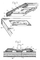
- a laminate is shown with a stripline conductor, which has the shape of a conductive band and is arranged embedded between two laminated, thin dielectric plastics sheets 2, 3 to form a first laminate, illustrated in the top part of the Figure.
- a stripline conductor which has the shape of a conductive band and is arranged embedded between two laminated, thin dielectric plastics sheets 2, 3 to form a first laminate, illustrated in the top part of the Figure.
- conductive layers in the shape of metal foils 8, 9 are applied in order to form shield and ground planes.
- the common edges of the dielectric sheets 2,3 may be sealed by a conductive layer, as is illustrated in the Figure.
- a substantially rectangular aperture or hole is arranged to form a recess 4 in the first laminate, this hole exposing a portion of the conductor.
- This exposed portion of the conductor forms one contact means 1 with a substantially flat outer surface and it has the shape of a thin band extending from one of the sides of the rectangular recess 4, is located on the inner side of the other dielectric sheet 2 and is immediately surrounded on some of its sides, in Figure 1 on three sides, by isolating inner surface portions of the other dielectric sheet 2.
- the recess 4 extends from a free edge of the first laminate, this edge also being a common edge of the dielectric sheets 2, 3.
- a corresponding contact means 5 having the shape of a thin band with a substantially flat surface is arranged on the top surface or side of a multilayer circuit pattern board forming a second laminate, this contact means 5 for instance being a selected etched portion of the conductive pattern on top of the circuit board.
- the contact means 5 may also be connected to a conductor, for instance located inside the circuit pattern board, through a metallized or through-coated hole 6 which extends between a top ground plane 7 and a lower ground plane 16 of the circuit pattern board.
- a shield and ground plane 7 surrounding laterally completely the contact means 5, this shield and ground plane for instance being another portion of the same conductive pattern as the contact means 5 of the circuit pattern board, and arranged to have its surface in essentially the same geometrical plane as the surface of the second contact means 5.
- another conductive layer 16 is located and forms another shield and ground plane.
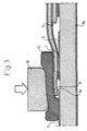
- a contact between the contact means 1, 5 is established by applying the laminated first unit and the circuit pattern board to each other, that is positioning them at each other with their large sides in engagement with each other, and by pressing the contact means 1, 5 against each other by applying a force according to the arrow 17 in Fig. 2 on top of the first laminated unit at a location opposite to the recess 4 or the first contact means 1.
- the material of laminated unit that is of the plastics sheet 2, which is left in the recess 4 will then be bent down towards the circuit board in the same time as the ground planes 7, 8, which already are engaged with each other and are located on the circuit pattern board and the laminated unit respectively, are pressed against each other in such a way that the contact area will be tightly shielded, but only in the case (not shown) where the recess 4 is located at an inner portion of the laminated unit and not extending to any of its edges.
- the press force is obtained by a suitable pressing means 10, as is illustrated in Fig. 3.
- a pad 12 is arranged between the pressing means 10 and the laminated unit, the pad 12 being made of an electrically conducting, elastic material, such as coal filled silicon rubber.
- the pad is deformed due to the pressing force and will conform to the base material, whereby said narrow portion or slit at 14 in Fig. 3, due to the aperture 4 in the plastics sheet 3, will be closed by the pad 12, which thus will cover the contact area and ensure a completely closed shield around the contact means 1, 5 in contact with the surrounding shield and ground planes 7, 9.
- the elastic pad 12 also distributes the pressure in such a way that a smooth engagement both between the contact means 1, 5 and the surrounding metal foils enclosing the contact means at three sides thereof is obtained.
- a condition for this shielding effect of the elastic pad 12 is that the edge of the top laminate where the recess 4 is located, is positioned at a distance from the edges of the lower laminate.
- the whole exposed edge, from which the recess 4 extends may be shielded by the elastic conductive pad 10.
- this edge of the first laminate may also be coated with a conductive layer, as is illustrated for the other edges in Fig. 1. Then only the common edge of the first laminate and the recess has to sealed by the elastic pad 10.
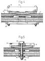
- the press force may be obtained by two bolts 19 extending through holes in both laminates and tightened by nuts 20, the bolts 19 also acting on a stiff pressing element 21 with holes for the bolts 19.
- the pressing element 21 may have a suitably shaped pressing surface which acts on the top side of the elastic pad 10 to press it into the desired contact with the ground planes 9 and 7 and also to press the contact means 1, 5 against each other.
- Another stiff element 22 may be arranged at the bottom of the circuit board, opposite to the second contact means 5, to eliminate bending of the circuit board.
- the bolts may also pass through the contact means 1, 5 and this case is illustrated in Fig. 5.
- a bolt 22 made from an isolating material passes through holes in the two laminates, in the elastic pad 10 and in a stiff element 23 arranged and acting in a similar way as the stiff element 21 of Fig. 4.
- the hole in the circuit board laminate may be a plated or metallized hole used for connection of the contact means 5 and an inner conductor 24 of the circuit board.
- An isolating nut 25 is threadedly engaged with the bolt 22 and a washer 26 may be arranged under the nut 25.
- a shielding even of the bottom of the circuit board may be obtained, as is illustrated in Fig. 6.
- a metal bolt 27 cooperating with a metal nut 28 is used and gives a pressing force in the same way as the bolt 22 of Fig. 6.
- a stiff element 29, through which the bolt 27 passes, has the shape of a large diameter washer.
- the bolt 27 should not contact the metallized hole in the circuit board and therefor an isolating sleeve 30 having a collar 31 is placed inside the metallized hole.
- this hole in the contact means 5 in circuit pattern board may have a little larger diameter than the hole through the top laminate.
- the contact means 1 of the top laminate should not extend up to this hole so that an isolating marginal portion 32 is exposed in the top dielectric sheet 2 adjacent to the hole.
- a conductive cap 33 having a hole in the centre thereof, through which the bolt 27 passes, is located at the bottom surface and has its outer portions pressed against the ground layer 16.
- this ground layer 16 is, as is conventional, removed in order to be isolated from the metallization in the through-hole.
- the conductive cap 33 has preferably a concavely shaped surface directed to said ground plane 16.
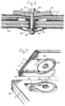
- the screw applying the pressing force may also pass the contact means 1, 5 through ordinary holes not having a metallization.
- This case is illustrated in Fig. 7 where the first contact means 1 has a circular or annular shape with a hole 34 located at its centre.
- the contact means 1 may in this case, for a conductive bolt, not reach the edge of the hole and thus an annular flat region 35 is obtained on the inner surface of the dielectric sheet 2. In this way the contact means 1 is isolated from the screw intended to pass through the hole 34.
- the contact means 1 is connected to a conductor through a connecting bridge 36.
- the contact means 5 has an elongated shape surrounding at one end a hole 37, through which the clamping screw is intended to pass.
- a through-metallized or plated hole 39 is located which thus connects the contact means 5 with signal conductors inside the circuit board.
- the contact means 5 is surrounded at all its lateral sides, that is in a geometrical plane passing through the surface of the contact means 5, by the ground plane 7.
- the shape and location of the inner edge of this surrounding ground plane 7 is adapted to fit to the recess 4 in the top laminate.
- the contact means 5 may in this case be part of the metallization deposited for the through-plating of the electrically connecting hole 39, this implying the top surface of the contact means 5 being essentially flat.
Applications Claiming Priority (3)
| Application Number | Priority Date | Filing Date | Title |
|---|---|---|---|
| SE9101836A SE468535B (sv) | 1991-06-14 | 1991-06-14 | Anordning foer kontaktering av skaermade ledningar |
| SE9101836 | 1991-06-14 | ||
| PCT/SE1992/000409 WO1992022944A1 (en) | 1991-06-14 | 1992-06-12 | A device for contacting shielded conductors |
Publications (2)
| Publication Number | Publication Date |
|---|---|
| EP0543978A1 EP0543978A1 (en) | 1993-06-02 |
| EP0543978B1 true EP0543978B1 (en) | 1996-04-24 |
Family
ID=20383044
Family Applications (1)
| Application Number | Title | Priority Date | Filing Date |
|---|---|---|---|
| EP92912771A Expired - Lifetime EP0543978B1 (en) | 1991-06-14 | 1992-06-12 | A device for contacting shielded conductors |
Country Status (7)
| Country | Link |
|---|---|
| US (1) | US5261826A (zh) |
| EP (1) | EP0543978B1 (zh) |
| JP (1) | JP3192144B2 (zh) |
| DE (1) | DE69210182T2 (zh) |
| SE (1) | SE468535B (zh) |
| TW (1) | TW236029B (zh) |
| WO (1) | WO1992022944A1 (zh) |
Families Citing this family (19)
| Publication number | Priority date | Publication date | Assignee | Title |
|---|---|---|---|---|
| US5476970A (en) * | 1984-02-16 | 1995-12-19 | Velsicol Chemical Corporation | Method for preparing aryl ketones |
| SE9301737L (sv) * | 1993-05-19 | 1994-10-24 | Ericsson Telefon Ab L M | Jordningsanordning för ett knippe skärmade kablar |
| SE503484C2 (sv) * | 1994-04-11 | 1996-06-24 | Ericsson Telefon Ab L M | Kontaktfjäder |
| US5759047A (en) * | 1996-05-24 | 1998-06-02 | International Business Machines Corporation | Flexible circuitized interposer with apertured member and method for making same |
| US5808529A (en) * | 1996-07-12 | 1998-09-15 | Storage Technology Corporation | Printed circuit board layering configuration for very high bandwidth interconnect |
| US5867371A (en) * | 1997-09-29 | 1999-02-02 | Ericsson Inc. | Cover member for sealed circuit board assembly |
| US6699395B1 (en) | 2000-10-18 | 2004-03-02 | Storage Technology Corporation | Method of forming alignment features for conductive devices |
| US6641408B1 (en) | 2000-10-18 | 2003-11-04 | Storage Technology Corporation | Compliant contacts for conductive devices |
| US6508674B1 (en) | 2000-10-18 | 2003-01-21 | Storage Technology Corporation | Multi-layer conductive device interconnection |
| US6431876B1 (en) | 2000-10-18 | 2002-08-13 | Storage Technology Corporation | Conductive trace interconnection |
| US6607394B2 (en) * | 2001-02-06 | 2003-08-19 | Optillion Ab | Hot-pluggable electronic component connection |
| KR100625976B1 (ko) * | 2003-10-16 | 2006-09-20 | 삼성에스디아이 주식회사 | 플라즈마 디스플레이 장치 |
| US7603645B2 (en) * | 2007-01-29 | 2009-10-13 | Inventec Corporation | Calibration method of insulating washer in circuit board |
| US8123572B2 (en) * | 2010-04-02 | 2012-02-28 | Tyco Electronics Corporation | Electrical components having a contact configured to engage a via of a circuit board |
| US8696378B2 (en) * | 2012-02-24 | 2014-04-15 | Tyco Electronics Corporation | Electrical connector assembly and printed circuit board configured to electrically couple to a communication cable |
| US20140017940A1 (en) * | 2012-07-11 | 2014-01-16 | Tyco Electronics Corporation | Layered connector and method of manufacturing a layered connector |
| US9912084B2 (en) * | 2014-08-20 | 2018-03-06 | Te Connectivity Corporation | High speed signal connector assembly |
| US20160146900A1 (en) * | 2014-11-24 | 2016-05-26 | Hyundai Mobis Co., Ltd. | Battery sensor assembly for vehicle |
| US10079443B2 (en) | 2016-06-16 | 2018-09-18 | Te Connectivity Corporation | Interposer socket and connector assembly |
Citations (4)
| Publication number | Priority date | Publication date | Assignee | Title |
|---|---|---|---|---|
| US3356983A (en) * | 1965-10-11 | 1967-12-05 | Ibm | Transmission line cable connector |
| US4828512A (en) * | 1986-09-25 | 1989-05-09 | G & H Technology, Inc. | Connector for flat electrical cables |
| US4911643A (en) * | 1988-10-11 | 1990-03-27 | Beta Phase, Inc. | High density and high signal integrity connector |
| US4957068A (en) * | 1988-06-09 | 1990-09-18 | Daimler-Benz Ag | Liquid-cooled four-valve cylinder head for a multi-cylinder internal combustion engine |
Family Cites Families (7)
| Publication number | Priority date | Publication date | Assignee | Title |
|---|---|---|---|---|
| GB1539470A (en) * | 1975-11-13 | 1979-01-31 | Tektronix Inc | Electrical connector |
| US4116516A (en) * | 1977-06-24 | 1978-09-26 | Gte Sylvania Incorporated | Multiple layered connector |
| US4458967A (en) * | 1982-01-15 | 1984-07-10 | Cooper Industries, Inc. | Connector for shielded flat cable |
| US4808128A (en) * | 1984-04-02 | 1989-02-28 | Amphenol Corporation | Electrical connector assembly having means for EMI shielding |
| DE3441818C1 (de) * | 1984-11-15 | 1986-02-20 | Allied Corp., Morristown, N.J. | Steckverbinder fuer ein abgeschirmtes Flachkabel |
| US4747785A (en) * | 1987-03-17 | 1988-05-31 | Global Equipment Company, Div. Of Continental Dynamics | Shielding for connector hood |
| US4975068A (en) * | 1989-12-04 | 1990-12-04 | International Business Machines | Flexible cable connector |
-
1991
- 1991-06-14 SE SE9101836A patent/SE468535B/sv not_active IP Right Cessation
-
1992
- 1992-06-12 WO PCT/SE1992/000409 patent/WO1992022944A1/en active IP Right Grant
- 1992-06-12 DE DE69210182T patent/DE69210182T2/de not_active Expired - Fee Related
- 1992-06-12 US US07/897,822 patent/US5261826A/en not_active Expired - Lifetime
- 1992-06-12 JP JP50082793A patent/JP3192144B2/ja not_active Expired - Fee Related
- 1992-06-12 EP EP92912771A patent/EP0543978B1/en not_active Expired - Lifetime
- 1992-08-13 TW TW081106418A patent/TW236029B/zh active
Patent Citations (4)
| Publication number | Priority date | Publication date | Assignee | Title |
|---|---|---|---|---|
| US3356983A (en) * | 1965-10-11 | 1967-12-05 | Ibm | Transmission line cable connector |
| US4828512A (en) * | 1986-09-25 | 1989-05-09 | G & H Technology, Inc. | Connector for flat electrical cables |
| US4957068A (en) * | 1988-06-09 | 1990-09-18 | Daimler-Benz Ag | Liquid-cooled four-valve cylinder head for a multi-cylinder internal combustion engine |
| US4911643A (en) * | 1988-10-11 | 1990-03-27 | Beta Phase, Inc. | High density and high signal integrity connector |
Also Published As
| Publication number | Publication date |
|---|---|
| DE69210182D1 (de) | 1996-05-30 |
| US5261826A (en) | 1993-11-16 |
| SE9101836D0 (sv) | 1991-06-14 |
| SE468535B (sv) | 1993-02-01 |
| DE69210182T2 (de) | 1996-09-05 |
| JP3192144B2 (ja) | 2001-07-23 |
| TW236029B (zh) | 1994-12-11 |
| SE9101836L (sv) | 1992-12-15 |
| EP0543978A1 (en) | 1993-06-02 |
| JPH06501133A (ja) | 1994-01-27 |
| WO1992022944A1 (en) | 1992-12-23 |
Similar Documents
| Publication | Publication Date | Title |
|---|---|---|
| EP0543978B1 (en) | A device for contacting shielded conductors | |
| US5828555A (en) | Multilayer printed circuit board and high-frequency circuit device using the same | |
| US6777622B2 (en) | Wiring boards | |
| US8198954B2 (en) | Impedance matched circuit board | |
| US5414223A (en) | Solder pad for printed circuit boards | |
| US5552752A (en) | Microwave vertical interconnect through circuit with compressible conductor | |
| US5631446A (en) | Microstrip flexible printed wiring board interconnect line | |
| US5375322A (en) | Method of manufacturing circuit board having lateral conductive pattern | |
| US5414220A (en) | Flexible wiring cable | |
| US5317292A (en) | Device with flexible, stripline conductors and a method of manufacturing such a device | |
| GB2272580A (en) | Shield structure for use in microwave circuit device | |
| US20030179055A1 (en) | System and method of providing highly isolated radio frequency interconnections | |
| AU1930000A (en) | Printed circuit board and method for fabricating such board | |
| US5668509A (en) | Modified coaxial to GCPW vertical solderless interconnects for stack MIC assemblies | |
| JPH04217101A (ja) | 同軸伝送線ーストリップ線結合カプラ | |
| KR20180019472A (ko) | 플렉서블 평판 케이블 및 그 제조방법 | |
| EP1195776A2 (en) | Wiring boards and processes for manufacturing wiring boards | |
| JPH0594841A (ja) | 電気コネクタ及び電気的接続方法 | |
| US5148135A (en) | Electronic hardware package | |
| JP2549125Y2 (ja) | 電気接続用コネクタ | |
| JPH04306507A (ja) | フラットケーブル | |
| JP2001035612A (ja) | Fpc/ffcコネクタ | |
| US4701723A (en) | Connection construction for electronic component | |
| KR200302854Y1 (ko) | 스플리터 | |
| JP3236984B2 (ja) | フィルタ素子を備えたコネクタ |
Legal Events
| Date | Code | Title | Description |
|---|---|---|---|
| PUAI | Public reference made under article 153(3) epc to a published international application that has entered the european phase |
Free format text: ORIGINAL CODE: 0009012 |
|
| 17P | Request for examination filed |
Effective date: 19930130 |
|
| AK | Designated contracting states |
Kind code of ref document: A1 Designated state(s): DE FR GB |
|
| 17Q | First examination report despatched |
Effective date: 19940902 |
|
| GRAH | Despatch of communication of intention to grant a patent |
Free format text: ORIGINAL CODE: EPIDOS IGRA |
|
| GRAA | (expected) grant |
Free format text: ORIGINAL CODE: 0009210 |
|
| AK | Designated contracting states |
Kind code of ref document: B1 Designated state(s): DE FR GB |
|
| REF | Corresponds to: |
Ref document number: 69210182 Country of ref document: DE Date of ref document: 19960530 |
|
| ET | Fr: translation filed | ||
| PLBE | No opposition filed within time limit |
Free format text: ORIGINAL CODE: 0009261 |
|
| STAA | Information on the status of an ep patent application or granted ep patent |
Free format text: STATUS: NO OPPOSITION FILED WITHIN TIME LIMIT |
|
| 26N | No opposition filed | ||
| REG | Reference to a national code |
Ref country code: GB Ref legal event code: IF02 |
|
| PGFP | Annual fee paid to national office [announced via postgrant information from national office to epo] |
Ref country code: GB Payment date: 20030604 Year of fee payment: 12 |
|
| PGFP | Annual fee paid to national office [announced via postgrant information from national office to epo] |
Ref country code: FR Payment date: 20030619 Year of fee payment: 12 |
|
| PGFP | Annual fee paid to national office [announced via postgrant information from national office to epo] |
Ref country code: DE Payment date: 20030630 Year of fee payment: 12 |
|
| PG25 | Lapsed in a contracting state [announced via postgrant information from national office to epo] |
Ref country code: GB Free format text: LAPSE BECAUSE OF NON-PAYMENT OF DUE FEES Effective date: 20040612 |
|
| PG25 | Lapsed in a contracting state [announced via postgrant information from national office to epo] |
Ref country code: DE Free format text: LAPSE BECAUSE OF NON-PAYMENT OF DUE FEES Effective date: 20050101 |
|
| GBPC | Gb: european patent ceased through non-payment of renewal fee |
Effective date: 20040612 |
|
| PG25 | Lapsed in a contracting state [announced via postgrant information from national office to epo] |
Ref country code: FR Free format text: LAPSE BECAUSE OF NON-PAYMENT OF DUE FEES Effective date: 20050228 |
|
| REG | Reference to a national code |
Ref country code: FR Ref legal event code: ST |