EP0537314B1 - Spulenkörper und verfahren zu seiner herstellung - Google Patents
Spulenkörper und verfahren zu seiner herstellung Download PDFInfo
- Publication number
- EP0537314B1 EP0537314B1 EP92909117A EP92909117A EP0537314B1 EP 0537314 B1 EP0537314 B1 EP 0537314B1 EP 92909117 A EP92909117 A EP 92909117A EP 92909117 A EP92909117 A EP 92909117A EP 0537314 B1 EP0537314 B1 EP 0537314B1
- Authority
- EP
- European Patent Office
- Prior art keywords
- bobbin
- section
- connections
- flattened
- coil
- Prior art date
- Legal status (The legal status is an assumption and is not a legal conclusion. Google has not performed a legal analysis and makes no representation as to the accuracy of the status listed.)
- Revoked
Links
Images




Classifications
-
- H—ELECTRICITY
- H05—ELECTRIC TECHNIQUES NOT OTHERWISE PROVIDED FOR
- H05K—PRINTED CIRCUITS; CASINGS OR CONSTRUCTIONAL DETAILS OF ELECTRIC APPARATUS; MANUFACTURE OF ASSEMBLAGES OF ELECTRICAL COMPONENTS
- H05K3/00—Apparatus or processes for manufacturing printed circuits
- H05K3/30—Assembling printed circuits with electric components, e.g. with resistors
- H05K3/32—Assembling printed circuits with electric components, e.g. with resistors electrically connecting electric components or wires to printed circuits
- H05K3/34—Assembling printed circuits with electric components, e.g. with resistors electrically connecting electric components or wires to printed circuits by soldering
- H05K3/341—Surface mounted components
- H05K3/3421—Leaded components
- H05K3/3426—Leaded components characterised by the leads
-
- H—ELECTRICITY
- H01—ELECTRIC ELEMENTS
- H01F—MAGNETS; INDUCTANCES; TRANSFORMERS; SELECTION OF MATERIALS FOR THEIR MAGNETIC PROPERTIES
- H01F5/00—Coils
- H01F5/04—Arrangements of electric connections to coils, e.g. leads
-
- H—ELECTRICITY
- H01—ELECTRIC ELEMENTS
- H01F—MAGNETS; INDUCTANCES; TRANSFORMERS; SELECTION OF MATERIALS FOR THEIR MAGNETIC PROPERTIES
- H01F5/00—Coils
- H01F5/04—Arrangements of electric connections to coils, e.g. leads
- H01F2005/046—Details of formers and pin terminals related to mounting on printed circuits
-
- Y—GENERAL TAGGING OF NEW TECHNOLOGICAL DEVELOPMENTS; GENERAL TAGGING OF CROSS-SECTIONAL TECHNOLOGIES SPANNING OVER SEVERAL SECTIONS OF THE IPC; TECHNICAL SUBJECTS COVERED BY FORMER USPC CROSS-REFERENCE ART COLLECTIONS [XRACs] AND DIGESTS
- Y02—TECHNOLOGIES OR APPLICATIONS FOR MITIGATION OR ADAPTATION AGAINST CLIMATE CHANGE
- Y02P—CLIMATE CHANGE MITIGATION TECHNOLOGIES IN THE PRODUCTION OR PROCESSING OF GOODS
- Y02P70/00—Climate change mitigation technologies in the production process for final industrial or consumer products
- Y02P70/50—Manufacturing or production processes characterised by the final manufactured product
Definitions
- the invention relates to a coil former with ends, which are injected into a lower flange, of connecting pins suitable for push-through contacting and which can be wrapped with ends of coil winding wires in a section below the lower flange.
- the invention further relates to a method for producing such a coil former.
- the boards For the conventional contacting of electronic components on assembly boards, the boards have been provided with holes, through which connecting pins protrude and on the underside of the board have been soldered to contact surfaces of printed conductor tracks through which the holes have been drilled.
- a suitable coil former with connecting pins anchored in a lower flange is known, for example, from EP-A-0 415 643.
- the surface contacting of such mounting plates is becoming increasingly common, in which the components are placed directly on contact surfaces of the plate and soldered there. If necessary, the component can also be fixed on the plate by gluing.
- the components For this type of contacting, the components must be provided with suitable connections.
- strip-shaped connections are regularly used, which are anchored in the housing of the component and are angled outside the housing.
- connections are routed laterally out of the housing, angled downwards and then outwards again. It has been shown that automatic assembly of a component formed with a thermosetting material, for example a thermosetting coil former, cannot be realized with such metal strips, since the sealing of the tool does not succeed, so that thermosetting material always escapes, which in a subsequent machining operation from Component must be removed again.
- the connections formed from sheet metal strips are in use susceptible to a bobbin during winding of the bobbin and deform slightly in the direction of the bends, so that the connections with their ends bent outward no longer lie flat on the contact surface and therefore no longer guarantee reliable contacting.
- the invention has for its object to provide a bobbin that largely avoids the disadvantages described above.
- connection pins are flattened below the section to form a rectangular cross section and are angled in the region of the flattened cross section to form surface-mountable connections.
- the stated object is also achieved with a method for producing a coil former, in which a conventional, for the push-through technique usable pin is anchored in conventional technology in the lower flange of the coil body, in which the free end of the part of the connecting pin protruding from the flange is flattened below the section of the connecting pin provided for wrapping and in which the flattened part of the connecting pin is used for Forming a surface mountable connector is angled.
- the invention has the advantage that a coil former for surface contacting can be produced in the same way as a coil former for the conventional push-through connection technology and that the pins that can be used for the push-through technology can then be flattened and bent over, so that a suitable one for surface mounting can then be used Component is created. It is therefore possible to produce the bobbin for the previous push-through contact and the surface contact in basically the same way and to provide connections. It is then only necessary to subsequently process the connections of the coil former provided for surface mounting and to form them in the manner mentioned. Furthermore, there is the advantage that the connections in the form of connecting pins can be led out downward from the coil body and then bent. Compared to the lateral lead-out of strip-shaped connections, which are first bent downwards and then outwards again, there is a considerable saving in the space required on the plate, which can be up to a third in the case of small coil formers.
- a coil former according to the invention is particularly advantageous because a stable section of the connection is available for winding with the end of the coil wire, so that the connection is mechanically less susceptible to one Bending when making the connection is.
- the part of the connection protruding from the coil former is designed with a square cross section before the flattening, a particularly favorable geometry for winding the coil wire is ensured in a known manner.
- wire-shaped connecting pins for example in the manufacture of a coil former, takes place in the injection mold in conventional technology and does not pose any problems. According to the invention, therefore, it is not necessary to handle expensive and new connecting pins with modified cross sections, which may have to be aligned and fed in a specific position, which further increases the outlay.
- connections which are located on at least two outer sides of the coil body
- connections are flattened out by positioning a counter-holder on the inside of the connections and pressing them from the outside against the stationary counter-holder with a press ram.
- the counter-holder will be moved as one piece between the connections and then the ram will press the connections against the counter-holder from the outside, whereby the desired deformation in the sense of flattening takes place.
- the invention not only allows the use of the same manufacturing process and the use of the same housing for the bobbin, if necessary, but also the use of identical automatic winding machines.
- the method according to the invention can be carried out without exerting greater forces on the coil former itself, so that the anchoring of the connections therein is not loaded in a risky manner when the connecting pins are subsequently deformed.
- connections according to the invention can be produced very precisely. For example, it is possible to bend the flattened connector pin in such a way that a small angle is formed between the contact surface and the contact surface of the connector, as a result of which the soldering material flows better into the area of the connector due to a certain capillary action, which increases the security of the connector Solder connection leads.
- FIG. 1 shows a connection 1 which is anchored in a coil former 2. This is generally done by inserting the connector into an injection mold for the manufacture of this component and thus partially injecting it during the manufacture of the coil former, for example as a plastic component.
- the connection consists of a pin 3 with a round cross section, as can be seen from the illustration of section S2 in FIG. 1.
- the pin 3 in section 4 is embossed into a square with a square cross section, as can be seen from the representation of the section S1.
- the connector 1 is anchored in the coil body with a round base 5.
- the connection 1 in the form shown in FIG. 1a is a conventional pin 3, as is used for the conventional push-through contact.
- the connector pin 3 is shortened in a first step by cutting off one end, as shown in FIG. 1b.
- the shortening takes place at a distance below the square area 4 in the area of the round cross section S2.
- connection piece 6 is subjected to flattening by a pressing process, as a result of which, below a remaining piece of the square area 4, there remains a connection piece 6 with a rectangular cross section, the cross section of which is shown as section S3 in FIG. 1.
- FIG. 1c shows that the deformation to the rectangular cross section according to S3 has essentially been effected by a pressing movement from the outside inwards against a fixed counter bearing on the inside of the connection 1.
- the connector 6 is bent at a distance from the remaining square area 4 substantially at right angles to the outside, an acute angle being advantageous compared to a flat contact surface.
- the remaining square area 4 can advantageously be wrapped with the ends of a coil winding wire in order to establish the electrical connection to the coil. The winding takes place in the stable square area 4, so that the bent connecting part 6 is not affected by the winding process.
- FIG. 2 shows the state according to FIG. 1a on a coil former 2 as an electronic component.
- the terminals 1 designed as pins are injected into the flanges 2 'of the coil body 2.
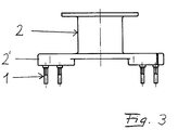
- FIG. 3 shows the state of the connections 1 after shortening the connection pins 3 according to FIG. 1b.
- FIG. 4 illustrates the flattening of the connections 1 according to FIG. 1c, it becoming clear that the material has been displaced from the outside in, that is to say a press ram has moved from the outside inwards against a counter-holder arranged on the inside.
- FIG. 5 shows the state after the connections 1 have been bent outwards from the center of the coil former.
- Figure 6 illustrates that the flanges 2 'of the bobbin 2 are attached laterally and there, for example, each carry three connections 1.
- a counterholder can be inserted from below against the connections 1, the outer contour of which is adapted to the position of the connections 1.
- press rams can be pressed from the outside against the connections 1 in order to produce the flattening according to FIG.
Landscapes
- Engineering & Computer Science (AREA)
- Power Engineering (AREA)
- Manufacturing & Machinery (AREA)
- Microelectronics & Electronic Packaging (AREA)
- Manufacturing Cores, Coils, And Magnets (AREA)
- Manufacturing Of Electrical Connectors (AREA)
- Electromagnets (AREA)
- Yarns And Mechanical Finishing Of Yarns Or Ropes (AREA)
- Coils Or Transformers For Communication (AREA)
Description
- Die Erfindung betrifft einen Spulenkörper mit in einem unteren Flansch eingespritzten Enden von zur Durchsteckkontaktierung geeigneten Anschlußstiften, die in einem Abschnitt unterhalb des unteren Flansches mit Enden von Spulenwickeldrähten umwikkelbar sind. Die Erfindung betrifft ferner ein Verfahren zur Herstellung eines solchen Spulenkörpers.
- Für die herkömmliche Kontaktierung von elektronischen Bauelementen auf Bestückungsplatten sind die Platten mit Bohrungen versehen worden, durch die Anschlußstifte hindurchragten und auf der Unterseite der Platte mit von den Bohrungen durchbohrten Kontaktflächen von gedruckten Leiterbahnen verlötet wurden. Ein dafür geeigneter Spulenkörper mit in einem unteren Flansch verankerten Anschlußstiften ist z.B. aus EP-A-0 415 643 bekannt. Demgegenüber setzt sich zunehmend die Oberflächenkontaktierung solcher Bestückungsplatten durch, bei der die Bauelemente unmittelbar auf Kontaktflächen der Platte aufgesetzt und dort verlötet werden. Gegebenenfalls kann das Bauelement auf der Platte durch Aufkleben zusätzlich fixiert werden. Für diese Art der Kontaktierung müssen die Bauelemente mit geeigneten Anschlüssen versehen sein. Hierzu werden regelmäßig streifenförmige Anschlüsse verwendet, die in dem Gehäuse des Bauelements verankert werden und außerhalb des Gehäuses abgewinkelt sind. Regelmäßig werden diese Anschlüsse seitlich aus dem Gehäuse herausgeführt, nach unten und anschließend wieder nach außen abgewinkelt. Es hat sich gezeigt, daß eine automatische Bestückung von mit einem Duroplasten gebildeten Bauteil, beispielsweise einem duroplastischen Spulenkörper, mit derartigen Blechstreifen nicht zu realisieren ist, da die Abdichtung des Werkzeugs nicht gelingt, so daß immer duroplastisches Material austritt, das in einem anschließenden Bearbeitungsvorgang vom Bauelement wieder entfernt werden muß. Darüber hinaus sind die aus Blechstreifen gebildeten Anschlüsse bei einer Verwendung an einem Spulenkörper bei der Bewicklung des Spulenkörpers anfällig und verformen sich leicht in Richtung der Biegungen, so daß die Anschlüsse mit ihren nach außen abgebogenen Enden nicht mehr plan auf der Kontaktfläche aufliegen und daher keine sichere Kontaktierung mehr gewährleisten.
- Es ist auch bekannt, herkömmliche Gehäuse mit streifenförmigen Anschlußbeinen, die in eine passende Fassung einsteckbar sind, dadurch oberflächenmontierbar zu machen, daß die Anschlußbeine umgebogen werden. Hierdurch entsteht eine den oben erwähnten streifenförmigen Anschlüssen für die Oberflächenmontage vergleichbare Anordnung.
- Aufgrund der Probleme mit den bekannten streifenförmigen Anschlüssen ist vorgeschlagen worden, die Anschlüsse von oberflächenmontierbaren Bauelementen durch Stifte mit einem relativ großen Querschnitt und einem im Querschnitt stufenförmig erweiterten unteren Ende (das im Höhenschnitt eine T-Form verursacht) durchzuführen. Der hierfür erforderliche Kostenaufwand ist hoch und für die große Anzahl der benötigten Anschlüsse wirtschaftlich nicht zu realisieren.
- Der Erfindung liegt die Aufgabe zugrunde, einen Spulenkörper zu schaffen, der die oben beschriebenen Nachteile weitgehend vermeidet.
- Diese Aufgabe wird erfindungsgemäß mit einem Spulenkörper der eingangs erwähnten Art gelöst, der dadurch gekennzeichnet ist, daß die Anschlußstifte unterhalb des Abschnitts zu einem rechteckigen Querschnitt abgeplattet und im Bereich des abgeplatteten Querschnitts zur Bildung von oberflächenmontierbaren Anschlüssen abgewinkelt sind.
- Die genannte Aufgabe wird ferner mit einem Verfahren zur Herstellung eines Spulenkörpers gelöst, bei dem ein herkömmlicher, für die Durchstecktechnik verwendbarer Stift in herkömmlicher Technik im unteren Flansch des Spulenkörpers verankert wird, bei dem das freie Ende des aus dem Flansch herausstehenden Teils des Anschlußstifts unterhalb des zur Umwicklung vorgesehenen Abschnitts des Anschlußstifts durch Pressen abgeplattet wird und bei dem der abgeplattete Teil des Anschlußstifts zur Bildung eines oberflächenmontierbaren Anschlusses abgewinkelt wird.
- Die Erfindung bietet den Vorteil, daß ein Spulenkörper für die Oberflächenkontaktierung prinzipiell in gleicher Weise wie ein Spulenkörper für die herkömmliche Durchsteck-Verbindungstechnik herstellbar ist und daß anschließend die für die Durchstecktechnik verwendbaren Stifte abgeplattet und umgebogen werden können, so daß dann ein für die Oberflächenmontage geeignetes Bauelement geschaffen ist. Es ist daher möglich, die Spulenkörper für die bisherige Durchsteckkontaktierung und die Oberflächenkontaktierung in prinzipiell der gleichen Weise herzustellen und mit Anschlüssen zu versehen. Dabei ist es lediglich erforderlich, die Anschlüsse des für die Oberflächenmontage vorgesehenen Spulenkörpers anschließend zu bearbeiten und in der erwähnten Weise auszubilden. Des weiteren ergibt sich der Vorteil, daß die Anschlüsse in Form von Anschlußstiften nach unten aus dem Spulenkörper herausgeführt und dann abgebogen sein können. Gegenüber der seitlichen Herausführung von streifenförmigen Anschlüssen, die zunächst nach unten und dann wieder nach außen abgebogen sind, ergibt sich eine erhebliche Einsparung des auf der Platte benötigten Platzes, die bei kleinen Spulenkörpern bis zu einem Drittel betragen kann.
- Die erfindungsgemäße Ausbildung eines Spulenkörpers ist besonders vorteilhaft, weil ein stabiler Abschnitt des Anschlusses für die Umwicklung mit dem Ende des Spulendrahts zur Verfügung steht, so daß der Anschluß mechanisch wenig anfällig gegen eine Verbiegung bei der Herstellung des Anschlusses ist. Bei einer Ausbildung des aus dem Spulenkörper herausragenden Teils des Anschlusses mit einem quadratischen Querschnitt vor der Abplattung wird in bekannter Weise eine besonders günstige Geometrie für das Anwickeln des Spulendrahtes gewährleistet.
- Die Zuführung drahtförmiger Anschlußstifte beispielsweise bei der Herstellung eines Spulenkörpers in die Spritzform geschieht in der herkömmlichen Technik und wirft keine Probleme auf. Es müssen daher erfindungsgemäß nicht teure und neue Anschlußstifte mit veränderten Querschnitten gehandhabt werden, die gegebenenfalls ausgerichtet und in einer bestimmten Lage zugeführt werden müssen, wodurch der Aufwand noch vergrößert wird.
- Besonders vorteilhaft ist es, wenn die Anschlüsse, die sich an mindestens zwei Außenseiten des Spulenkörpers befinden, dadurch abgeplattet werden, daß an der Innenseite der Anschlüsse ein Gegenhalter positioniert und mit einem Preßstempel von außen gegen den ortsfest gehaltenen Gegenhalter gedrückt werden. Dadurch bildet sich durch die Abplattung eine Stufe an der Außenseite des Anschlusses aus. Im allgemeinen wird der Gegenhalter dabei als ein Stück zwischen die Anschlüsse gefahren werden und anschließend die Preßstempel von außen die Anschlüsse gegen den Gegenhalter drücken, wodurch die gewünschte Verformung im Sinne der Abplattung erfolgt. Die Erfindung erlaubt nicht nur die Verwendung eines gleichen Herstellungsverfahrens und die Verwendung gegebenenfalls gleicher Gehäuse für die Spulenkörper, sondern bei deren auch die Verwendung identischer Wickelautomaten. Das erfindungsgemäße Verfahren ist ohne die Ausübung größerer Kräfte auf den Spulenkörper selbst ausführbar, so daß die Verankerung der Anschlüsse darin bei einer anschließenden Verformung der Anschlußstifte nicht in riskanter Weise belastet wird.
- Die erfindungsgemäßen Anschlüsse lassen sich sehr präzise herstellen. So ist es beispielsweise möglich, die Abwinkelung des abgeplatteten Anschlußstiftes so durchzuführen, daß zwischen der Kontaktfläche und der Auflagefläche des Anschlusses ein kleiner Winkel ausgebildet wird, wodurch das Lötmaterial aufgrund einer gewissen Kapillarwirkung verbessert in den Bereich des Anschlusses einfließt, das zu einer erhöhten Sicherheit der Lötverbindung führt.
- Die Erfindung wird im folgenden anhand von in der Zeichnung dargestellten Ausführungsbeispielen näher erläutert. Es zeigt:
- Figur 1 -
- einen in ein Bauelement eingebetteten Anschlußstift in vier Bearbeitungsphasen
- Figur 2 -
- eine Seitenansicht eines Spulenkörpers mit verankerten Anschlußstiften
- Figur 3 -
- den Spulenkörper gemäß Figur 2 mit gekürzten Anschlußstiften
- Figur 4 -
- den Spulenkörper gemäß Figur 3 nach einer Abplattung der Anschlußstifte durch einen Preßvorgang
- Figur 5 -
- den Spulenkörper mit nach außen abgewinkelten Anschlüssen
- Figur 6 -
- eine Draufsicht auf den Spulenkörper gemäß Figur 5.
- Figur 1 zeigt einen Anschluß 1, der in einem Spulenkörper 2 verankert ist. Dies geschieht im allgemeinen dadurch, daß bei der Herstellung des z.B. als Kunststoff-Bauelement vorliegenden Spulenkörpers der Anschluß in eine Spritzform für die Herstellung dieses Bauelements eingelegt und somit teilweise eingespritzt wird. Im vorliegenden Fall besteht der Anschluß aus einem Stift 3 mit einem runden Querschnitt, wie er sich aus der Darstellung des Schnittes S2 in Figur 1 ergibt. Am oberen Ende ist der Stift 3 im Abschnitt 4 zu einem Vierkant mit quadratischem Querschnitt geprägt, wie er aus der Darstellung des Schnittes S1 hervorgeht. Mit einem runden Sockel 5 ist der Anschluß 1 in dem Spulenkörper verankert. Der Anschluß 1 ist in der in Figur 1a dargestellten Form ein üblicher Stift 3, wie er für die herkömmliche Durchsteck-Kontaktierung eingesetzt wird.
- Zur Verwendung eines solchen Anschlusses 1 für eine Oberflächenmontage wird in einem ersten Schritt der Anschlußstift 3 durch Abschneiden eines Endes gekürzt, wie dies in Figur 1b gezeigt ist. Das Kürzen erfolgt mit Abstand unterhalb des Vierkantbereichs 4 im Bereich des runden Querschnitts S2.
- Im folgenden Verfahrensschritt wird das freie Ende des Anschlusses 1 einer Abplattung durch einen Preßvorgang unterworfen, wodurch unterhalb eines verbleibenden Stückes des Vierkantbereichs 4 ein im Querschnitt rechteckiges Anschlußstück 6 verbleibt, dessen Querschnitt als Schnitt S3 in Figur 1 dargestellt ist. Figur 1c läßt erkennen, daß die Verformung zu dem rechteckigen Querschnitt gemäß S3 im wesentlichen durch eine Preßbewegung von außen nach innen gegen ein feststehendes Gegenlager auf der Innenseite des Anschlusses 1 erfolgt ist.
- Im Anschluß daran wird das Anschlußstück 6 mit Abstand von dem verbliebenen Vierkantbereich 4 im wesentlichen rechtwinkelig nach außen abgebogen, wobei ein spitzer Winkel gegenüber einer ebenen Auflagefläche vorteilhaft ist. Der verbliebene Vierkantbereich 4 läßt sich mit Vorteil mit den Enden eines Spulenwickeldrahtes umwickeln, um die elektrische Verbindung zur Spule herzustellen. Die Umwicklung erfolgt in dem stabilen Vierkantbereicht 4, so daß das gebogene Anschlußteil 6 durch den Wickelvorgang nicht beeinträchtigt wird.
- Figur 2 zeigt den Zustand gemäß Figur 1a an einem Spulenkörper 2 als elektronisches Bauelement. Die als Anschlußstifte ausgebildeten Anschlüsse 1 sind in angesetzten Flanschen 2′ des Spulenkörpers 2 eingespritzt.
- Figur 3 zeigt den Zustand der Anschlüsse 1 nach dem Kürzen der Anschlußstifte 3 gemäß Figur 1b.
- Figur 4 verdeutlicht die Abplattung der Anschlüsse 1 gemäß Figur 1c, wobei deutlich wird, daß die Materialverdrängung von außen nach innen erfolgt ist, also ein Preßstempel sich von außen nach innen gegen einen innen angeordneten Gegenhalter bewegt hat.
- Figur 5 zeigt den Zustand nach dem Abbiegen der Anschlüsse 1 von der Mitte des Spulenkörpers nach außen.
- Figur 6 verdeutlicht, daß die Flansche 2′ des Spulenkörpers 2 seitlich angesetzt sind und dort beispielsweise jeweils drei Anschlüsse 1 tragen. Gegen die Anschlüsse 1 kann nach dem Kürzen gemäß Figur 3 auf der Innenseite von unten ein Gegenhalter eingefahren werden, dessen Außenkontur der Position der Anschlüsse 1 angepaßt ist. Sodann können von außen Preßstempel gegen die Anschlüsse 1 gedrückt werden, um die Abplattung gemäß Figur 4 herzustellen.
Claims (7)
- Spulenkörper mit in einem unteren Flansch (2′) eingespritzten Enden (5) von zur Durchsteckkontaktierung geeigneten Anschlußstiften (3), die in einem Abschnitt (4) unterhalb des unteren Flansches (2′) mit Enden von Spulenwickeldrähten umwickelbar sind, dadurch gekennzeichnet, daß die Anschlußstifte (3) unterhalb des Abschnitts (4) zu einem rechteckigen Querschnitt (S3) abgeplattet und im Bereich des abgeplatteten Querschnitts (S3) zur Bildung von oberflächenmontierbaren Anschlüssen (1) abgewinkelt sind.
- Spulenkörper nach Anspruch 1, dadurch gekennzeichnet, daß die Anschlüsse (1) von der Mitte des Spulenkörpers (2) aus im wesentlichen rechtwinkelig nach außen abgewinkelt sind.
- Spulenkörper nach Anspruch 1 oder 2, dadurch gekennzeichnet, daß durch die Abplattung eine Stufe nur an der Außenseite des Anschlusses (1) ausgebildet ist.
- Spulenkörper nach einem der Ansprüche 1 bis 3, dadurch gekennzeichnet, daß der umwickelbare Abschnitt (4) zu einem quadratischen Querschnitt (S1) geformt ist.
- Verfahren zur Herstellung eines Spulenkörpers bei welchem ein herkömmlicher, für die Durchstecktechnik verwendbarer Stift (3) in herkömmlicher Technik im unteren Flansch (2′) des Spulenkörpers (2) verankert wird, dadurch gekennzeichnet, daß das freie Ende (6) des aus dem Flansch (2′) herausstehenden Teils des Anschlußstifts (3) unterhalb des zur Umwicklung vorgesehenen Abschnitts (4) des Anschlußstifts (3) durch Pressen abgeplattet wird und daß der abgeplattete Teil (6) des Anschlußstifts (1) zur Bildung eines oberflächenmontierbaren Anschlusses (1) abgewinkelt wird.
- Verfahren nach Anspruch 5, bei dem sich die Anschlüsse (1) auf wenigstens zwei Außenseiten des Spulenkörpers (2) befinden, wobei an der Innenseite der Anschlußstifte (3) ein Gegenhalter positioniert wird und mit einem Preßstempel die Anschlußstifte (3) von außen gegen den ortsfest gehaltenen Gegenhalter gedrückt werden.
- Verfahren nach Anspruch 5 oder 6, dadurch gekennzeichnet, daß der Anschlußstift (3) vor dem Pressen gekürzt wird.
Applications Claiming Priority (3)
| Application Number | Priority Date | Filing Date | Title |
|---|---|---|---|
| DE4114391A DE4114391C2 (de) | 1991-05-03 | 1991-05-03 | Spulenkörper und Verfahren zu seiner Herstellung |
| DE4114391 | 1991-05-03 | ||
| PCT/DE1992/000335 WO1992020079A1 (de) | 1991-05-03 | 1992-04-23 | Spulenkörper und verfahren zu seiner herstellung |
Publications (2)
| Publication Number | Publication Date |
|---|---|
| EP0537314A1 EP0537314A1 (de) | 1993-04-21 |
| EP0537314B1 true EP0537314B1 (de) | 1995-11-29 |
Family
ID=6430856
Family Applications (1)
| Application Number | Title | Priority Date | Filing Date |
|---|---|---|---|
| EP92909117A Revoked EP0537314B1 (de) | 1991-05-03 | 1992-04-23 | Spulenkörper und verfahren zu seiner herstellung |
Country Status (5)
| Country | Link |
|---|---|
| EP (1) | EP0537314B1 (de) |
| AT (1) | ATE130953T1 (de) |
| CA (1) | CA2086669A1 (de) |
| DE (2) | DE4114391C2 (de) |
| WO (1) | WO1992020079A1 (de) |
Families Citing this family (3)
| Publication number | Priority date | Publication date | Assignee | Title |
|---|---|---|---|---|
| DE19512343C1 (de) * | 1995-04-01 | 1996-01-25 | Hohenloher Spulenkoerper | Spulenkörper mit Anschlußstiften hoher Auszugsfestigkeit sowie Verfahren zur Herstellung der Stifte |
| US5796324A (en) * | 1996-11-12 | 1998-08-18 | Delco Electronics Corporation | Surface mount coil assembly |
| DE102015211734B4 (de) | 2015-06-24 | 2025-09-25 | SUMIDA Components & Modules GmbH | SMD-Bauelement |
Family Cites Families (7)
| Publication number | Priority date | Publication date | Assignee | Title |
|---|---|---|---|---|
| JPS4820653U (de) * | 1971-07-19 | 1973-03-08 | ||
| DE3227645A1 (de) * | 1982-07-23 | 1984-01-26 | Siemens AG, 1000 Berlin und 8000 München | Elektronisches bauelement und verfahren zu dessen herstellung |
| NL8300513A (nl) * | 1983-02-11 | 1984-09-03 | Philips Nv | Hoogfrequentspoel met aansluitpennen. |
| DE3480140D1 (en) * | 1984-07-25 | 1989-11-23 | Matsushita Electric Industrial Co Ltd | Electronic component |
| EP0182068A3 (de) * | 1984-10-08 | 1987-02-04 | Roederstein Spezialfabriken für Bauelemente der Elektronik und Kondensatoren der Starkstromtechnik GmbH | Oberflächenmontagekondensator |
| DE8904003U1 (de) * | 1989-03-30 | 1989-05-18 | Siemens AG, 1000 Berlin und 8000 München | Induktives Bauelement zur Montage auf einer Leiterplatte |
| US5008644A (en) * | 1989-08-31 | 1991-04-16 | At&T Bell Laboratories | Terminal assembly for linear magnetic component bobbin |
-
1991
- 1991-05-03 DE DE4114391A patent/DE4114391C2/de not_active Expired - Fee Related
-
1992
- 1992-04-23 EP EP92909117A patent/EP0537314B1/de not_active Revoked
- 1992-04-23 CA CA002086669A patent/CA2086669A1/en not_active Abandoned
- 1992-04-23 AT AT92909117T patent/ATE130953T1/de not_active IP Right Cessation
- 1992-04-23 DE DE59204493T patent/DE59204493D1/de not_active Revoked
- 1992-04-23 WO PCT/DE1992/000335 patent/WO1992020079A1/de not_active Ceased
Also Published As
| Publication number | Publication date |
|---|---|
| DE59204493D1 (de) | 1996-01-11 |
| DE4114391A1 (de) | 1992-11-05 |
| ATE130953T1 (de) | 1995-12-15 |
| DE4114391C2 (de) | 1994-10-20 |
| EP0537314A1 (de) | 1993-04-21 |
| CA2086669A1 (en) | 1992-11-04 |
| WO1992020079A1 (de) | 1992-11-12 |
Similar Documents
| Publication | Publication Date | Title |
|---|---|---|
| DE69528322T2 (de) | Drosselspule und Verfahren zu seiner Herstellung | |
| DE3228581C2 (de) | Kleinformatige Kontaktstift-Baugruppe | |
| DE68920185T2 (de) | Vorrichtung zur Verbindung von elektrischen Drähten mit Leiterdrähten. | |
| EP0863530A2 (de) | Leiterplatte für elektrische Schaltungen und Verfahren zur Herstellung einer solchen Leiterplatte | |
| DE69023190T2 (de) | Anschlusszusammenbau für die Spule einer linearen Magnetkomponente. | |
| DE3010876A1 (de) | Verfahren zur herstellung einer leiterplatte | |
| EP1128476B2 (de) | Verfahren zur Herstellung eines Steckverbinders | |
| EP0175069A1 (de) | Verfahren zur Herstellung eines induktiven Bauelements mit einem bewickelten Ringbandkern | |
| DE69210694T2 (de) | Herstellungsverfahren für Druckanschlussklemme | |
| DE4310369A1 (de) | Adapter | |
| EP0811995B1 (de) | Magnetspule sowie Verfahren zu deren Herstellung | |
| DE4114391C2 (de) | Spulenkörper und Verfahren zu seiner Herstellung | |
| EP0513010B1 (de) | Elektromagnetisches relais | |
| EP0763843B1 (de) | Elektrisches Bauelement, insbesondere relais, und Verfahren zu dessen Einbau in eine Leiterplatte | |
| DE3430589C2 (de) | ||
| DE19813527C1 (de) | SMD-Kunststoffkörper für Bauelemente | |
| DE29813650U1 (de) | Verbindungsstifte für eine Transformatorspule | |
| EP0082238A1 (de) | Relais | |
| DE2348674A1 (de) | Verfahren zum herstellen von elektrischen steckverbindern | |
| DE69516704T2 (de) | Lottragender anschlussdraht und verfahren zu seiner herstellung und verwendung | |
| DE2810511C2 (de) | Adapter für ein elektrisches Bauelement, insbesondere für ein Relais, und Verfahren zu dessen Herstellung | |
| DE1936422A1 (de) | Elektrischer Durchgangleiter in Stiftform | |
| DE2321041A1 (de) | Elektrische klemme mit einem stift fuer drahtwickelverbindungen | |
| DE3936110C2 (de) | Lötstift mit Anwickelscheren für Hochtemperaturlackdrähte | |
| DE3244628A1 (de) | Elektrischer spulenkoerper |
Legal Events
| Date | Code | Title | Description |
|---|---|---|---|
| PUAI | Public reference made under article 153(3) epc to a published international application that has entered the european phase |
Free format text: ORIGINAL CODE: 0009012 |
|
| 17P | Request for examination filed |
Effective date: 19921208 |
|
| AK | Designated contracting states |
Kind code of ref document: A1 Designated state(s): AT BE CH DE FR GB IT LI NL SE |
|
| 17Q | First examination report despatched |
Effective date: 19950209 |
|
| GRAA | (expected) grant |
Free format text: ORIGINAL CODE: 0009210 |
|
| AK | Designated contracting states |
Kind code of ref document: B1 Designated state(s): AT BE CH DE FR GB IT LI NL SE |
|
| REF | Corresponds to: |
Ref document number: 130953 Country of ref document: AT Date of ref document: 19951215 Kind code of ref document: T |
|
| GBT | Gb: translation of ep patent filed (gb section 77(6)(a)/1977) |
Effective date: 19951130 |
|
| REF | Corresponds to: |
Ref document number: 59204493 Country of ref document: DE Date of ref document: 19960111 |
|
| REG | Reference to a national code |
Ref country code: CH Ref legal event code: NV Representative=s name: ANDRE BRAUN PATENTANWALT VSP |
|
| ITF | It: translation for a ep patent filed | ||
| ET | Fr: translation filed | ||
| PLBI | Opposition filed |
Free format text: ORIGINAL CODE: 0009260 |
|
| PLBF | Reply of patent proprietor to notice(s) of opposition |
Free format text: ORIGINAL CODE: EPIDOS OBSO |
|
| 26 | Opposition filed |
Opponent name: SIEMENS AG Effective date: 19960823 |
|
| NLR1 | Nl: opposition has been filed with the epo |
Opponent name: SIEMENS AG |
|
| PLBF | Reply of patent proprietor to notice(s) of opposition |
Free format text: ORIGINAL CODE: EPIDOS OBSO |
|
| PLBF | Reply of patent proprietor to notice(s) of opposition |
Free format text: ORIGINAL CODE: EPIDOS OBSO |
|
| RAP2 | Party data changed (patent owner data changed or rights of a patent transferred) |
Owner name: HOHENLOHER KUNSTSTOFFTECHNIK GMBH & CO. |
|
| NLT2 | Nl: modifications (of names), taken from the european patent patent bulletin |
Owner name: HOHENLOHER KUNSTSTOFFTECHNIK GMBH & CO. |
|
| PGFP | Annual fee paid to national office [announced via postgrant information from national office to epo] |
Ref country code: SE Payment date: 19980406 Year of fee payment: 7 |
|
| PGFP | Annual fee paid to national office [announced via postgrant information from national office to epo] |
Ref country code: GB Payment date: 19980415 Year of fee payment: 7 |
|
| PGFP | Annual fee paid to national office [announced via postgrant information from national office to epo] |
Ref country code: DE Payment date: 19980418 Year of fee payment: 7 |
|
| PGFP | Annual fee paid to national office [announced via postgrant information from national office to epo] |
Ref country code: FR Payment date: 19980424 Year of fee payment: 7 |
|
| PGFP | Annual fee paid to national office [announced via postgrant information from national office to epo] |
Ref country code: AT Payment date: 19980427 Year of fee payment: 7 |
|
| PGFP | Annual fee paid to national office [announced via postgrant information from national office to epo] |
Ref country code: NL Payment date: 19980430 Year of fee payment: 7 |
|
| PGFP | Annual fee paid to national office [announced via postgrant information from national office to epo] |
Ref country code: BE Payment date: 19980512 Year of fee payment: 7 |
|
| PGFP | Annual fee paid to national office [announced via postgrant information from national office to epo] |
Ref country code: CH Payment date: 19980526 Year of fee payment: 7 |
|
| RDAH | Patent revoked |
Free format text: ORIGINAL CODE: EPIDOS REVO |
|
| RDAG | Patent revoked |
Free format text: ORIGINAL CODE: 0009271 |
|
| 27W | Patent revoked |
Effective date: 19980816 |
|
| GBPR | Gb: patent revoked under art. 102 of the ep convention designating the uk as contracting state |
Free format text: 980816 |
|
| REG | Reference to a national code |
Ref country code: CH Ref legal event code: PL |
|
| NLR2 | Nl: decision of opposition |