EP0536635B1 - Masque à rayons X, méthode de fabrication et d'exposition - Google Patents
Masque à rayons X, méthode de fabrication et d'exposition Download PDFInfo
- Publication number
- EP0536635B1 EP0536635B1 EP92116781A EP92116781A EP0536635B1 EP 0536635 B1 EP0536635 B1 EP 0536635B1 EP 92116781 A EP92116781 A EP 92116781A EP 92116781 A EP92116781 A EP 92116781A EP 0536635 B1 EP0536635 B1 EP 0536635B1
- Authority
- EP
- European Patent Office
- Prior art keywords
- ray
- film
- stress
- mask structure
- absorber
- Prior art date
- Legal status (The legal status is an assumption and is not a legal conclusion. Google has not performed a legal analysis and makes no representation as to the accuracy of the status listed.)
- Expired - Lifetime
Links
Images


Classifications
-
- G—PHYSICS
- G03—PHOTOGRAPHY; CINEMATOGRAPHY; ANALOGOUS TECHNIQUES USING WAVES OTHER THAN OPTICAL WAVES; ELECTROGRAPHY; HOLOGRAPHY
- G03F—PHOTOMECHANICAL PRODUCTION OF TEXTURED OR PATTERNED SURFACES, e.g. FOR PRINTING, FOR PROCESSING OF SEMICONDUCTOR DEVICES; MATERIALS THEREFOR; ORIGINALS THEREFOR; APPARATUS SPECIALLY ADAPTED THEREFOR
- G03F1/00—Originals for photomechanical production of textured or patterned surfaces, e.g., masks, photo-masks, reticles; Mask blanks or pellicles therefor; Containers specially adapted therefor; Preparation thereof
- G03F1/22—Masks or mask blanks for imaging by radiation of 100nm or shorter wavelength, e.g. X-ray masks, extreme ultraviolet [EUV] masks; Preparation thereof
Definitions
- the present invention relates to an X-ray mask structure used in lithography when fine patterns for large-scale integrated (LSI) circuits, micromachines or the like are printed on wafers or the like by X-ray exposure, an X-ray exposure method and a method of manufacturing the X-ray mask structure.
- LSI large-scale integrated
- Fig. 2 is a sectional view illustrating a commonly used X-ray mask structure.
- reference numeral 21 denotes a silicon frame for holding an X-ray permeable film
- reference numeral 22 denotes an X-ray permeable film
- reference numeral 23 denotes an X-ray absorber.
- Silicon (Si), silicon nitride (SiN), silicon carbide (SiC) or the like is used for the X-ray permeable film.
- Gold (Au), tantalum (Ta), tungsten (W) or the like is used as an X-ray absorber.
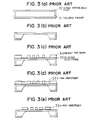
- Fig. 3 shows an example of a conventional method of manufacturing X-ray mask structures, in which an Au plated film is used as an X-ray absorber.
- An X-ray permeable film 32 is formed by CVD (Chemical Vapor Deposition) to a thickness of 1 to 3 ⁇ m on an Si substrate 31 having a thickness of 1 to 5 mm (Fig. 3a).
- the reverse surface thereof is etched by a potassium hydroxide solution or the like, so that a window is opened (Fig. 3b).
- a plating electrode 35 is formed on the X-ray permeable film, a resist pattern 34 is formed (Fig. 3c).
- Au plating of a thickness of 0.7 to 1.0 ⁇ m is performed to form an X-ray absorber 33 (Fig. 3d).
- the resist and the plating electrode are peeled off, thus forming an X-ray mask structure (Fig. 3e).
- the X-ray absorber does not deviate from the required position with respect to the X-ray permeable film manufactured in the above-described way.
- a warp occurs in the section between an X-ray absorber 43 and an X-ray permeable film 42, causing a positional deviation of the X-ray absorber, as shown in Fig. 4.
- the inventors of the present invention attempted to form a gold plated film which has a low stress by virtue of heat treatment or aging. They formed a resist pattern within a square of 30 mm 2 on an X-ray permeable film and plated it with gold. This was heat treated at a temperature of, for example, 70 to 100°C at which temperature, there is an expectation of low stress; or the film stress was reduced by aging. Thereafter, the positional deviation of the gold plated film was measured by a length measuring SEM (Scanning Electron Microscope).
- the stress of the plated film on a Si wafer substrate or the like is computed by using the amount of the warp thereof.
- the stress of the plated film computed is an average value of the stress of the entire plated film.
- a low stress based on such an average value has no significance in controling the stress of an X-ray mask. Rather, every region of the plated film must have low stress.
- a first object of the present invention is to solve the above-mentioned problems in the prior art by providing an X-ray mask structure, of the kind defined by the precharacterizing features of claim 1 and having an X-ray absorber pattern, the entire X-ray absorber patterned film of which is uniformly formed with low stress, and having a small amount of positional deviations, and a method of manufacturing the same.
- a second object of the present invention is to provide an X-ray exposure method using such X-ray mask structure and capable of transferring high-resolution patterns by using an X-ray mask structure.
- the first object is attained by the characterizing features of claim 1, and the second object is attained by the features of claim 6.
- the inventors of the present invention conducted an investigation to find out the reasons why positional deviations occur locally in an X-ray absorber pattern.
- Figs. 10 and 11 illustrate the SEM image in Fig. 11 having the form of an island exists in the SEM image in Fig. 10. Moreover, the distribution of the two types of images was not uniform, but localized. Regarding these two types of images, Fig. 10 illustrates a (111) oriented film and Fig. 11 illustrates a (200) oriented film.
- a plurality of films having a stress of approximately -6E+0.8N/m 2 (8 dyn/cm 2 ) were manufactured under the same conditions. After all of them were annealed at 100°C, an X-ray diffraction test was carried out. The results of the test showed that the strength of the (111) surface of the plated film was between 0.8 and 2.0 with respect to the peak strength ratio 1 of the (200) surface. The distribution of the (200) oriented surface was not uniform.
- the inventors of the present invention obtained the following investigation results concerning the changes of the crystal structure.
- the movements of the gold plated film and the substrate during aging are shown in Fig. 12.
- the stress of the gold plated film was reduced while the crystal structure thereof was partially changed from (111) to (200) by a stress from the substrate.
- the stress of the film when its initial stress was compressive was reduced approximately to zero due to aging.
- the stress of the film whose initial stress was tensile did not reduce to zero.
- the change of the crystal structure from (111) orientation to (200) orientation occurred when the stress of the gold plated film was reduced during heating, and while it hardly changed during the time it was cooled.
- the film's initial stress was tensile
- the influence of the stress upon the gold plated film was smaller than upon the film when its initial stress was compressive.
- the amount that the crystal structure changed from the (111) to (200) orientation was quite small.
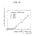
- Fig. 14 illustrates the relationship between the amount of change of the stress and the amount that the crystal structure changed. Plotted on a vertical axis is the X-ray diffraction peak strength ratio of the (111) orientation of the gold plated film to the (200) orientation thereof. The amount of change of the stress during an annealing time is plotted on a horizontal axis.
- the change in the amount of the stress of a gold plated film during aging and heat treatment thereof is not related to the release of elements or absorption of elements due to any reaction, as has been believed thus far, but occurs only due to the force relationship between the film and the substrate. Also, heat was not a direct cause of the stress change.
- the amount of stress of the gold plated film is changed easily by an outside stress and thus the crystal structure thereof changes.
- the change of the crystal structure of the gold plated film is not caused by heat only.
- the stress reduction due to heat treatment occurs during the change from the (111) to the (200) orientation. Since this change occurs nonuniformly within the film, a large positional deviation occurs in local regions where the change amount is small. This means that a local positional deviation can be suppressed if the (111) orientation is changed to the (200) orientation by an amount sufficient enough to reduce (111) orientation and the change is distributed uniformly within the film even if the local positional deviation exists.
- the present invention uses an absorber in which the crystal orientation is made uniform within the film.
- an X-ray absorber is heated and cooled repeatedly in order to change the film of the (111) orientation until the X-ray absorber is sufficiently changed to the (200) crystal orientation, thereby eliminating the orientation nonuniformity and a local positional deviations in the X-ray absorber.
- the temperature is too high, gold is diffused within the substrate, while, if it is too low, the heating operation takes a long time. Thus, a temperature ranging from 30 to 300°C should be used. In contrast, the cooling operation should be performed at a temperature lower than the heating temperature. However, if the temperature is too high, the number of times the operation has to be repeated becomes large since the amount of the change of the crystal structure is small. Thus, preferably a temperature lower than 0°C should be used. Any heating device can be used for the annealing operation, but usually, a hot plate, an oven or the like is used.
- gas such as nitrogen or argon
- a solvent such as alcohol or acetone
- the use of liquefied nitrogen enables the cooling time to be shortened considerably.
- the line expansion coefficient of a substrate on which the X-ray absorber is formed be one half of or less than that of the X-ray absorber.
- manufacturing steps other than the above-mentioned step of manufacturing X-ray absorbers for example, the step of forming X-ray permeable films or the step of producing holding frames, which are well known, are performed.
- the X-ray permeable film is preferably formed to a thickness between 1 and 10 ⁇ m to reduce the deviation between the designed line width and a transfer line width as much as possible.
- the X-ray permeable film is formed from well-known materials, such as inorganic films made of Si, SiO 2 , SiC, SiN, SiCN, BN, or BNC, or radiation resistant organic films, such as polyimide.
- the X-ray absorber which absorbs X-rays is usually formed to a thickness of 0.2 to 1.0 ⁇ m.
- the frame for supporting an X-ray permeable film is formed by a silicon wafer or the like. Moreover, a holding frame for assisting the transport of a mask substrate may be provided on the supporting frame.
- This supporting frame is formed from materials of heat resistant glass, Ti, an Fe-Co alloy, ceramics, or the like.
- a film for protecting an X-ray absorber, an electroconductive film, a film for preventing alignment light from being reflected or the like may be provided on the X-ray mask structure of the present invention.
- the present invention has a feature in that the X-ray exposure method and the device of the present invention uses an X-ray mask structure having the above-described structure.
- the X-ray exposure method of the present invention comprises the step of transferring X-ray absorber patterns to a member to be transferred by exposing the member to be transferred with X-rays via the X-ray mask structure.
- the device of the present invention is manufactured by exposing a substrate to be processed with X-rays via the X-ray mask structure to transfer an X-ray absorber pattern to the substrate to be processed and by processing and fabricating the substrate.
- the X-ray exposure of the present invention may be a conventional, well-known method except that the X-ray mask structure of the present invention is used.
- the device of the present invention is a device manufactured by a conventional, well-known method except that the X-ray mask structure of the present invention is used.
- a silicon nitride film was formed to a thickness of 2 ⁇ m on an Si substrate having a thickness of 2 mm by a CVD method.
- the silicon nitride film on the reverse surface thereof was etched to a predetermined shape by a dry etching process.
- Si was etched by a potassium hydroxide solution with the silicon nitride film on the reverse surface as a mask to open a window.
- the gold plated film was a (111) crystal oriented film having an internal stress of -5E+0.8N/m 2 (8 dyn/cm 2 ) (compressive stress).
- the resist was peeled off, thus forming an X-ray mask.
- the X-ray mask was heated at 120°C for one hour. After it was cooled to room temperature, an X-ray diffraction test was carried out. The results of the test showed that the gold plated film has an internal stress of +10E+0.8N/m 2 (8 dyn/cm 2 ) (tensile stress) and the (111) was 2.5 with respect to the peak strength 1 of the (200) regarding the crystal orientation of the gold-plated film.
- the X-ray mask was cooled in liquefied nitrogen for one hour. After it is heated to room temperature, an X-ray diffraction test was carried out. The results of the test showed that the gold-plated film has an internal stress of -2E+0.8N/m 2 (8 dyn/cm 2 ) and the (111) was 1.1 with respect to the peak strength 1 of the (200) orientation regarding the crystal orientation of the gold-plated film.
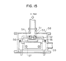
- Fig. 15 is a simplified illustration of the X-ray exposure apparatus.
- Reference numeral 8 denotes an exposure chamber;
- reference numeral 1 denotes a beryllium (Be) port;
- reference numeral 9 denotes an exhaust port.
- the exposure chamber 8 is shut off from an X-ray generation source by Be. Exposure is possible inside the chamber when the inside thereof contains any of the following: air, a vacuum, He atmosphere or the like.
- Reference numeral 52 denotes a mask stage
- reference numeral 53 denotes an alignment detection section
- reference numeral 54 denotes an X-ray mask structure
- reference numeral 55 denotes a wafer (semiconductor substrate)
- reference numeral 56 denotes a wafer chuck
- reference numeral 57 denotes a wafer stage.
- the X-ray mask structure 54 is mechanically set in a direction predetermined to some degree by using a positioning pin, orientation flat or the like when the X-ray mask structure 54 is attached to the mask stage 52.
- the wafer 55 is set in the wafer chuck 56 in a similar manner.
- the relative positional relationship between the X-ray mask structure 54 and the wafer 55 is determined by an instruction from the alignment detection section 53. Thereafter, they are exposed by X-rays.
- the positional deviation of the pattern was less than 0.03 ⁇ m, which is the measurement accuracy of the apparatus, and a high-accuracy semiconductor device could be manufactured.
- the X-ray absorber was heated and cooled repeatedly in a mask used for X-ray exposure, the mask being formed of an X-ray absorber, an X-ray permeable film and a member for supporting the X-ray permeable film, so that the crystal orientation of the X-ray absorber is changed from (111) orientation to (200) as claimed in claim 1.
- a pattern having a small amount of positional deviations could be formed.
Landscapes
- Physics & Mathematics (AREA)
- General Physics & Mathematics (AREA)
- Preparing Plates And Mask In Photomechanical Process (AREA)
- Exposure Of Semiconductors, Excluding Electron Or Ion Beam Exposure (AREA)
- Electroplating And Plating Baths Therefor (AREA)
- Drying Of Semiconductors (AREA)
- Formation Of Insulating Films (AREA)
Claims (11)
- Structure de masquage de rayons X comprenant un absorbeur de rayons X, un film perméable aux rayons X et un châssis destiné à supporter le film perméable aux rayons X, dans lequel l'absorbeur de rayons X est constitué d'or,
caractérisé en ce que :
ledit absorbeur de rayons X a une orientation de cristaux ayant un rapport (111)/(200) d'intensité de crête de diffraction de rayons X de moins de 0,5. - Structure de masquage de rayons X selon la revendication 1, dans laquelle le coefficient d'allongement longitudinal du film perméable aux rayons X est d'un demi de celui de l'absorbeur de rayons X.
- Structure de masquage de rayons X selon la revendication 1 ou 2, dans laquelle le rapport (111)/(200) d'intensité de crête de diffraction de rayons X est de moins de 0,35.
- Structure de masquage de rayons X selon l'une quelconque des revendications 1 à 3, dans laquelle le film perméable aux rayons X est un film en nitrure de silicium.
- Structure de masquage de rayons X selon l'une quelconque des revendications 1 à 4, dans laquelle l'épaisseur du film perméable aux rayons X se situe entre 1 µm et 10 µm, et l'épaisseur de l'absorbeur de rayons X se situe entre 0,2 µm et 10 µm.
- Procédé d'exposition aux rayons X en utilisant une structure de masquage de rayons X selon l'une quelconque des revendications 1 à 5, comprenant :le fait d'exposer un élément à des rayons X à travers ladite structure de masquage de rayons X ; etle fait de transférer le motif dudit absorbeur de rayons X vers ledit élément.
- Procédé de fabrication d'une structure de masquage de rayons X selon l'une quelconque des revendications 1 à 5, comprenant :la formation d'un film perméable aux rayons X sur un châssis ;la formation d'un absorbeur de rayons X constitué d'un film d'or sur ledit film perméable aux rayons X ; etle chauffage et le refroidissement une pluralité de fois dudit absorbeur de rayons X, dans lequel on répète une pluralité de fois lesdites étapes de chauffage et de refroidissement jusqu'à ce que le film d'or ait une orientation de cristaux ayant un rapport (111)/(200) d'intensité de crête de diffraction de rayons X de moins de 0,5.
- Procédé de fabrication d'une structure de masquage de rayons X selon la revendication 7, dans lequel le film d'or est formé par placage.
- Procédé de fabrication d'une structure de masquage de rayons X selon la revendication 8 ou 9, dans lequel on répète une pluralité de fois lesdites étapes de chauffage et de refroidissement jusqu'à ce que l'orientation (200) du film d'or atteigne sa saturation.
- Procédé de fabrication d'une structure de masquage de rayons X selon l'une quelconque des revendications 7 à 9, dans lequel on effectue ledit chauffage à une température située entre 30 et 300°C.
- Procédé de fabrication d'une structure de masquage de rayons X selon l'une quelconque des revendications 7 à 10, dans lequel on effectue ledit refroidissement à une température située au-dessous de 0°C.
Applications Claiming Priority (3)
| Application Number | Priority Date | Filing Date | Title |
|---|---|---|---|
| JP28409491A JP3073067B2 (ja) | 1991-10-04 | 1991-10-04 | X線露光用マスク及びその製造方法 |
| JP28409491 | 1991-10-04 | ||
| JP284094/91 | 1991-10-04 |
Publications (2)
| Publication Number | Publication Date |
|---|---|
| EP0536635A1 EP0536635A1 (fr) | 1993-04-14 |
| EP0536635B1 true EP0536635B1 (fr) | 1999-06-16 |
Family
ID=17674143
Family Applications (1)
| Application Number | Title | Priority Date | Filing Date |
|---|---|---|---|
| EP92116781A Expired - Lifetime EP0536635B1 (fr) | 1991-10-04 | 1992-09-30 | Masque à rayons X, méthode de fabrication et d'exposition |
Country Status (6)
| Country | Link |
|---|---|
| US (1) | US5247557A (fr) |
| EP (1) | EP0536635B1 (fr) |
| JP (1) | JP3073067B2 (fr) |
| AT (1) | ATE181427T1 (fr) |
| CA (1) | CA2079725C (fr) |
| DE (1) | DE69229430T2 (fr) |
Families Citing this family (5)
| Publication number | Priority date | Publication date | Assignee | Title |
|---|---|---|---|---|
| SG43954A1 (en) * | 1991-11-15 | 1997-11-14 | Canon Kk | X-ray mask structure and x-ray exposing method and semiconductor device manufactured by use of x-ray mask structure and method for manufacturing x-ray mask structure |
| JPH07117605B2 (ja) * | 1992-03-13 | 1995-12-18 | 日本ピラー工業株式会社 | 回折格子 |
| US5318687A (en) * | 1992-08-07 | 1994-06-07 | International Business Machines Corporation | Low stress electrodeposition of gold for X-ray mask fabrication |
| ZA94614B (en) * | 1993-02-11 | 1994-08-12 | Sasol Chem Ind Pty | Solvent extraction |
| JP3586031B2 (ja) * | 1996-03-27 | 2004-11-10 | 株式会社東芝 | サセプタおよび熱処理装置および熱処理方法 |
Family Cites Families (3)
| Publication number | Priority date | Publication date | Assignee | Title |
|---|---|---|---|---|
| JPS5760839A (en) * | 1980-09-30 | 1982-04-13 | Nec Corp | Manufacture of x-ray exposure mask |
| JPH0715880B2 (ja) * | 1989-12-26 | 1995-02-22 | 信越化学工業株式会社 | X線リソグラフィー用SiC膜、その製造方法およびX線リソグラフィー用マスク |
| US5124561A (en) * | 1991-04-04 | 1992-06-23 | International Business Machines Corporation | Process for X-ray mask warpage reduction |
-
1991
- 1991-10-04 JP JP28409491A patent/JP3073067B2/ja not_active Expired - Fee Related
-
1992
- 1992-09-30 DE DE69229430T patent/DE69229430T2/de not_active Expired - Fee Related
- 1992-09-30 AT AT92116781T patent/ATE181427T1/de not_active IP Right Cessation
- 1992-09-30 EP EP92116781A patent/EP0536635B1/fr not_active Expired - Lifetime
- 1992-10-01 US US07/955,266 patent/US5247557A/en not_active Expired - Fee Related
- 1992-10-02 CA CA002079725A patent/CA2079725C/fr not_active Expired - Fee Related
Also Published As
| Publication number | Publication date |
|---|---|
| CA2079725A1 (fr) | 1993-04-05 |
| DE69229430D1 (de) | 1999-07-22 |
| US5247557A (en) | 1993-09-21 |
| DE69229430T2 (de) | 1999-12-23 |
| EP0536635A1 (fr) | 1993-04-14 |
| CA2079725C (fr) | 1998-02-03 |
| JPH05102012A (ja) | 1993-04-23 |
| JP3073067B2 (ja) | 2000-08-07 |
| ATE181427T1 (de) | 1999-07-15 |
Similar Documents
| Publication | Publication Date | Title |
|---|---|---|
| US6096661A (en) | Method for depositing silicon dioxide using low temperatures | |
| US6140255A (en) | Method for depositing silicon nitride using low temperatures | |
| JPH0317369B2 (fr) | ||
| JPH03114049A (ja) | シリコンシャドウマスク形成方法 | |
| US4370556A (en) | Self-supporting mask, method for production as well as use of same | |
| US4994141A (en) | Method of manufacturing a mask support of SiC for radiation lithography masks | |
| EP0536635B1 (fr) | Masque à rayons X, méthode de fabrication et d'exposition | |
| KR20220006887A (ko) | 극자외선 리소그라피용 펠리클의 제조방법 | |
| US5375157A (en) | X-ray mask structure and a production method thereof, an exposure method using the X-ray mask structure, and a device fabricated by using the X-ray mask structure | |
| US5567551A (en) | Method for preparation of mask for ion beam lithography | |
| US6514877B1 (en) | Method using sub-micron silicide structures formed by direct-write electron beam lithography for fabricating masks for extreme ultra-violet and deep ultra-violet lithography | |
| US7867403B2 (en) | Temperature control method for photolithographic substrate | |
| KR100211012B1 (ko) | 리소그래픽마스크구조체와 그 생산방법 및 디바이스제조방법 | |
| JP3626284B2 (ja) | マスク基板の熱処理方法とその装置 | |
| US5335256A (en) | Semiconductor substrate including a single or multi-layer film having different densities in the thickness direction | |
| Noguchi et al. | Fabrication of x-ray mask from a diamond membrane and its evaluation | |
| JP3056538B2 (ja) | 等倍転写用x線マスクの製造方法 | |
| Shimkunas et al. | Mask technology for x-ray step-and-repeat system | |
| US6190808B1 (en) | X-ray mask and method of manufacturing the same | |
| Tsuboi et al. | High synchrotron radiation durability microwave plasma chemical vapor deposition diamond x‐ray mask membrane | |
| JPH07201706A (ja) | 半導体装置の製造方法、x線マスク構造体の製造方法、x線マスク構造体、該x線マスク構造体を用いたx線露光方法及びx線露光装置、該x線露光方法を適用して製造される半導体装置 | |
| JP3279181B2 (ja) | X線露光用マスクの製造方法 | |
| Ezaki et al. | Critical-dimension controllability of chemically amplified resists for X-ray membrane mask fabrication | |
| JP2001185479A (ja) | リソグラフィ用マスク基板およびその製造方法 | |
| Sen et al. | Low distortion, large area ion beam proximity printing for GaAs field effect transistors and monolithic microwave integrated circuits |
Legal Events
| Date | Code | Title | Description |
|---|---|---|---|
| PUAI | Public reference made under article 153(3) epc to a published international application that has entered the european phase |
Free format text: ORIGINAL CODE: 0009012 |
|
| AK | Designated contracting states |
Kind code of ref document: A1 Designated state(s): AT BE CH DE DK ES FR GB GR IT LI LU NL PT SE |
|
| 17P | Request for examination filed |
Effective date: 19930928 |
|
| 17Q | First examination report despatched |
Effective date: 19961213 |
|
| GRAG | Despatch of communication of intention to grant |
Free format text: ORIGINAL CODE: EPIDOS AGRA |
|
| GRAG | Despatch of communication of intention to grant |
Free format text: ORIGINAL CODE: EPIDOS AGRA |
|
| GRAH | Despatch of communication of intention to grant a patent |
Free format text: ORIGINAL CODE: EPIDOS IGRA |
|
| GRAH | Despatch of communication of intention to grant a patent |
Free format text: ORIGINAL CODE: EPIDOS IGRA |
|
| GRAH | Despatch of communication of intention to grant a patent |
Free format text: ORIGINAL CODE: EPIDOS IGRA |
|
| GRAA | (expected) grant |
Free format text: ORIGINAL CODE: 0009210 |
|
| AK | Designated contracting states |
Kind code of ref document: B1 Designated state(s): AT BE CH DE DK ES FR GB GR IT LI LU NL PT SE |
|
| PG25 | Lapsed in a contracting state [announced via postgrant information from national office to epo] |
Ref country code: IT Free format text: LAPSE BECAUSE OF FAILURE TO SUBMIT A TRANSLATION OF THE DESCRIPTION OR TO PAY THE FEE WITHIN THE PRESCRIBED TIME-LIMIT;WARNING: LAPSES OF ITALIAN PATENTS WITH EFFECTIVE DATE BEFORE 2007 MAY HAVE OCCURRED AT ANY TIME BEFORE 2007. THE CORRECT EFFECTIVE DATE MAY BE DIFFERENT FROM THE ONE RECORDED. Effective date: 19990616 Ref country code: ES Free format text: THE PATENT HAS BEEN ANNULLED BY A DECISION OF A NATIONAL AUTHORITY Effective date: 19990616 Ref country code: CH Free format text: LAPSE BECAUSE OF FAILURE TO SUBMIT A TRANSLATION OF THE DESCRIPTION OR TO PAY THE FEE WITHIN THE PRESCRIBED TIME-LIMIT Effective date: 19990616 Ref country code: BE Free format text: LAPSE BECAUSE OF FAILURE TO SUBMIT A TRANSLATION OF THE DESCRIPTION OR TO PAY THE FEE WITHIN THE PRESCRIBED TIME-LIMIT Effective date: 19990616 Ref country code: AT Free format text: LAPSE BECAUSE OF FAILURE TO SUBMIT A TRANSLATION OF THE DESCRIPTION OR TO PAY THE FEE WITHIN THE PRESCRIBED TIME-LIMIT Effective date: 19990616 Ref country code: GR Free format text: LAPSE BECAUSE OF NON-PAYMENT OF DUE FEES Effective date: 19990616 Ref country code: LI Free format text: LAPSE BECAUSE OF FAILURE TO SUBMIT A TRANSLATION OF THE DESCRIPTION OR TO PAY THE FEE WITHIN THE PRESCRIBED TIME-LIMIT Effective date: 19990616 Ref country code: SE Free format text: THE PATENT HAS BEEN ANNULLED BY A DECISION OF A NATIONAL AUTHORITY Effective date: 19990616 Ref country code: NL Free format text: LAPSE BECAUSE OF FAILURE TO SUBMIT A TRANSLATION OF THE DESCRIPTION OR TO PAY THE FEE WITHIN THE PRESCRIBED TIME-LIMIT Effective date: 19990616 |
|
| REF | Corresponds to: |
Ref document number: 181427 Country of ref document: AT Date of ref document: 19990715 Kind code of ref document: T |
|
| REG | Reference to a national code |
Ref country code: CH Ref legal event code: EP |
|
| REF | Corresponds to: |
Ref document number: 69229430 Country of ref document: DE Date of ref document: 19990722 |
|
| ET | Fr: translation filed | ||
| PG25 | Lapsed in a contracting state [announced via postgrant information from national office to epo] |
Ref country code: DK Free format text: LAPSE BECAUSE OF FAILURE TO SUBMIT A TRANSLATION OF THE DESCRIPTION OR TO PAY THE FEE WITHIN THE PRESCRIBED TIME-LIMIT Effective date: 19990916 Ref country code: PT Free format text: LAPSE BECAUSE OF FAILURE TO SUBMIT A TRANSLATION OF THE DESCRIPTION OR TO PAY THE FEE WITHIN THE PRESCRIBED TIME-LIMIT Effective date: 19990916 |
|
| PG25 | Lapsed in a contracting state [announced via postgrant information from national office to epo] |
Ref country code: LU Free format text: LAPSE BECAUSE OF NON-PAYMENT OF DUE FEES Effective date: 19990930 |
|
| NLV1 | Nl: lapsed or annulled due to failure to fulfill the requirements of art. 29p and 29m of the patents act | ||
| REG | Reference to a national code |
Ref country code: CH Ref legal event code: PL |
|
| PLBE | No opposition filed within time limit |
Free format text: ORIGINAL CODE: 0009261 |
|
| 26N | No opposition filed | ||
| REG | Reference to a national code |
Ref country code: GB Ref legal event code: IF02 |
|
| PGFP | Annual fee paid to national office [announced via postgrant information from national office to epo] |
Ref country code: FR Payment date: 20020910 Year of fee payment: 11 |
|
| PGFP | Annual fee paid to national office [announced via postgrant information from national office to epo] |
Ref country code: GB Payment date: 20020925 Year of fee payment: 11 |
|
| PGFP | Annual fee paid to national office [announced via postgrant information from national office to epo] |
Ref country code: DE Payment date: 20021011 Year of fee payment: 11 |
|
| PG25 | Lapsed in a contracting state [announced via postgrant information from national office to epo] |
Ref country code: GB Free format text: LAPSE BECAUSE OF NON-PAYMENT OF DUE FEES Effective date: 20030930 |
|
| PG25 | Lapsed in a contracting state [announced via postgrant information from national office to epo] |
Ref country code: DE Free format text: LAPSE BECAUSE OF NON-PAYMENT OF DUE FEES Effective date: 20040401 |
|
| GBPC | Gb: european patent ceased through non-payment of renewal fee |
Effective date: 20030930 |
|
| PG25 | Lapsed in a contracting state [announced via postgrant information from national office to epo] |
Ref country code: FR Free format text: LAPSE BECAUSE OF NON-PAYMENT OF DUE FEES Effective date: 20040528 |
|
| REG | Reference to a national code |
Ref country code: FR Ref legal event code: ST |