EP0534638A1 - Système d'ajustage de la phase d'horloge à faible instabilité - Google Patents
Système d'ajustage de la phase d'horloge à faible instabilité Download PDFInfo
- Publication number
- EP0534638A1 EP0534638A1 EP92308184A EP92308184A EP0534638A1 EP 0534638 A1 EP0534638 A1 EP 0534638A1 EP 92308184 A EP92308184 A EP 92308184A EP 92308184 A EP92308184 A EP 92308184A EP 0534638 A1 EP0534638 A1 EP 0534638A1
- Authority
- EP
- European Patent Office
- Prior art keywords
- sinewave
- input
- signals
- phase
- coupled
- Prior art date
- Legal status (The legal status is an assumption and is not a legal conclusion. Google has not performed a legal analysis and makes no representation as to the accuracy of the status listed.)
- Granted
Links
Images


Classifications
-
- H—ELECTRICITY
- H03—ELECTRONIC CIRCUITRY
- H03K—PULSE TECHNIQUE
- H03K17/00—Electronic switching or gating, i.e. not by contact-making and –breaking
- H03K17/51—Electronic switching or gating, i.e. not by contact-making and –breaking characterised by the components used
- H03K17/56—Electronic switching or gating, i.e. not by contact-making and –breaking characterised by the components used by the use, as active elements, of semiconductor devices
- H03K17/60—Electronic switching or gating, i.e. not by contact-making and –breaking characterised by the components used by the use, as active elements, of semiconductor devices the devices being bipolar transistors
- H03K17/62—Switching arrangements with several input- output-terminals, e.g. multiplexers, distributors
- H03K17/6257—Switching arrangements with several input- output-terminals, e.g. multiplexers, distributors with several inputs only combined with selecting means
- H03K17/6264—Switching arrangements with several input- output-terminals, e.g. multiplexers, distributors with several inputs only combined with selecting means using current steering means
Definitions
- the present invention relates to clock delay circuits, and more particularly to a low jitter clock phase adjust system for continuously varying the phase of a sinusoidal clock signal over a range of greater than three hundred sixty degrees (360°).
- test instruments such as oscilloscopes, derive all timing information from a master clock.
- An example of an extremely stable master clock is a surface acoustic wave (SAW) oscillator that is capable of generating a sine wave at a high frequency.
- SAW surface acoustic wave
- the RC network includes a variable resistor that alters the slope of the input clock pulses, and hence the point at which the comparator switches from a high state to a low state.
- the effect of this circuit is that, as the slope flattens out, the phase of the output pulses becomes retarded in time with respect to the input pulses because the comparator is triggered at a later time during each cycle.
- the input to the comparator frequently includes jitter and high frequency noise that causes uncertainty as to the time when the input pulse edges encounter the threshold of the comparator. The result is jitter in the output pulses.
- the four-quadrant multipliers used by Lamb are noisy when operated in midrange, i.e., when balanced. Even when the multipliers are balanced so that there is no contribution to the sum from one quadrature component, such noise causes some jitter in the output signal. Further without additional compensation circuitry the amplitude of the output of the summation circuit varies from one, where only one quadrature component contributes to the output, to 1.4, a forty percent amplitude change, when both quadrature components contribute equally to the output. Also the fact that the four-quadrant multipliers tie the collectors together introduces additional capacitance in the circuit, which may require a common base stage at the summing nodes at the outputs of the multipliers. This additional amplification stage may in turn require a larger power supply with the attendant greater power usage.
- What is desired is a low jitter clock phase adjust system that reduces the noise due to the use of multipliers, reduces the circuit capacitance, provides a more constant amplitude output and requires a lower voltage power supply for reduced power usage.
- the present invention provides a low jitter clock phase adjust system that divides an input clock signal into three components one hundred twenty degrees (120°) out of phase with each other.
- the three clock components are input to a trio of two-quadrant multipliers configured such that only one multiplier at a time is in transition at any given time or phase angle.
- a control circuit converts an input control voltage into control currents for the multipliers to provide an essentially linear variation over a greater than three hundred sixty degree (360°) range.
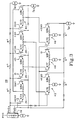
- Fig. 1 is a block diagram of a low jitter clock phase adjust system according to the present invention.
- Fig. 2 is a partial schematic diagram of the multiplier portion of the low jitter clock phase adjust system of Fig. 1.
- Fig. 3 is a partial schematic diagram of the control portion of the low jitter clock phase adjust system of Fig. 1.
- Figs. 4A and 4B are graphs illustrating in vector form the phase adjustment according to the present invention.
- Fig. 5 is a graph of the control currents for the multipliers used in the present invention.
- Fig. 6 is a graph illustrating the linearity of the low jitter clock phase adjust system of the present invention.
- an oscillator 10 such as an extremely stable SAW oscillator, is divided into three phases PH1, PH2 and PH3 by appropriate precision delay elements 12, 14.
- the three phases are separated from each other by one hundred twenty degrees (120°).
- the precision delay elements 12, 14 may be different length strip line structures, as is well known in the art, for a fixed sinewave output from the oscillator 10.
- the three phases PH1, PH2 and PH3 are input to respective voltage to current converters 16, 18, 20 to produce three differential current vectors I1, I2, I3 having phases at zero, 120 and 240 degrees relative to each other.
- the three current vectors I1, I2, I3 are input to a trio of two-quadrant multipliers 22, 24, 26 with currents I1 and nI1 being input to the first multiplier, currents I2 and nI2 being input to the second multiplier, and currents I3 and nI3 being input to the third multiplier, "n" indicating a "not” function.
- a control circuit 28 in response to a phase control signal PHS provides three control currents i0, i120, i240 that are applied to the respective multipliers.
- the outputs of the multipliers 22, 24, 26 are summed, typically at a summing node 30, to produce a low jitter phase adjusted clock signal output.
- multipliers 22, 24, 26 are in a transitional state while another is fully ON and the other is fully OFF. Since multipliers produce the most noise when operating in their linear range and the least noise when either fully ON or OFF, then with only one multiplier transitioning the least noise is produced.
- Each two-quadrant multiplier 22, 24, 26 has two pairs of transistors Q1, Q2; Q3, Q4 with the bases being cross-coupled, such that the base of Q1 is coupled to the base of Q4 and the base of Q2 is coupled to the base of Q3.
- the bases also are coupled to a bias current source Ib.
- the collectors of Q1 and Q4 are coupled to the summing node 30 and to load resistors R2, R3.
- the collectors of Q2 and Q3 are coupled to around.
- the control currents i0, i120, i240 are coupled between the bases of Q1 and Q2.
- Each voltage-to-current converter 16, 18, 20 has a pair of emitter coupled transistors Q5, Q6 with adjacent phases of the clock signal applied to the bases, i.e., PH1 and PH2 are applied to the bases of Q5A and Q6A respectively, etc.
- the emitters are resistively coupled via resistors R1 with individual current sources coupled to each emitter.
- the collectors of the transistors Q5, Q6 are coupled to the emitter junctions of the transistor pairs Q1, Q2; Q3, Q4 to provide current to the multipliers 22, 24, 26.
- signals PH1, PH2, PH3 applied to the bases of transistors Q5, Q6 of the voltage-to-current converters 16, 18, 20 are shown as adjacent clock phase signals, either the base of Q5 or the base of Q6 may be connected to a reference bias voltage so that only one clock phase signal is input to each voltage-to-current converter.
- the controller circuit 28 has a conventional input converter 32 that converts the single-ended voltage phase control signal PHS to a differential phase control signal PHS+, PHS-.
- a plurality of current switches 34-46, each having a pair of emitter coupled transistors Q7, Q8, are coupled to receive the PHS+ and PHS- signals.
- Current switch 34 is coupled directly between the PHS+ and PHS-signals at the bases of Q7A and Q8A.
- PHS- is coupled directly to the base of transistor Q8 in each of current switches 36, 38 and by a junction drop to the base of transistor Q8D.
- PHS+ is coupled directly to the bases of transistor Q7 in each of current switches 42, 44, 46.
- a resistor ladder of series resistors R+ couples PHS+ to the bases of transistors Q7 in each of the current switches 36, 38, 40.
- a resistor ladder of series resistors R- couples PHS- to the bases of transistors Q8 in each of the current switches 42, 44, 46.
- Current sources Ib1, Ib2 supply current to the resistor ladders R+, R-.
- the output of current switch 34 is the i240 control signal
- the output of current switch 36 is the i0 control signal
- the output of current switch 38 is the i120 control signal.
- the collector of transistor Q7D of current switch 40 is wire ORed with the i240 output of current switch 34, and the collector of transistor Q8D is coupled as a current source for current switch 34.
- collector of Q7E is coupled as a current source for current switch 38 and the collector of Q8E is wire ORed with the ni120 output of current switch 38
- collector of Q7F is coupled as a current source for current switch 36 and the collector of Q8F is wire ORed with the i0 output of current switch 36
- collector of Q7G is coupled as a current source for current switch 40 and the collector of Q8G is wire ORed with the ni240 output of current switch 34.
- Each of current switches 42, 44, 46 has a fixed current source coupled to the emitters.
- the voltage-to-current converters 16, 18, 20 provide three current vectors I1, I2, I3 that are 120° out of phase with each other.
- the multipliers 22, 24, 26 multiply the three current vectors, represented by PH1, PH2, PH3 by the appropriate phase control signal i0, i120, i240 and the resulting scaled vectors are summed.
- the resulting clock output has a resultant phase of 30° with an amplitude of 0.866, a less than fifteen percent amplitude variation.
- the resultant phase of the clock output is 60° with an amplitude equal to unity.
- Fig. 5 illustrates the characteristics of the control circuit 28 in response to the control current PHS. The transitions for each current i0, i120 and i240 occur while the other two currents are constant, either on or off. Thus only one current changes at any given instant.
- transistor Q8D gradually turns on, gradually supplying current to transistor Q7A, while transistor Q7D is gradually being turned off. This results in the transition from i240 to ni240 while i0 is constant and ni120 is constant.
- the clock delay is virtually a linear function of the control voltage.
- the dotted line is the slope of the solid line, showing the non-linearity of the phase control function. Ideally the dotted line would be a horizontal line.
- the present invention provides a low jitter phase adjust scheme for a clock that has a greater than 360° adjustment range by dividing the input clock signal into three phases, and using two-quadrant multipliers so that only one phase control current varies at a time.
Landscapes
- Stabilization Of Oscillater, Synchronisation, Frequency Synthesizers (AREA)
- Pulse Circuits (AREA)
Applications Claiming Priority (2)
| Application Number | Priority Date | Filing Date | Title |
|---|---|---|---|
| US765785 | 1991-09-26 | ||
| US07/765,785 US5157276A (en) | 1991-09-26 | 1991-09-26 | Low jitter clock phase adjust system |
Publications (2)
| Publication Number | Publication Date |
|---|---|
| EP0534638A1 true EP0534638A1 (fr) | 1993-03-31 |
| EP0534638B1 EP0534638B1 (fr) | 1996-11-06 |
Family
ID=25074477
Family Applications (1)
| Application Number | Title | Priority Date | Filing Date |
|---|---|---|---|
| EP92308184A Expired - Lifetime EP0534638B1 (fr) | 1991-09-26 | 1992-09-09 | Système d'ajustage de la phase d'horloge à faible instabilité |
Country Status (4)
| Country | Link |
|---|---|
| US (1) | US5157276A (fr) |
| EP (1) | EP0534638B1 (fr) |
| JP (1) | JPH05199089A (fr) |
| DE (1) | DE69215054D1 (fr) |
Families Citing this family (14)
| Publication number | Priority date | Publication date | Assignee | Title |
|---|---|---|---|---|
| US5402019A (en) * | 1992-08-06 | 1995-03-28 | Tektronix, Inc. | Phase startable clock device |
| KR100393317B1 (ko) * | 1994-02-15 | 2003-10-23 | 람버스 인코포레이티드 | 지연동기루프 |
| US5554945A (en) * | 1994-02-15 | 1996-09-10 | Rambus, Inc. | Voltage controlled phase shifter with unlimited range |
| US6009039A (en) * | 1994-02-17 | 1999-12-28 | Fujitsu Limited | Semiconductor device |
| KR0158762B1 (ko) * | 1994-02-17 | 1998-12-01 | 세키자와 다다시 | 반도체 장치 |
| WO1996037952A1 (fr) | 1995-05-26 | 1996-11-28 | Rambus, Inc. | Dephaseur a usage dans un generateur de signal d'horloge en quadrature |
| FR2736776B1 (fr) * | 1995-07-13 | 1997-09-26 | Sgs Thomson Microelectronics | Synthetiseur de frequences |
| US6404255B1 (en) * | 1995-09-22 | 2002-06-11 | Thomson Licensing S.A. | Phase shift apparatus |
| US5945860A (en) * | 1996-01-04 | 1999-08-31 | Northern Telecom Limited | CLM/ECL clock phase shifter with CMOS digital control |
| US6247138B1 (en) * | 1997-06-12 | 2001-06-12 | Fujitsu Limited | Timing signal generating circuit, semiconductor integrated circuit device and semiconductor integrated circuit system to which the timing signal generating circuit is applied, and signal transmission system |
| TW440767B (en) | 1998-06-02 | 2001-06-16 | Fujitsu Ltd | Method of and apparatus for correctly transmitting signals at high speed without waveform distortion |
| TW483255B (en) * | 1999-11-26 | 2002-04-11 | Fujitsu Ltd | Phase-combining circuit and timing signal generator circuit for carrying out a high-speed signal transmission |
| US20050084047A1 (en) * | 2003-09-30 | 2005-04-21 | Seiko Epson Corporation | Clock signal correcting circuit and communicating apparatus |
| US20060062340A1 (en) * | 2004-09-20 | 2006-03-23 | Intersil Americas, Inc. | Phase adjuster |
Citations (1)
| Publication number | Priority date | Publication date | Assignee | Title |
|---|---|---|---|---|
| US4808936A (en) * | 1988-03-25 | 1989-02-28 | Tektronix, Inc. | Continuously variable clock delay circuit |
Family Cites Families (5)
| Publication number | Priority date | Publication date | Assignee | Title |
|---|---|---|---|---|
| JPS5910621B2 (ja) * | 1975-01-08 | 1984-03-10 | 日本電気株式会社 | デ−タ伝送復調器 |
| US3978407A (en) * | 1975-07-23 | 1976-08-31 | Codex Corporation | Fast start-up adaptive equalizer communication system using two data transmission rates |
| CA1268523A (fr) * | 1984-10-31 | 1990-05-01 | Nec Corporation | Circuit de synchronisation pouvant etablir le synchronisme meme lorsque la frequence d'echantillonnage est invariable |
| US4868428A (en) * | 1987-02-20 | 1989-09-19 | Cooper J Carl | Apparatus for shifting the frequency of complex signals |
| US4797586A (en) * | 1987-11-25 | 1989-01-10 | Tektronix, Inc. | Controllable delay circuit |
-
1991
- 1991-09-26 US US07/765,785 patent/US5157276A/en not_active Expired - Lifetime
-
1992
- 1992-09-09 DE DE69215054T patent/DE69215054D1/de not_active Expired - Lifetime
- 1992-09-09 EP EP92308184A patent/EP0534638B1/fr not_active Expired - Lifetime
- 1992-09-25 JP JP4281018A patent/JPH05199089A/ja active Pending
Patent Citations (1)
| Publication number | Priority date | Publication date | Assignee | Title |
|---|---|---|---|---|
| US4808936A (en) * | 1988-03-25 | 1989-02-28 | Tektronix, Inc. | Continuously variable clock delay circuit |
Non-Patent Citations (1)
| Title |
|---|
| 15th EUROP. MICROW. CONF.; 9-13/9/85;PARIS (FR); W.MIELKE: AN ACTIVE PHASE SHIFTER FOR PHASED ARRAY APPLICATIONS PROVIDING AMPLITUDE AND PHASE CONTROL; P572-577 * |
Also Published As
| Publication number | Publication date |
|---|---|
| US5157276A (en) | 1992-10-20 |
| JPH05199089A (ja) | 1993-08-06 |
| EP0534638B1 (fr) | 1996-11-06 |
| DE69215054D1 (de) | 1996-12-12 |
Similar Documents
| Publication | Publication Date | Title |
|---|---|---|
| US5157276A (en) | Low jitter clock phase adjust system | |
| US4638255A (en) | Rectangular wave pulse generators | |
| US4843339A (en) | Isolation amplifier including precision voltage-to-duty-cycle converter and low ripple, high bandwidth charge balance demodulator | |
| EP0529836A1 (fr) | Détecteur intégrant de phase | |
| US4758801A (en) | Dynamic control system with switchable filter-function groups | |
| EP0104999B1 (fr) | Dispositif pour changer de gain, avec erreur diminuée, pour un wattmètre | |
| JPS6348454B2 (fr) | ||
| US4808936A (en) | Continuously variable clock delay circuit | |
| KR100272119B1 (ko) | 펄스폭 변조 회로 | |
| JPS62213412A (ja) | 周波数逓倍回路 | |
| GB2247123A (en) | Analog to duty-cycle modulation | |
| JPS60233935A (ja) | 位相同期ループ | |
| JPH0743956B2 (ja) | 信号サンプラ用ダイナミックバイアス回路 | |
| US3749939A (en) | Phase difference measuring device | |
| JP2001177354A (ja) | 二重傾斜位相変調器を有するrf増幅器 | |
| Cichocki et al. | Monolithic MOS switched-capacitor microsystems for nonlinear analog signal processing | |
| RU2222048C2 (ru) | Функциональный генератор | |
| JPH08107338A (ja) | 周波数変換回路 | |
| JPS5933921A (ja) | 移相回路 | |
| JPH0355050B2 (fr) | ||
| JPH02193411A (ja) | ジッタ発生回路 | |
| JP3357748B2 (ja) | アナログ型のマルチプライヤ | |
| JPH0316807B2 (fr) | ||
| JPH0732342B2 (ja) | アナログ遅延回路 | |
| JP2005228207A (ja) | 正弦波乗算回路及び正弦波乗算方法 |
Legal Events
| Date | Code | Title | Description |
|---|---|---|---|
| PUAI | Public reference made under article 153(3) epc to a published international application that has entered the european phase |
Free format text: ORIGINAL CODE: 0009012 |
|
| AK | Designated contracting states |
Kind code of ref document: A1 Designated state(s): DE FR GB NL |
|
| 17P | Request for examination filed |
Effective date: 19930302 |
|
| 17Q | First examination report despatched |
Effective date: 19950814 |
|
| GRAH | Despatch of communication of intention to grant a patent |
Free format text: ORIGINAL CODE: EPIDOS IGRA |
|
| GRAH | Despatch of communication of intention to grant a patent |
Free format text: ORIGINAL CODE: EPIDOS IGRA |
|
| GRAA | (expected) grant |
Free format text: ORIGINAL CODE: 0009210 |
|
| AK | Designated contracting states |
Kind code of ref document: B1 Designated state(s): DE FR GB NL |
|
| PG25 | Lapsed in a contracting state [announced via postgrant information from national office to epo] |
Ref country code: NL Free format text: LAPSE BECAUSE OF FAILURE TO SUBMIT A TRANSLATION OF THE DESCRIPTION OR TO PAY THE FEE WITHIN THE PRESCRIBED TIME-LIMIT Effective date: 19961106 Ref country code: FR Free format text: THE PATENT HAS BEEN ANNULLED BY A DECISION OF A NATIONAL AUTHORITY Effective date: 19961106 |
|
| REF | Corresponds to: |
Ref document number: 69215054 Country of ref document: DE Date of ref document: 19961212 |
|
| ET | Fr: translation filed | ||
| PG25 | Lapsed in a contracting state [announced via postgrant information from national office to epo] |
Ref country code: DE Effective date: 19970207 |
|
| NLV1 | Nl: lapsed or annulled due to failure to fulfill the requirements of art. 29p and 29m of the patents act | ||
| PG25 | Lapsed in a contracting state [announced via postgrant information from national office to epo] |
Ref country code: GB Free format text: LAPSE BECAUSE OF NON-PAYMENT OF DUE FEES Effective date: 19970909 |
|
| PLBE | No opposition filed within time limit |
Free format text: ORIGINAL CODE: 0009261 |
|
| STAA | Information on the status of an ep patent application or granted ep patent |
Free format text: STATUS: NO OPPOSITION FILED WITHIN TIME LIMIT |
|
| 26N | No opposition filed | ||
| GBPC | Gb: european patent ceased through non-payment of renewal fee |
Effective date: 19970909 |
|
| REG | Reference to a national code |
Ref country code: FR Ref legal event code: ST |