EP0534063B1 - Anschlussklemmleiste für gedruckte Leiterplatten - Google Patents
Anschlussklemmleiste für gedruckte Leiterplatten Download PDFInfo
- Publication number
- EP0534063B1 EP0534063B1 EP92110646A EP92110646A EP0534063B1 EP 0534063 B1 EP0534063 B1 EP 0534063B1 EP 92110646 A EP92110646 A EP 92110646A EP 92110646 A EP92110646 A EP 92110646A EP 0534063 B1 EP0534063 B1 EP 0534063B1
- Authority
- EP
- European Patent Office
- Prior art keywords
- terminal
- pin
- screw
- strip
- diameter
- Prior art date
- Legal status (The legal status is an assumption and is not a legal conclusion. Google has not performed a legal analysis and makes no representation as to the accuracy of the status listed.)
- Expired - Lifetime
Links
- 238000003780 insertion Methods 0.000 claims description 10
- 230000037431 insertion Effects 0.000 claims description 10
- 239000004020 conductor Substances 0.000 claims description 9
- 238000004519 manufacturing process Methods 0.000 description 3
- 230000007704 transition Effects 0.000 description 3
- 241000209035 Ilex Species 0.000 description 1
- 238000010276 construction Methods 0.000 description 1
- 239000002184 metal Substances 0.000 description 1
- 238000007493 shaping process Methods 0.000 description 1
Images
Classifications
-
- H—ELECTRICITY
- H01—ELECTRIC ELEMENTS
- H01R—ELECTRICALLY-CONDUCTIVE CONNECTIONS; STRUCTURAL ASSOCIATIONS OF A PLURALITY OF MUTUALLY-INSULATED ELECTRICAL CONNECTING ELEMENTS; COUPLING DEVICES; CURRENT COLLECTORS
- H01R12/00—Structural associations of a plurality of mutually-insulated electrical connecting elements, specially adapted for printed circuits, e.g. printed circuit boards [PCB], flat or ribbon cables, or like generally planar structures, e.g. terminal strips, terminal blocks; Coupling devices specially adapted for printed circuits, flat or ribbon cables, or like generally planar structures; Terminals specially adapted for contact with, or insertion into, printed circuits, flat or ribbon cables, or like generally planar structures
- H01R12/50—Fixed connections
- H01R12/51—Fixed connections for rigid printed circuits or like structures
- H01R12/515—Terminal blocks providing connections to wires or cables
-
- H—ELECTRICITY
- H01—ELECTRIC ELEMENTS
- H01R—ELECTRICALLY-CONDUCTIVE CONNECTIONS; STRUCTURAL ASSOCIATIONS OF A PLURALITY OF MUTUALLY-INSULATED ELECTRICAL CONNECTING ELEMENTS; COUPLING DEVICES; CURRENT COLLECTORS
- H01R12/00—Structural associations of a plurality of mutually-insulated electrical connecting elements, specially adapted for printed circuits, e.g. printed circuit boards [PCB], flat or ribbon cables, or like generally planar structures, e.g. terminal strips, terminal blocks; Coupling devices specially adapted for printed circuits, flat or ribbon cables, or like generally planar structures; Terminals specially adapted for contact with, or insertion into, printed circuits, flat or ribbon cables, or like generally planar structures
- H01R12/50—Fixed connections
- H01R12/51—Fixed connections for rigid printed circuits or like structures
- H01R12/55—Fixed connections for rigid printed circuits or like structures characterised by the terminals
- H01R12/58—Fixed connections for rigid printed circuits or like structures characterised by the terminals terminals for insertion into holes
-
- H—ELECTRICITY
- H01—ELECTRIC ELEMENTS
- H01R—ELECTRICALLY-CONDUCTIVE CONNECTIONS; STRUCTURAL ASSOCIATIONS OF A PLURALITY OF MUTUALLY-INSULATED ELECTRICAL CONNECTING ELEMENTS; COUPLING DEVICES; CURRENT COLLECTORS
- H01R4/00—Electrically-conductive connections between two or more conductive members in direct contact, i.e. touching one another; Means for effecting or maintaining such contact; Electrically-conductive connections having two or more spaced connecting locations for conductors and using contact members penetrating insulation
- H01R4/28—Clamped connections, spring connections
- H01R4/30—Clamped connections, spring connections utilising a screw or nut clamping member
- H01R4/36—Conductive members located under tip of screw
- H01R4/363—Conductive members located under tip of screw with intermediate part between tip and conductive member
Definitions
- the invention relates to a terminal block for plugging into pin headers, in particular for printed circuit boards, with screw terminals arranged in an insulating housing, preferably provided with a conductor guard, for connecting electrical conductors, the screw terminals being connected to a socket contact for the pins.
- the wire bracket of the top of the screw terminals is extended to form a socket contact and provided with an L-shaped bend, the free leg, which runs essentially parallel to the base surface of the screw terminal, has a recess in which the pins are located jamming electrical contact.
- a terminal strip has also become known on the market, in which the screw terminal body is widened and provided with a continuous bore, the bore forming an enlarged chamber inside for receiving a spring contact sleeve.
- this arrangement is extremely complicated and expensive to manufacture and is therefore not suitable for use in general with terminal strips.
- a terminal of the type described above is also already described in DE-A-3 515 564. It shows a clamp clamp in which miniaturization to a 3.5 mm pitch is no longer possible for purely dimensional reasons.
- the terminal according to DE-A-3 515 564 uses a widened busbar as a socket contact with a continuous enlarged bore for receiving a spring contact sleeve, but this should be avoided in practice due to the complex arrangement in the case of sprags with an integrated socket contact.
- the invention is therefore based on the object to provide a terminal strip of the type mentioned which is still easy to manufacture and assemble even with a very small pitch and at the same time ensures good contact with the pins of the pin strip.
- the socket contact is integrally formed on the clamping body of the screw terminal which has a conductor insertion opening and on the end facing away from the insertion opening for the pin is a slotted sleeve which extends from the lower insertion opening, which has a larger diameter than the pins, tapered to a diameter in the slotted end that is smaller than the pin diameter.
- connection terminal in a much smaller pitch than is also possible as a socket contact for the pins when using the wire protection bracket.
- the increased construction effort by forming a slotted sleeve on a lateral base web of the screw terminal is due to the simpler assembly and far more than compensated for the significantly improved contact with the pens.
- the solution according to the invention offers the possibility of a smooth transition into the plug-in position, which of course cannot be the case when the pin is merely brought into contact in a hole in a thin sheet metal strip.
- This smooth transition is particularly supported by the feature that the sleeve is designed so that it tapers slightly conically upwards from the lower insertion opening, which has a slightly larger diameter than the pins, to a diameter in the slotted outlet area that is smaller is than the pin diameter.
- the connecting terminal strip in such a way that the insulating housing is provided on the underside with a groove which receives the carrier strip of the pin strip. In this way, there is a firm, wobble-free fit of the terminal block on a printed circuit board to which the pin header has previously been soldered, without requiring any special shaping or widening of the pin header.
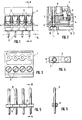
- the terminal strip shown which in practice can of course also have a much higher pole in addition to four poles, has an insulating housing 1 in which screw terminals 2 are arranged insulated from one another in order with the help of a clamping screw 3 to clamp an electrical conductor (not shown) inserted into the insertion opening 4, preferably a conductor protection bracket 5 is provided to prevent the electrical conductor from being squeezed and deformed too much has penetrated opening.
- the sleeve at the lower insertion 10 for the pin 8 has a slightly larger diameter than this, while the diameter in the area of the rounded slotted outlet end should be smaller, so that a smooth transition into the plug position takes place.
- a groove 11 is provided which receives the carrier strip 12 of the pin strip, so that the underside 13 of the insulating housing 1 can lie flat on a printed circuit board 14 into which the pin strip is soldered, so that a completely wobble-free fit is given, without the pin header needing to have a widened support.
Landscapes
- Coupling Device And Connection With Printed Circuit (AREA)
- Multi-Conductor Connections (AREA)
- Connections Arranged To Contact A Plurality Of Conductors (AREA)
Description
- Die Erfindung bezieht sich auf eine Anschlußklemmleiste zum Aufstecken auf Stiftleisten, insbesondere für gedruckte Leiterplatten, mit in einem Isoliergehäuse angeordneten, vorzugsweise mit einem Leiterschutzbügel versehenen Schraubklemmen zum Anschließen von elektrischen Leitern, wobei die Schraubklemmen mit einem Buchsenkontakt für die Stifte verbunden sind.
- Bei den bislang bekannten Anschlußklemmleisten ist zur Bildung eines Buchsenkontakts der Drahtbügel der Oberseite der Schraubklemmen verlängert ausgebildet und mit einer L-förmigen Abwinklung versehen, wobei der freie, im wesentlichen parallel zur Basisfläche der Schraubklemme verlaufende Schenkel eine Ausnehmung aufweist, in der sich die Stifte unter elektrischer Kontaktgabe verklemmen.
- Abgesehen von den Schwierigkeiten mit der Kontaktgabe aufgrund der unvermeidlichen Fertigungstoleranzen und der labilen leichten Verbiegbarkeit der Drahtschutzbügel lassen sich derartige Anschlußklemmleisten nur für relativ große Raster realisieren. Für Rastermaße mit Klemmenabständen von nur 3,5 mm sind die bekannten Anordnungen nicht einsetzbar.
- Darüber hinaus ist auf dem Markt auch bereits eine Anschlußklemmleiste bekanntgeworden, bei welcher der Schraubklemmenkörper verbreitert und mit einer durchgehenden Bohrung versehen ist, wobei die Bohrung im Innern eine erweiterte Kammer zur Aufnahme einer Federkontakthülse bildet. Diese Anordnung ist jedoch außerordentlich kompliziert und teuer in der Herstellung und somit für die Verwendung generell bei Klemmleisten nicht geeignet.
- Eine Anschlußklemme der vorstehend beschriebenen Art ist darüber hinaus auch bereits in der DE-A-3 515 564 beschrieben. Sie zeigt eine Zugbügelklemme, bei der eine Miniaturisierung auf Rastermaß 3,5 mm aus rein maßlichen Gründen nicht mehr realisierbar ist. Darüber hinaus benutzt die Klemme nach der DE-A-3 515 564 als Buchsenkontakt eine verbreiterte Stromschiene mit einer durchgehenden erweiterten Bohrung zur Aufnahme einer Federkontakthülse, was aber wegen der komplexen Anordnung in der Praxis bei Klemmkörpern mit integriertem Buchsenkontakt vermieden werden sollte.
- Der Erfindung liegt daher die Aufgabe zugrunde, eine Anschlußklemmleiste der eingangs genannten Art zu schaffen, die auch bei sehr kleinem Rastermaß noch einfach herstellbar und montierbar ist und gleichzeitig einen guten Kontakt zu den Stiften der Stiftleiste sicherstellt.
- Zur Lösung dieser Aufgabe ist erfindungsgemäß vorgesehen, daß der Buchsenkontakt eine einstückig an dem eine Leiter-Einführöffnung aufweisenden Klemmkörper der Schraubklemme angeformte, an dem der Einstecköffnung für den Stift abgewandten Ende geschlitzte Hülse ist, die sich von der unteren Einstecköffnung, die einen größeren Durchmesser aufweist als die Stifte, auf einen Durchmesser im geschlitzten Ende verjüngt, der kleiner ist als der Stiftdurchmesser.
- Durch die erfindungsgemäße Anordnung ergibt sich die Möglichkeit, die Anschlußklemme in einem sehr viel kleineren Rastermaß zu bauen, als es bei Verwendung des Drahtschutzbügels zusätzlich auch noch als Buchsenkontakt für die Stifte möglich ist. Der erhöhte Bauaufwand durch das Anformen einer geschlitzten Hülse an einem seitlichen Basissteg der Schraubklemme wird durch die einfachere Montage und die erheblich verbesserte Kontaktgabe zu den Stiften weit überkompensiert.
- Die erfindungsgemäße Lösung bietet die Möglichkeit eines sanften Übergangs in die Steckpositon, was bei der bloßen Kontaktgabe des Stifts in einem Loch eines dünnen Blechstreifens selbstverständlich nicht der Fall sein kann. Dieser sanfte Übergang wird dabei besonders durch das Merkmal gestützt, wonach die Hülse so ausgebildet ist, daß sie sich von der unteren Einstecköffnung, die einen etwas größeren Durchmesser aufweist als die Stifte, leicht konisch nach oben auf einen Durchmesser im geschlitzten Austrittsbereich verjüngt, der kleiner ist als der Stiftdurchmesser.
- Schließlich liegt es auch noch im Rahmen der Erfindung, die Anschlußklemmleiste so auszubilden, daß das Isoliergehäuse auf der Unterseite mit einer die Trägerleiste der Stiftleiste aufnehmende Nut versehen ist. Auf diese Art und Weise ergibt sich ein fester wackelfreier Sitz der Anschlußklemmleiste auf einer gedruckten Schaltung, auf die zuvor die Stiftleiste aufgelötet worden ist, ohne daß es besonderer Anformungen oder Verbreiterung der Stiftleiste bedarf.
- Weitere Vorteile, Merkmale und Einzelheiten der Erfindung ergeben sich aus der nachfolgenden Beschreibung eines Ausführungsbeispiels sowie anhand der Zeichnung. Dabei zeigen:
- Fig. 1
- eine Seitenansicht einer erfindungsgemäßen Anschlußklemme in der Aufsetzstellung auf eine in eine gedruckte Leiterplatte eingelöteten Stiftleiste,
- Fig. 2
- einen Schnitt längs der Linie II-II in Fig. 1, wobei die Leiterplatte nicht mit dargestellt ist,
- Fig. 3
- eine Aufsicht auf die Anschlußklemmleiste nach den Figuren 1 und 2,
- Fig. 4
- eine Aufsicht auf eine Schraubklemme mit der seitlich angeformten geschlitzten Hülse,
- Fig. 5
- eine Seitenansicht der Stiftleiste, und
- Fig. 6
- einen Schnitt längs der Linie VI-VI in Fig. 5.
- Die gezeigte Anschlußklemmleiste, die in der Praxis selbstverständlich außer vierpolig auch sehr viel höherpolig ausgebildet sein kann, weist ein Isoliergehäuse 1 auf, in welchem gegeneinander isoliert Schraubklemmen 2 angeordnet sind, um mit Hilfe einer Klemmschraube 3 einen nichtgezeigten, in die Einführöffnung 4 eingesteckten elektrischen Leiter zu verklemmen, wobei bevorzugt ein Leiterschutzbügel 5 zur Verhinderung eines Abquetschens und zu starken Deformierens des elektrischen Leiters vorgesehen ist, der mit seinem auf der Schraubklemme aufliegenden Schenkel eine von der Klemmschraube 3 durchsetzte Öffnung aufweist.
- An einem seitlichen Basissteg 6 der Schraubklemme 2 ist eine langgestreckte, praktisch der gesamten Höhe der Schraubklemme entsprechende Hülse 7 angeformt, die an ihrem der Einstecköffnung für die Stifte 8 einer Stiftleiste 9 abgelegenen oberen Ende geschlitzt ist (vergl. insbesondere Figuren 2 und 4). Wie in Fig. 2 etwas übertrieben angedeutet ist, weist die Hülse am unteren Einführende 10 für den Stift 8 einen etwas größeren Durchmesser auf als dieser, während der Durchmesser im Bereich des gerundeten geschlitzten Austrittsendes kleiner sein soll, so daß ein sanfter Übergang in die Steckposition stattfindet.
- Auf der Unterseite des Isoliergehäuses 1 der Anschlußklemme ist eine Nut 11 vorgesehen, welche die Trägerleiste 12 der Stiftleiste aufnimmt, so daß die Unterseite 13 des Isoliergehäuses 1 flächig auf einer gedruckten Leiterplatte 14, in welche die Stiftleiste eingelötet ist, aufliegen kann, so daß ein völlig wackelfreier Sitz gegeben ist, ohne daß die Stiftleiste eine Auflageverbreiterung aufzuweisen braucht.
Claims (4)
- Anschlußklemmleiste zum Aufstecken auf Stifleisten, insbesondere für gedruckte Leiterplatten, mit in einem Isoliergehäuse angeordneten, vorzugsweise mit einem Leiterschutzbügel versehenen Schraubklemmen zum Anschließen von elektrischen Leitern, wobei die Schraubklemmen mit einem Buchsenkontakt für die Stifte verbunden sind, dadurch gekennzeichnet, daß der Buchsenkontakt eine einstückig an dem eine Leiter-Einführöffnung (4) aufweisenden Klemmkörper der Schraubklemme (2) angeformte, an dem der Einstecköffnung (10) für den Stift (8) abgewandten Ende geschlitzte Hülse (7) ist, die sich von der unteren Einstecköffnung (10), die einen größeren Durchmesser aufweist als die Stifte (8), auf einen Durchmesser im geschlitzten Ende verjüngt, der kleiner ist als der Stiftdurchmesser.
- Anschlußklemmleiste nach Anspruch 1, dadurch gekennzeichnet, daß die Hülse (7) an einem seitlichen Basissteg (6) der Schraubklemme (2) in Abstand von dieser angeformt ist.
- Anschlußklemmleiste nach Anspruch 1 oder 2, dadurch gekennzeichnet, daß die Hülse (7) im Durchmesser leicht konisch nach oben verjüngt ist.
- Anschlußklemmleiste nach einem der Ansprüche 1 bis 3, dadurch gekennzeichnet, daß das Isoliergehäuse (1) auf der Unterseite mit einer eine Trägerleiste (12) der Stiftleiste aufnehmenden Nut (11) versehen ist.
Applications Claiming Priority (2)
| Application Number | Priority Date | Filing Date | Title |
|---|---|---|---|
| DE4132214A DE4132214C2 (de) | 1991-09-27 | 1991-09-27 | Anschlußklemmleiste insbesondere für gedruckte Leiterplatten |
| DE4132214 | 1991-09-27 |
Publications (3)
| Publication Number | Publication Date |
|---|---|
| EP0534063A2 EP0534063A2 (de) | 1993-03-31 |
| EP0534063A3 EP0534063A3 (en) | 1993-11-18 |
| EP0534063B1 true EP0534063B1 (de) | 1996-08-21 |
Family
ID=6441628
Family Applications (1)
| Application Number | Title | Priority Date | Filing Date |
|---|---|---|---|
| EP92110646A Expired - Lifetime EP0534063B1 (de) | 1991-09-27 | 1992-06-24 | Anschlussklemmleiste für gedruckte Leiterplatten |
Country Status (3)
| Country | Link |
|---|---|
| EP (1) | EP0534063B1 (de) |
| DE (2) | DE4132214C2 (de) |
| DK (1) | DK0534063T3 (de) |
Families Citing this family (7)
| Publication number | Priority date | Publication date | Assignee | Title |
|---|---|---|---|---|
| DE19608356B4 (de) * | 1996-02-21 | 2006-04-13 | Wago Verwaltungsgesellschaft Mbh | Elektr. Anschlußklemme |
| DE29606347U1 (de) * | 1996-04-01 | 1997-10-23 | Wieland Electric GmbH, 96052 Bamberg | Elektrischer Steckverbinder, insbesondere für Leiterplatten |
| DE19834681C1 (de) * | 1998-07-31 | 2000-05-11 | Metz Albert Ria Electronic | Anschlußklemme |
| DE10238913A1 (de) * | 2002-08-24 | 2004-03-04 | Valeo Schalter Und Sensoren Gmbh | Verfahren zur Fixierung von elektronischen Steckverbindern |
| DE10254091B4 (de) * | 2002-11-20 | 2015-12-24 | Phoenix Contact Gmbh & Co. Kg | Steckverbinder mit Stiftführung |
| CN107332030B (zh) * | 2016-04-29 | 2019-08-20 | 进联电子科技(上海)有限公司 | 具有输入、输出作用的端子装置 |
| CN110444925B (zh) * | 2019-07-05 | 2021-04-27 | 宁波公牛电器有限公司 | 一种快装接线端子模块及开关 |
Family Cites Families (8)
| Publication number | Priority date | Publication date | Assignee | Title |
|---|---|---|---|---|
| DE1274709B (de) * | 1967-07-19 | 1968-08-08 | Multi Contact Ag | Kontaktleiste |
| US3538240A (en) * | 1968-08-12 | 1970-11-03 | Raychem Corp | Terminal device |
| DE2158506C2 (de) * | 1971-11-25 | 1983-05-19 | Metalluk Karl Anton Bauscher KG, vorm. Johann Cawe, 8600 Bamberg | Anschlußstift für einen Klemmkörper in einer Anschlußleiste für gedruckte Schaltungen |
| DE2409131A1 (de) * | 1974-02-26 | 1975-09-04 | Phoenix Elekt | Elektrische reihenklemme, insbes. schaltanlagen-reihenklemme |
| DE2429714A1 (de) * | 1974-06-20 | 1976-01-08 | Daut & Rietz Kg | Anordnung zum anbringen von runden kontaktstiften od. dgl. in lochungen, insbesondere von leiterplatten |
| CH580342A5 (en) * | 1975-02-18 | 1976-09-30 | Comat Ag | Electrical equipment with screw terminals - has cutout into which terminal block fits when attached to lugs |
| DE3515564A1 (de) * | 1985-04-30 | 1986-10-30 | RIA electronic Albert Metz, 7712 Blumberg | Mehrpolige elektrische anschlussklemme |
| DE9112548U1 (de) * | 1991-10-09 | 1991-12-19 | RIA electronic Albert Metz, 7712 Blumberg | Anschlußklemme |
-
1991
- 1991-09-27 DE DE4132214A patent/DE4132214C2/de not_active Expired - Fee Related
-
1992
- 1992-06-24 DE DE59206942T patent/DE59206942D1/de not_active Expired - Fee Related
- 1992-06-24 DK DK92110646.4T patent/DK0534063T3/da active
- 1992-06-24 EP EP92110646A patent/EP0534063B1/de not_active Expired - Lifetime
Also Published As
| Publication number | Publication date |
|---|---|
| DE4132214A1 (de) | 1993-04-08 |
| EP0534063A3 (en) | 1993-11-18 |
| DE59206942D1 (de) | 1996-09-26 |
| EP0534063A2 (de) | 1993-03-31 |
| DK0534063T3 (da) | 1996-10-28 |
| DE4132214C2 (de) | 1994-05-26 |
Similar Documents
| Publication | Publication Date | Title |
|---|---|---|
| DE69300865T3 (de) | Elektrischer verbinder mit blech als steckkontaktmaterial. | |
| DE60004418T2 (de) | Abzweigverbindergehäuse | |
| DE3514099A1 (de) | Verbindungsklemme fuer elektrische leiter | |
| EP1758206A2 (de) | Vertikale Steckmöglichkeit bei Reihenklemme mit Etagenversatz | |
| EP3375048B1 (de) | Steckkontakt | |
| EP2242327B2 (de) | Elektrische Heizvorrichtung | |
| EP1100150A1 (de) | Zugfederanschluss für grosse Leiterquerschnitte | |
| DE19849267A1 (de) | Steckverbindung einer Leiterkarte an Elektromotor | |
| DE2309138A1 (de) | Elektrischer verbinder | |
| DE2829781A1 (de) | Elektrischer verbinder | |
| DE69303065T2 (de) | Verbinderklemme mit Sattel veränderlicher Dicke und mit eingefasster Mutter | |
| DE7837478U1 (de) | AnschluBteU für elektrische Leitungen | |
| DE19525241A1 (de) | Steckverbinder für gedruckte Schaltungen | |
| EP0822337A2 (de) | Haltevorrichtung für elektrische Lüfter, insbesondere Kleinstlüfter | |
| EP0534063A2 (de) | Anschlussklemmleiste für gedruckte Leiterplatten | |
| DE3030523A1 (de) | Elektrische anschlussklemme | |
| DE102021115257A1 (de) | Verbinder | |
| EP0122314A2 (de) | Mehrpolige Steckverbindung | |
| DE102019111193B3 (de) | Schnittstelle mit Leiterplattenkontakt für Leiterplatte | |
| EP1542319A2 (de) | Elektrische Steckvorrichtung bzw. Steckverbindung | |
| EP1182735B1 (de) | Elektrische Reihenklemme | |
| DE19735786A1 (de) | Schraubenlose Anschlußklemme | |
| DE68918933T2 (de) | Elektrischer Verbinder mit vorgespannten Kontakten und Verfahren zu dessen Herstellung. | |
| DE1954997B2 (de) | Elektrische steckvorrichtung | |
| DE102021132042A1 (de) | Leiteranschlussklemme mit modularem Aufbau und modulares System |
Legal Events
| Date | Code | Title | Description |
|---|---|---|---|
| PUAI | Public reference made under article 153(3) epc to a published international application that has entered the european phase |
Free format text: ORIGINAL CODE: 0009012 |
|
| AK | Designated contracting states |
Kind code of ref document: A2 Designated state(s): BE CH DE DK IT LI NL SE |
|
| PUAL | Search report despatched |
Free format text: ORIGINAL CODE: 0009013 |
|
| AK | Designated contracting states |
Kind code of ref document: A3 Designated state(s): BE CH DE DK IT LI NL SE |
|
| 17P | Request for examination filed |
Effective date: 19931216 |
|
| 17Q | First examination report despatched |
Effective date: 19941117 |
|
| GRAH | Despatch of communication of intention to grant a patent |
Free format text: ORIGINAL CODE: EPIDOS IGRA |
|
| GRAH | Despatch of communication of intention to grant a patent |
Free format text: ORIGINAL CODE: EPIDOS IGRA |
|
| GRAA | (expected) grant |
Free format text: ORIGINAL CODE: 0009210 |
|
| AK | Designated contracting states |
Kind code of ref document: B1 Designated state(s): BE CH DE DK IT LI NL SE |
|
| PG25 | Lapsed in a contracting state [announced via postgrant information from national office to epo] |
Ref country code: NL Free format text: LAPSE BECAUSE OF FAILURE TO SUBMIT A TRANSLATION OF THE DESCRIPTION OR TO PAY THE FEE WITHIN THE PRESCRIBED TIME-LIMIT Effective date: 19960821 |
|
| REG | Reference to a national code |
Ref country code: CH Ref legal event code: NV Representative=s name: ISLER & PEDRAZZINI AG |
|
| REF | Corresponds to: |
Ref document number: 59206942 Country of ref document: DE Date of ref document: 19960926 |
|
| ITF | It: translation for a ep patent filed | ||
| REG | Reference to a national code |
Ref country code: DK Ref legal event code: T3 |
|
| NLV1 | Nl: lapsed or annulled due to failure to fulfill the requirements of art. 29p and 29m of the patents act | ||
| PLBE | No opposition filed within time limit |
Free format text: ORIGINAL CODE: 0009261 |
|
| STAA | Information on the status of an ep patent application or granted ep patent |
Free format text: STATUS: NO OPPOSITION FILED WITHIN TIME LIMIT |
|
| PG25 | Lapsed in a contracting state [announced via postgrant information from national office to epo] |
Ref country code: BE Effective date: 19970630 |
|
| 26N | No opposition filed | ||
| BERE | Be: lapsed |
Owner name: F. WIELAND ELEKTRISCHE INDUSTRIE G.M.B.H. Effective date: 19970630 |
|
| REG | Reference to a national code |
Ref country code: CH Ref legal event code: PFA Free format text: F. WIELAND ELEKTRISCHE INDUSTRIE GMBH TRANSFER- WIELAND ELECTRIC GMBH |
|
| PGFP | Annual fee paid to national office [announced via postgrant information from national office to epo] |
Ref country code: DE Payment date: 20040624 Year of fee payment: 13 |
|
| PGFP | Annual fee paid to national office [announced via postgrant information from national office to epo] |
Ref country code: SE Payment date: 20040628 Year of fee payment: 13 |
|
| PGFP | Annual fee paid to national office [announced via postgrant information from national office to epo] |
Ref country code: DK Payment date: 20040629 Year of fee payment: 13 Ref country code: CH Payment date: 20040629 Year of fee payment: 13 |
|
| PG25 | Lapsed in a contracting state [announced via postgrant information from national office to epo] |
Ref country code: IT Free format text: LAPSE BECAUSE OF NON-PAYMENT OF DUE FEES;WARNING: LAPSES OF ITALIAN PATENTS WITH EFFECTIVE DATE BEFORE 2007 MAY HAVE OCCURRED AT ANY TIME BEFORE 2007. THE CORRECT EFFECTIVE DATE MAY BE DIFFERENT FROM THE ONE RECORDED. Effective date: 20050624 |
|
| PG25 | Lapsed in a contracting state [announced via postgrant information from national office to epo] |
Ref country code: SE Free format text: LAPSE BECAUSE OF NON-PAYMENT OF DUE FEES Effective date: 20050625 |
|
| PG25 | Lapsed in a contracting state [announced via postgrant information from national office to epo] |
Ref country code: LI Free format text: LAPSE BECAUSE OF NON-PAYMENT OF DUE FEES Effective date: 20050630 Ref country code: DK Free format text: LAPSE BECAUSE OF NON-PAYMENT OF DUE FEES Effective date: 20050630 Ref country code: CH Free format text: LAPSE BECAUSE OF NON-PAYMENT OF DUE FEES Effective date: 20050630 |
|
| PG25 | Lapsed in a contracting state [announced via postgrant information from national office to epo] |
Ref country code: DE Free format text: LAPSE BECAUSE OF NON-PAYMENT OF DUE FEES Effective date: 20060103 |
|
| REG | Reference to a national code |
Ref country code: CH Ref legal event code: PL |
|
| EUG | Se: european patent has lapsed | ||
| REG | Reference to a national code |
Ref country code: DK Ref legal event code: EBP |