EP0533137A2 - Leadframe and resin-sealed semiconductor device - Google Patents
Leadframe and resin-sealed semiconductor device Download PDFInfo
- Publication number
- EP0533137A2 EP0533137A2 EP92115849A EP92115849A EP0533137A2 EP 0533137 A2 EP0533137 A2 EP 0533137A2 EP 92115849 A EP92115849 A EP 92115849A EP 92115849 A EP92115849 A EP 92115849A EP 0533137 A2 EP0533137 A2 EP 0533137A2
- Authority
- EP
- European Patent Office
- Prior art keywords
- leadframe
- layer
- layer member
- openings
- etching
- Prior art date
- Legal status (The legal status is an assumption and is not a legal conclusion. Google has not performed a legal analysis and makes no representation as to the accuracy of the status listed.)
- Withdrawn
Links
Images


Classifications
-
- H—ELECTRICITY
- H10—SEMICONDUCTOR DEVICES; ELECTRIC SOLID-STATE DEVICES NOT OTHERWISE PROVIDED FOR
- H10W—GENERIC PACKAGES, INTERCONNECTIONS, CONNECTORS OR OTHER CONSTRUCTIONAL DETAILS OF DEVICES COVERED BY CLASS H10
- H10W70/00—Package substrates; Interposers; Redistribution layers [RDL]
- H10W70/01—Manufacture or treatment
- H10W70/04—Manufacture or treatment of leadframes
- H10W70/042—Etching
-
- H—ELECTRICITY
- H10—SEMICONDUCTOR DEVICES; ELECTRIC SOLID-STATE DEVICES NOT OTHERWISE PROVIDED FOR
- H10W—GENERIC PACKAGES, INTERCONNECTIONS, CONNECTORS OR OTHER CONSTRUCTIONAL DETAILS OF DEVICES COVERED BY CLASS H10
- H10W70/00—Package substrates; Interposers; Redistribution layers [RDL]
- H10W70/40—Leadframes
- H10W70/456—Materials
- H10W70/457—Materials of metallic layers on leadframes
-
- H—ELECTRICITY
- H10—SEMICONDUCTOR DEVICES; ELECTRIC SOLID-STATE DEVICES NOT OTHERWISE PROVIDED FOR
- H10W—GENERIC PACKAGES, INTERCONNECTIONS, CONNECTORS OR OTHER CONSTRUCTIONAL DETAILS OF DEVICES COVERED BY CLASS H10
- H10W70/00—Package substrates; Interposers; Redistribution layers [RDL]
- H10W70/40—Leadframes
- H10W70/411—Chip-supporting parts, e.g. die pads
-
- H—ELECTRICITY
- H10—SEMICONDUCTOR DEVICES; ELECTRIC SOLID-STATE DEVICES NOT OTHERWISE PROVIDED FOR
- H10W—GENERIC PACKAGES, INTERCONNECTIONS, CONNECTORS OR OTHER CONSTRUCTIONAL DETAILS OF DEVICES COVERED BY CLASS H10
- H10W72/00—Interconnections or connectors in packages
- H10W72/50—Bond wires
- H10W72/531—Shapes of wire connectors
- H10W72/536—Shapes of wire connectors the connected ends being ball-shaped
-
- H—ELECTRICITY
- H10—SEMICONDUCTOR DEVICES; ELECTRIC SOLID-STATE DEVICES NOT OTHERWISE PROVIDED FOR
- H10W—GENERIC PACKAGES, INTERCONNECTIONS, CONNECTORS OR OTHER CONSTRUCTIONAL DETAILS OF DEVICES COVERED BY CLASS H10
- H10W72/00—Interconnections or connectors in packages
- H10W72/50—Bond wires
- H10W72/531—Shapes of wire connectors
- H10W72/5363—Shapes of wire connectors the connected ends being wedge-shaped
-
- H—ELECTRICITY
- H10—SEMICONDUCTOR DEVICES; ELECTRIC SOLID-STATE DEVICES NOT OTHERWISE PROVIDED FOR
- H10W—GENERIC PACKAGES, INTERCONNECTIONS, CONNECTORS OR OTHER CONSTRUCTIONAL DETAILS OF DEVICES COVERED BY CLASS H10
- H10W72/00—Interconnections or connectors in packages
- H10W72/50—Bond wires
- H10W72/551—Materials of bond wires
- H10W72/552—Materials of bond wires comprising metals or metalloids, e.g. silver
- H10W72/5522—Materials of bond wires comprising metals or metalloids, e.g. silver comprising gold [Au]
-
- H—ELECTRICITY
- H10—SEMICONDUCTOR DEVICES; ELECTRIC SOLID-STATE DEVICES NOT OTHERWISE PROVIDED FOR
- H10W—GENERIC PACKAGES, INTERCONNECTIONS, CONNECTORS OR OTHER CONSTRUCTIONAL DETAILS OF DEVICES COVERED BY CLASS H10
- H10W74/00—Encapsulations, e.g. protective coatings
-
- H—ELECTRICITY
- H10—SEMICONDUCTOR DEVICES; ELECTRIC SOLID-STATE DEVICES NOT OTHERWISE PROVIDED FOR
- H10W—GENERIC PACKAGES, INTERCONNECTIONS, CONNECTORS OR OTHER CONSTRUCTIONAL DETAILS OF DEVICES COVERED BY CLASS H10
- H10W90/00—Package configurations
- H10W90/701—Package configurations characterised by the relative positions of pads or connectors relative to package parts
- H10W90/751—Package configurations characterised by the relative positions of pads or connectors relative to package parts of bond wires
- H10W90/756—Package configurations characterised by the relative positions of pads or connectors relative to package parts of bond wires between a chip and a stacked lead frame, conducting package substrate or heat sink
Definitions
- the present invention relates to a leadframe, and more particularly to a leadframe for a resin-sealed semiconductor device.
- a conventional type of leadframe 1, 1' is typically constructed in a single layer structure using a single material such as a copper(Cu)-based material or an iron-nickel(Fe-Ni) alloy (generally known as Alloy 42).
- a chip 4 containing a semiconductor integrated circuit is mounted on the upper principal surface of a stage 1 of the leadframe with a conductive adhesive, such as silver(Ag) paste, intervening therebetween for bonding one to the other, and after a pad 7 forming a terminal on the chip 4 is connected to a lead 1' of the leadframe (the tip of the lead 1' is plated with silver(Ag) or the like) using an appropriate lead wire such as gold wire, an appropriate sealing resin 2 is molded to encapsulate the stage 1 of the leadframe, the chip 4, and a portion of the lead 1'; a resin-sealed semiconductor device is thus formed.
- a conductive adhesive such as silver(Ag) paste
- the bonding strength at the interface between stage 1 and resin 2 is weak, imperfections such as voids, cracks, and gaps may be initially contained in the interface, or such voids, cracks, gaps, etc. may be further developed or expanded when stress is applied to the semiconductor device.
- the prior art has employed a method that involves providing throughholes in stage 1 of the leadframe.
- This method results in a significant reduction in the bonding effect, as the conductive adhesive, such as silver paste or solder, enters the throughholes when the chip 4 is mounted on the stage 1.
- the method also involves a reduction in the bonding strength between stage 1 and the chip 4 because of the reduced bonding area between them.
- a leadframe that comprises a body constructed from at least two kinds of layer members formed from different materials and laminated one on top of the other; the materials for the layer members being chosen to have different etching rates.
- a leadframe wherein openings are formed through one layer member and independent hollow spaces communicating with the openings are formed in another layer member.
- a resin-sealed semiconductor device that is constructed by sealing in a resin material the above structured leadframe with an appropriate chip mounted thereon; the sealing resin being made to spread into the hollow spaces through the openings formed on the opposite side of the leadframe from the side thereof on which the chip is mounted.
- the sealing resin is made to spread into the hollow spaces formed in the side of the leadframe stage opposite the chip-mounting side thereof, thereby providing an anchor effect and thus enhancing the adhesion, and hence the bonding strength, at the interface between the resin and the leadframe, and in particular, the stage thereof.
- the leadframe of the present invention allows the use of adhesives having lower viscosity than the adhesives previously used, and thus makes it easier to use such conductive adhesives as silver paste or solder. Thereby enhancing the uniformity and efficiency of the stage-to-chip bonding work and also improving the adhesion between the stage and the resin without reducing the bonding strength between the stage and the chip.
- Fig. 1 is a cross sectional view showing the structure of a leadframe according to one embodiment of the invention.
- Fig. 2 is a cross sectional view showing an example wherein throughholes are formed in a first layer member of the leadframe of the invention.
- Fig. 3 is a cross sectional view showing an example of the structure of the leadframe of the invention.
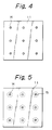
- Fig. 4 is a bottom end plan view of the leadframe of the invention.
- Fig. 5 is a bottom end plan view of the leadframe of the invention.
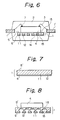
- Fig. 6 is a cross sectional view showing an example of a resin-sealed semiconductor device constructed using the leadframe of the invention.
- Fig. 7 is a cross sectional view showing the structure of a leadframe according to another embodiment of the invention.
- Fig 8 is a cross sectional view showing the structure of a leadframe according to another embodiment of the invention.
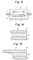
- Fig. 9 is a cross sectional view showing, as an example, the structure of a prior art resin-sealed semiconductor device.
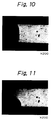
- Fig. 10 is a diagram showing a cross sectional profile of an end portion of a prior art leadframe A treated with complete etching.
- Fig. 11 is a diagram showing a cross sectional profile of the prior art leadframe A treated with half etching.
- Fig. 12 is a diagram showing a cross sectional profile of an end portion of a leadframe B of the present invention, with complete etching.
- Fig. 13 is a diagram showing a cross sectional profile of the leadframe B of the present invention, with half etching.
- Fig. 14 is a diagram showing the conditions of the layers shown in the cross section of Fig. 12.
- Fig. 15 is a diagram showing the conditions of the layers shown in the cross section of Fig. 13.
- Fig. 1 is a cross sectional view showing the structure of a leadframe according to one embodiment of the invention.
- the leadframe in the example shown has a three-layer structure.
- the leadframe comprises a body 1 constructed from at least two kinds of layer members, 11, 12, and 13, formed from different materials and laminated one on top of the other.
- the materials forming the layer members, 11, 12, and 13, are chosen to have different etching rates.
- the uppermost layer member 13 forms the principal surface of the leadframe on which a chip is to be mounted.
- the layer member 11 is hereinafter referred to as the first layer member, the layer member 12 forming the intermediate processing layer as the second layer member, and the layer member 13 as the third layer member.
- each individual layer member is made to have a different etching rate.
- the etching rate of the second layer member is chosen to be the greatest, followed by that of the first layer member, and the etching rate of the third layer member is chosen to be the smallest of the three.
- first and third layer members can be made to have equal etching rates between them but smaller than that of the second layer member, the etching rate of the second layer member being made the greatest of the three.
- the etching rate of each individual layer member can be varied by appropriately changing the material for the layer member.
- the above etching rate scheme can be accomplished by forming the second layer member from a copper-based material and the first and third layer members from an iron-nickel alloy.
- the second layer member 12 having a prescribed etching rate, the first layer member 11 having an etching rate smaller than that of the second layer member, and/or the third layer member 13 having an etching rate smaller than that of the second layer member 12 but equal to or greater than that of the first layer member, are prepared, and these layer members are deposited and joined together by using suitable joining means to provide the structure shown in Fig. 1.
- the first layer member 11 may be preformed with a prescribed number of throughholes 14 opened therein at a prescribed pitch, or alternatively, the layered structure shown in Fig. 1 may be formed first, and then the throughholes may be opened through the first layer member 11.
- part of the material forming the second layer member 12 spreads into the throughholes formed in the first layer member 11.
- the throughholes 14 may not have to be made in the first layer member 11, but instead, may be patterned an the first layer member 11 for etching using a mask or the like having therein suitable openings so that the throughholes 14 are opened during the etching of the first layer member 11.
- the shape of the throughholes 14 is not specifically limited, but any desired shape, circular, polygonal, or oval, may be used.
- the cross sectional area of the throughholes 14 is not specifically limited, but since there is a need to form a large number of independent hollow spaces inside the second layer member 12, as will be described later, it is preferable to determine the cross sectional area by the material for the second layer member 12, the etching rate of the material, the kind of etchant used, etc.
- etching is performed on the thus constructed leadframe 1 of the three-layer structure, to form inside the second layer member 12, independent hollow spaces 15 that communicate with the respective throughholes 14 formed in the first layer member 11.
- An etching of ferric chloride may be chosen as the etching for the present invention.
- the second layer member 12 in the leadframe is etched preferentially to the first layer member 11, so that the hollow spaces 15 are formed independently of each other, as shown in Fig. 3, corresponding to the respective throughholes 14 formed in the first layer member 11.
- the etching condition should be selected to avoid etching the whole second layer member 12 or forming large hollow spaces 15 covering more than one throughhole 14.
- the size of the hollow spaces 15 formed inside the second layer member 12 is not specifically limited; the top 16 of each hollow space 15 may rest within the second layer member 12, or alternatively, the etching may be performed in such a way that the top 16 of each hollow space 15 reaches the third layer member 13, as shown in Fig. 3.
- Figs. 4 and 5 respectively show the bottom end of the first layer member 11 before and after the etching is performed in accordance with the present invention.
- a resin-sealed semiconductor device is constructed using the leadframe of the invention; first, an appropriate chip is attached in place on the principal surface 5 of the stage of the leadframe by using an appropriate adhesive, and then an appropriate sealing resin is molded around the leadframe-chip subassembly, to complete the construction of a resin-sealed semiconductor device.
- Fig. 6 shows an example of the structure of the semiconductor device constructed using the leadframe of the invention.
- the present invention requires the use of more than one layer member to construct the leadframe, at least two kinds of layer members having different etching rates should be used to construct the layered structure, though it is also possible to use four or more kinds of layer members.
- Fig. 7 shows the leadframe 1 of the invention that consists only of the first layer member 11 and the second layer member 12 shown in Fig. 1.
- the etching rate of the second layer member 12 is chosen to be greater than that of the first layer member 11.
- the upper surface 5' of the second layer member 12 serves as the principal surface on which to mount a chip 4. Furthermore, as in the foregoing embodiment, the first layer member 11 is provided with appropriate throughholes 14 opened therein as shown in Fig. 4.
- the same etching process as previously described is performed so that the second layer member 12 in the leadframe is etched preferentially to the first layer member 11; as a result, a large number of individually independent hollow spaces 15 are formed inside the second layer member 12 in correspondence with the respective throughholes 14 formed in the first layer member 11, in the same manner as shown in Fig. 3.
- the etching condition should be selected so that each hollow space 15 will not be etched through the second layer member 12 until the top 16 thereof communicates with the chip-mounting principal surface 5'.
- a leadframe A of 0.15 thickness was made using only Alloy 42, i.e., iron-nickel alloy; as an example of the leadframe of the invention, a leadframe B of a three-layer structure was constructed by attaching Alloy 42 layers 11 and 15, each 0.05 mm thick, on both sides of a central layer 12 of 0.05 mm thick copper(Cu) sheeting.
- Alloy 42 i.e., iron-nickel alloy
- a leadframe B of a three-layer structure was constructed by attaching Alloy 42 layers 11 and 15, each 0.05 mm thick, on both sides of a central layer 12 of 0.05 mm thick copper(Cu) sheeting.
- Etching was performed on the leadframes A and B with an etching solution composed primarily of ferric chloride, the results of which are shown in Figs. 10 through 13.
- Figs. 10 and 12 show cross sectional profiles of end portions of the respective leadframes A and B formed as a result of complete etching; Fig. 10 shows a cross sectional profile of an end portion of the prior art leadframe A with the complete etching, and Fig. 12 shows a cross sectional profile of an end portion of the leadframe B, of the present invention, with the complete etching.
- Figs. 11 and 13 show cross sections of portions of the leadframes A and B after etching was performed under the leadframes A and B, as shown in the figures; the etching process being stopped at an appropriate point halfway through the etching, i.e., in the so-called half etching state; Fig. 11 shows a cross sectional profile of the prior art leadframe A with the half etching, and Fig. 13 shows a cross sectional profile of the leadframe B, of the present invention, with the half etching.
- a projecting edge is formed at the boundary between the first Alloy 42 layer 11 and the second copper layer 12.
- the edge serves as an anchor to prevent the leadframe from separating or breaking away from the molded resin, thus providing an effective prevention against cracking.
- Fig. 14 is a diagram explaining the conditions of the layers shown in the cross section of Fig. 12, and Fig. 15 is a diagram explaining the conditions of the layers shown in cross section of Fig. 13.
- Table 1 shows the results of experiments conducted on the leadframe B of the invention and the leadframe A of the prior art to observe how cracking occurs.
- the leadframe B of the invention dispensed with the half etching, was mounted with a prescribed number of devices and then encapsulated in a molded epoxy resin, after which the completed assembly was dried for 24 hours at a temperature of 125°C and then exposed to a humid environment of 85°C temperature and 85% humidity for 12 hours or 24 hours. Then, after the leadframe B was immersed in molten solder of 260°C for 10 seconds, the resulting chip was visually inspected at randomly selected positions a prescribed number of times to check for the formation of cracks, and count the number of cracks formed.
- the leadframe B of the invention was treated with the half etching to produce a leadframe equivalent to the embodiment of the invention, i.e., the leadframe having the cross section shown in Fig. 13.
- the thus prepared leadframe B was mounted with a prescribed number of devices and then encapsulated in a molded epoxy resin, after which the same processing as in the above experiment was performed and the same observation was conducted.
- the leadframe of the present invention achieves an improvement in the adhesion between the stage of the leadframe and the sealing resin without reducing the bonding strength between the stage of the leadframe and the chip, and thus contributes to enhancing the reliability of semiconductor devices containing semiconductor integrated circuits.
Landscapes
- Lead Frames For Integrated Circuits (AREA)
- Structures Or Materials For Encapsulating Or Coating Semiconductor Devices Or Solid State Devices (AREA)
- Die Bonding (AREA)
Abstract
A leadframe is adapted to enhance the adhesion between a stage 1 and a sealing resin (2) without decreasing the bonding strength between the stage 1 and a chip 4. The leadframe comprises a body 1 constructed from at least two kinds of layer members, 11, 12, and 13, formed from different materials and laminated one on top of the other; the materials for the layer members 11, 12, and 13 being chosen to have different etching rates. Hollow spaces 15 are formed inside the layer member having the greatest etching rate of all the layer members.
Description
- The present invention relates to a leadframe, and more particularly to a leadframe for a resin-sealed semiconductor device.
- As shown in Fig. 9, a conventional type of
leadframe 1, 1' is typically constructed in a single layer structure using a single material such as a copper(Cu)-based material or an iron-nickel(Fe-Ni) alloy (generally known as Alloy 42). In the illustrated construction, achip 4 containing a semiconductor integrated circuit is mounted on the upper principal surface of astage 1 of the leadframe with a conductive adhesive, such as silver(Ag) paste, intervening therebetween for bonding one to the other, and after apad 7 forming a terminal on thechip 4 is connected to a lead 1' of the leadframe (the tip of the lead 1' is plated with silver(Ag) or the like) using an appropriate lead wire such as gold wire, anappropriate sealing resin 2 is molded to encapsulate thestage 1 of the leadframe, thechip 4, and a portion of the lead 1'; a resin-sealed semiconductor device is thus formed. - In a semiconductor device using a leadframe of the above construction, adhesion between the chip and the leadframe and between the leadframe and the sealing resin becomes a problem; while the bonding strength at the interface between the leadframe and the chip has been improved by the improvement of adhesives, the bonding strength at the interface between the
resin 2 and the leadframe, in particular,stage 1 thereof, is not yet sufficient, and improvement in the bonding strength is required. - Specifically, if the bonding strength at the interface between
stage 1 andresin 2 is weak, imperfections such as voids, cracks, and gaps may be initially contained in the interface, or such voids, cracks, gaps, etc. may be further developed or expanded when stress is applied to the semiconductor device. - In particular, if such voids, cracks gaps, etc. are formed in the interface, there is a possibility that the water or moisture initially contained in
resin 2 and furthermore, the external water or moisture subsequently absorbed intoresin 2, will build up in the voids, cracks, gaps, etc. The resulting problem is that when mounting the semiconductor device on a circuit board, the high temperature of soldering (e.g., 215 to 260°C) used in the process will cause the water or moisture to expand in volume, thereby spreading the voids, etc. and thus forming cracks in the semiconductor device. - To overcome the above problem, the prior art has employed a method that involves providing throughholes in
stage 1 of the leadframe. This method, however, results in a significant reduction in the bonding effect, as the conductive adhesive, such as silver paste or solder, enters the throughholes when thechip 4 is mounted on thestage 1. The method also involves a reduction in the bonding strength betweenstage 1 and thechip 4 because of the reduced bonding area between them. - It is an object of the present invention to provide a leadframe that overcomes the above-described shortcomings of the prior art and that can improve the bonding strength between
stage 1 and the sealing resin without reducing the bonding strength betweenstage 1 and thechip 4. - It is another object of the invention to provide a semiconductor device constructed using such a leadframe.
- To achieve the above objects, the present invention employs the technical constitution described below. In a first preferred aspect of the present invention, there is provided a leadframe that comprises a body constructed from at least two kinds of layer members formed from different materials and laminated one on top of the other; the materials for the layer members being chosen to have different etching rates. In a second preferred aspect of the present invention, there is provided a leadframe wherein openings are formed through one layer member and independent hollow spaces communicating with the openings are formed in another layer member. In a third preferred aspect of the present invention, there is provided a resin-sealed semiconductor device that is constructed by sealing in a resin material the above structured leadframe with an appropriate chip mounted thereon; the sealing resin being made to spread into the hollow spaces through the openings formed on the opposite side of the leadframe from the side thereof on which the chip is mounted.
- Since the leadframe of the present invention has the above-described construction, during the molding process the sealing resin is made to spread into the hollow spaces formed in the side of the leadframe stage opposite the chip-mounting side thereof, thereby providing an anchor effect and thus enhancing the adhesion, and hence the bonding strength, at the interface between the resin and the leadframe, and in particular, the stage thereof.
- Furthermore, since no throughholes are formed in the upper chip-mounting surface of the leadframe stage, the leadframe of the present invention allows the use of adhesives having lower viscosity than the adhesives previously used, and thus makes it easier to use such conductive adhesives as silver paste or solder. Thereby enhancing the uniformity and efficiency of the stage-to-chip bonding work and also improving the adhesion between the stage and the resin without reducing the bonding strength between the stage and the chip.
-
- Fig. 1 is a cross sectional view showing the structure of a leadframe according to one embodiment of the invention.
- Fig. 2 is a cross sectional view showing an example wherein throughholes are formed in a first layer member of the leadframe of the invention.
- Fig. 3 is a cross sectional view showing an example of the structure of the leadframe of the invention.
- Fig. 4 is a bottom end plan view of the leadframe of the invention.
- Fig. 5 is a bottom end plan view of the leadframe of the invention.
- Fig. 6 is a cross sectional view showing an example of a resin-sealed semiconductor device constructed using the leadframe of the invention.
- Fig. 7 is a cross sectional view showing the structure of a leadframe according to another embodiment of the invention.
- Fig 8 is a cross sectional view showing the structure of a leadframe according to another embodiment of the invention.
- Fig. 9 is a cross sectional view showing, as an example, the structure of a prior art resin-sealed semiconductor device.
- Fig. 10 is a diagram showing a cross sectional profile of an end portion of a prior art leadframe A treated with complete etching.
- Fig. 11 is a diagram showing a cross sectional profile of the prior art leadframe A treated with half etching.
- Fig. 12 is a diagram showing a cross sectional profile of an end portion of a leadframe B of the present invention, with complete etching.
- Fig. 13 is a diagram showing a cross sectional profile of the leadframe B of the present invention, with half etching.
- Fig. 14 is a diagram showing the conditions of the layers shown in the cross section of Fig. 12.
- Fig. 15 is a diagram showing the conditions of the layers shown in the cross section of Fig. 13.
- The preferred embodiments of the present invention will now be described in detail with reference to the accompanying drawings.
- Fig. 1 is a cross sectional view showing the structure of a leadframe according to one embodiment of the invention. The leadframe in the example shown has a three-layer structure.
- In Fig. 1, the leadframe comprises a
body 1 constructed from at least two kinds of layer members, 11, 12, and 13, formed from different materials and laminated one on top of the other. The materials forming the layer members, 11, 12, and 13, are chosen to have different etching rates. - Here, it is assumed that the
uppermost layer member 13, as shown in Fig. 1, forms the principal surface of the leadframe on which a chip is to be mounted. Thelayer member 11 is hereinafter referred to as the first layer member, thelayer member 12 forming the intermediate processing layer as the second layer member, and thelayer member 13 as the third layer member. - In the above structure, each individual layer member is made to have a different etching rate. In one example, the etching rate of the second layer member is chosen to be the greatest, followed by that of the first layer member, and the etching rate of the third layer member is chosen to be the smallest of the three.
- In another example, the first and third layer members can be made to have equal etching rates between them but smaller than that of the second layer member, the etching rate of the second layer member being made the greatest of the three.
- In the present invention, the etching rate of each individual layer member can be varied by appropriately changing the material for the layer member.
- For example, since the etching rate of a copper(Cu)based material is greater than that of iron-nickel(Fe-Ni) alloy, the above etching rate scheme can be accomplished by forming the second layer member from a copper-based material and the first and third layer members from an iron-nickel alloy.
- Next, in the present invention, the
second layer member 12 having a prescribed etching rate, thefirst layer member 11 having an etching rate smaller than that of the second layer member, and/or thethird layer member 13 having an etching rate smaller than that of thesecond layer member 12 but equal to or greater than that of the first layer member, are prepared, and these layer members are deposited and joined together by using suitable joining means to provide the structure shown in Fig. 1. - In the present invention, the
first layer member 11 may be preformed with a prescribed number ofthroughholes 14 opened therein at a prescribed pitch, or alternatively, the layered structure shown in Fig. 1 may be formed first, and then the throughholes may be opened through thefirst layer member 11. - In the latter case, during the rolling operation for joining the
first layer member 11 to thesecond layer member 12, part of the material forming thesecond layer member 12 spreads into the throughholes formed in thefirst layer member 11. - Also, in the present invention, the
throughholes 14 may not have to be made in thefirst layer member 11, but instead, may be patterned an thefirst layer member 11 for etching using a mask or the like having therein suitable openings so that thethroughholes 14 are opened during the etching of thefirst layer member 11. - The shape of the
throughholes 14 is not specifically limited, but any desired shape, circular, polygonal, or oval, may be used. - Also, the cross sectional area of the
throughholes 14 is not specifically limited, but since there is a need to form a large number of independent hollow spaces inside thesecond layer member 12, as will be described later, it is preferable to determine the cross sectional area by the material for thesecond layer member 12, the etching rate of the material, the kind of etchant used, etc. - Next, in the present invention, etching is performed on the thus constructed
leadframe 1 of the three-layer structure, to form inside thesecond layer member 12, independenthollow spaces 15 that communicate with therespective throughholes 14 formed in thefirst layer member 11. - An etching of ferric chloride, for example, may be chosen as the etching for the present invention.
- In the present invention, during the etching process, the
second layer member 12 in the leadframe is etched preferentially to thefirst layer member 11, so that thehollow spaces 15 are formed independently of each other, as shown in Fig. 3, corresponding to therespective throughholes 14 formed in thefirst layer member 11. - Therefore, in the present invention, the etching condition should be selected to avoid etching the whole
second layer member 12 or forming largehollow spaces 15 covering more than onethroughhole 14. - Also, in the present invention, the size of the
hollow spaces 15 formed inside thesecond layer member 12 is not specifically limited; thetop 16 of eachhollow space 15 may rest within thesecond layer member 12, or alternatively, the etching may be performed in such a way that thetop 16 of eachhollow space 15 reaches thethird layer member 13, as shown in Fig. 3. - Figs. 4 and 5 respectively show the bottom end of the
first layer member 11 before and after the etching is performed in accordance with the present invention. - Furthermore, in the present invention, a resin-sealed semiconductor device is constructed using the leadframe of the invention; first, an appropriate chip is attached in place on the
principal surface 5 of the stage of the leadframe by using an appropriate adhesive, and then an appropriate sealing resin is molded around the leadframe-chip subassembly, to complete the construction of a resin-sealed semiconductor device. - Fig. 6 shows an example of the structure of the semiconductor device constructed using the leadframe of the invention.
- In Fig. 6, the same reference numerals are used to designate the same parts as those in Fig. 9.
- Since the present invention requires the use of more than one layer member to construct the leadframe, at least two kinds of layer members having different etching rates should be used to construct the layered structure, though it is also possible to use four or more kinds of layer members.
- Therefore, as an alternative embodiment of the leadframe of the invention, a leadframe constructed with two layers will be described below with reference to Figs. 7 and 8.
- Fig. 7 shows the
leadframe 1 of the invention that consists only of thefirst layer member 11 and thesecond layer member 12 shown in Fig. 1. - In this embodiment, the etching rate of the
second layer member 12 is chosen to be greater than that of thefirst layer member 11. - The materials for the above layer members can be selected appropriately on the same principle as described in connection with Fig. 1
- In this embodiment, the upper surface 5' of the
second layer member 12 serves as the principal surface on which to mount achip 4. Furthermore, as in the foregoing embodiment, thefirst layer member 11 is provided withappropriate throughholes 14 opened therein as shown in Fig. 4. - After the
leadframe 1 is fabricated by joining the twolayer members second layer member 12 in the leadframe is etched preferentially to thefirst layer member 11; as a result, a large number of individually independenthollow spaces 15 are formed inside thesecond layer member 12 in correspondence with therespective throughholes 14 formed in thefirst layer member 11, in the same manner as shown in Fig. 3. - In this embodiment, however, the etching condition should be selected so that each
hollow space 15 will not be etched through thesecond layer member 12 until the top 16 thereof communicates with the chip-mounting principal surface 5'. - Except for the etching condition, the same conditions as for the foregoing embodiment are employed for this embodiment.
- Next, the advantages of the leadframe of the invention will be described below in comparison with a leadframe constructed in accordance with the prior art method.
- First, as an example of the prior art leadframe, a leadframe A of 0.15 thickness was made using only Alloy 42, i.e., iron-nickel alloy; as an example of the leadframe of the invention, a leadframe B of a three-layer structure was constructed by attaching Alloy 42
layers central layer 12 of 0.05 mm thick copper(Cu) sheeting. - Etching was performed on the leadframes A and B with an etching solution composed primarily of ferric chloride, the results of which are shown in Figs. 10 through 13.
- Figs. 10 and 12 show cross sectional profiles of end portions of the respective leadframes A and B formed as a result of complete etching; Fig. 10 shows a cross sectional profile of an end portion of the prior art leadframe A with the complete etching, and Fig. 12 shows a cross sectional profile of an end portion of the leadframe B, of the present invention, with the complete etching.
- When Figs. 10 and 12 are compared, it can be seen that the center portion was etched at a faster rate in the case of the leadframe constructed according to the present invention.
- Figs. 11 and 13 show cross sections of portions of the leadframes A and B after etching was performed under the leadframes A and B, as shown in the figures; the etching process being stopped at an appropriate point halfway through the etching, i.e., in the so-called half etching state; Fig. 11 shows a cross sectional profile of the prior art leadframe A with the half etching, and Fig. 13 shows a cross sectional profile of the leadframe B, of the present invention, with the half etching.
- When Figs. 11 and 13 are compared, it can be seen that the center portion was etched at a faster rate in the case of the leadframe constructed according to the present invention, causing the
second layer member 12 to be further etched and cut inwardly. - This means that as a result of the half etching of the leadframe of the invention, a projecting edge is formed at the boundary between the first Alloy 42
layer 11 and thesecond copper layer 12. When, for example, an epoxy resin is molded around the leadframe in a subsequent process step, the edge serves as an anchor to prevent the leadframe from separating or breaking away from the molded resin, thus providing an effective prevention against cracking. - Fig. 14 is a diagram explaining the conditions of the layers shown in the cross section of Fig. 12, and Fig. 15 is a diagram explaining the conditions of the layers shown in cross section of Fig. 13.
- Table 1 shows the results of experiments conducted on the leadframe B of the invention and the leadframe A of the prior art to observe how cracking occurs.
- In
Experiment 1, the leadframe B of the invention, dispensed with the half etching, was mounted with a prescribed number of devices and then encapsulated in a molded epoxy resin, after which the completed assembly was dried for 24 hours at a temperature of 125°C and then exposed to a humid environment of 85°C temperature and 85% humidity for 12 hours or 24 hours. Then, after the leadframe B was immersed in molten solder of 260°C for 10 seconds, the resulting chip was visually inspected at randomly selected positions a prescribed number of times to check for the formation of cracks, and count the number of cracks formed. - As a result, in
Experiment 1, when the moisture absorption time was set at 12 hours, cracks were observed at seven positions out of the 10 positions observed, while on the other hand, after 24 hours of moisture absorption, cracks were observed at eight positions out of the 10 positions. - In
Experiment 2, the leadframe B of the invention was treated with the half etching to produce a leadframe equivalent to the embodiment of the invention, i.e., the leadframe having the cross section shown in Fig. 13. The thus prepared leadframe B was mounted with a prescribed number of devices and then encapsulated in a molded epoxy resin, after which the same processing as in the above experiment was performed and the same observation was conducted. - As a result, in
Experiment 2, when the moisture absorption time was set at 12 hours, no cracks were observed at any of the 10 positions observed, while on the other hand, after 24 hours of moisture absorption, cracks were observed only at six positions out of the 10 positions. - In
Experiment 3, the leadframe A of the prior art was treated with the half etching, after which the same processing as above was performed and the same observation was conducted. - As a result, in
Experiment 3, when the moisture absorption time was set at 12 hours, cracks were observed at eight positions out of the 10 positions observed, while on the other hand, after 24 hours of moisture absorption, cracks were observed at all of the 10 positions. - It is apparent from the above experiments that even if the leadframe A of the prior art is treated with the half etching, the separation or gapping between the molded resin and the leadframe can easily occur since no projections that serve as anchors are formed between them.
- On the other hand, in the case of the leadframe of the invention, it can be seen that the projections effectively serve as anchors so that there is little possibility of the bond between the molded resin and the leadframe breaking away or separating and resulting in the formation of cracks.
Table 1 No. Material Half etching Moisture absorption time(H) 85°C·85%RH (Relative Humidity) Package cracks/ Sample size 1 Leadframe B None 12 7/10 24 8/10 2 Leadframe B Half etching 12 0/10 24 6/10 3 Leadframe A Half etching 12 8/10 24 10/10 - With the above described construction, the leadframe of the present invention achieves an improvement in the adhesion between the stage of the leadframe and the sealing resin without reducing the bonding strength between the stage of the leadframe and the chip, and thus contributes to enhancing the reliability of semiconductor devices containing semiconductor integrated circuits.
Claims (7)
- A leadframe comprising a body having openings on a main surface thereof and hollow spaces communicating with each one of said openings, respectively, wherein an inner size of said hollow space being larger than an inner size of said opening.
- A leadframe according to claim 1, wherein said body being constructed from at least a first layer and a second layer each formed from different materials and laminated one on top of the other; the materials for said first and second layers being chosen to have different etching rates; and said openings being formed in said first layer and independent hollow spaces communicating with said openings are formed in said second layer.
- A leadframe according to claim 2, wherein said body is provided with a third layer laminated on a top of said second layer.
- A leadframe wherein a first layer disposed farthest from the chip-mounting surface of said leadframe is chosen to have the smallest etching rate; a second layer disposed inwardly adjacent to said first layer having the smallest etching rate is chosen to have the greatest etching rate, and a third layer forming said chip-mounting surface of said leadframe is chosen to have an etching rate smaller than that of said second layer having the greatest etching rate.
- A leadframe according to claim 2, wherein said first layer is made of an iron-nickel alloy and said second layer is made of a copper-base material.
- A leadframe according to claim 3, wherein said first and third layer are made of an iron-nickel alloy, respectively, and said second layer is made of a copper-base material.
- A resin-sealed semiconductor device constructed by sealing in a resing material a leadframe with an appropriate chip mounted thereon; said leadframe comprising a body having openings on a main surface thereof opposite surface of said leadframe on which said chip is mounted, and hollow spaces communicating with each one of said openings, respectively and an inner size of said hollow space being larger than an inner size of said openings; said sealing resin being made to spread into said hollow spaces through said openings.
Applications Claiming Priority (2)
| Application Number | Priority Date | Filing Date | Title |
|---|---|---|---|
| JP3237952A JPH0575006A (en) | 1991-09-18 | 1991-09-18 | Lead frame and resin sealed semiconductor device |
| JP237952/91 | 1991-09-18 |
Publications (2)
| Publication Number | Publication Date |
|---|---|
| EP0533137A2 true EP0533137A2 (en) | 1993-03-24 |
| EP0533137A3 EP0533137A3 (en) | 1993-11-24 |
Family
ID=17022902
Family Applications (1)
| Application Number | Title | Priority Date | Filing Date |
|---|---|---|---|
| EP19920115849 Withdrawn EP0533137A3 (en) | 1991-09-18 | 1992-09-16 | Leadframe and resin-sealed semiconductor device |
Country Status (4)
| Country | Link |
|---|---|
| US (2) | US5367191A (en) |
| EP (1) | EP0533137A3 (en) |
| JP (1) | JPH0575006A (en) |
| KR (1) | KR970000973B1 (en) |
Cited By (4)
| Publication number | Priority date | Publication date | Assignee | Title |
|---|---|---|---|---|
| EP1253640A3 (en) * | 2001-04-16 | 2004-03-03 | Tyco Electronics Corporation | Improved leadframe-based chip scale package |
| WO2005041272A3 (en) * | 2003-10-16 | 2005-07-21 | Infineon Technologies Ag | Production method and device for improving the bonding between plastic and metal |
| EP1976006A3 (en) * | 2007-03-30 | 2008-11-05 | W.C. Heraeus GmbH | System carrier tape for electronic components |
| US9076776B1 (en) * | 2009-11-19 | 2015-07-07 | Altera Corporation | Integrated circuit package with stand-off legs |
Families Citing this family (22)
| Publication number | Priority date | Publication date | Assignee | Title |
|---|---|---|---|---|
| JP2521230B2 (en) * | 1993-07-09 | 1996-08-07 | 株式会社後藤製作所 | Heat sink for semiconductor device and manufacturing method thereof |
| US5429992A (en) * | 1994-05-25 | 1995-07-04 | Texas Instruments Incorporated | Lead frame structure for IC devices with strengthened encapsulation adhesion |
| US5773895A (en) * | 1996-04-03 | 1998-06-30 | Intel Corporation | Anchor provisions to prevent mold delamination in an overmolded plastic array package |
| US5939775A (en) * | 1996-11-05 | 1999-08-17 | Gcb Technologies, Llc | Leadframe structure and process for packaging intergrated circuits |
| JP2877122B2 (en) * | 1997-01-20 | 1999-03-31 | ソニー株式会社 | Semiconductor device and lead frame |
| JP3481117B2 (en) | 1998-02-25 | 2003-12-22 | 富士通株式会社 | Semiconductor device and manufacturing method thereof |
| US5880520A (en) * | 1998-03-31 | 1999-03-09 | Micron Technology, Inc. | Low mutual inductance lead frame device |
| US6143981A (en) | 1998-06-24 | 2000-11-07 | Amkor Technology, Inc. | Plastic integrated circuit package and method and leadframe for making the package |
| TW446627B (en) * | 1998-09-30 | 2001-07-21 | Toyo Kohan Co Ltd | A clad sheet for lead frame, a lead frame using thereof and a manufacturing method thereof |
| US6184064B1 (en) * | 2000-01-12 | 2001-02-06 | Micron Technology, Inc. | Semiconductor die back side surface and method of fabrication |
| US6294409B1 (en) | 2000-01-27 | 2001-09-25 | Siliconware Precisionware Industries Co., Ltd. | Method of forming a constricted-mouth dimple structure on a leadframe die pad |
| JP2001320007A (en) | 2000-05-09 | 2001-11-16 | Dainippon Printing Co Ltd | Frame for resin-encapsulated semiconductor device |
| JP4840893B2 (en) * | 2000-05-12 | 2011-12-21 | 大日本印刷株式会社 | Resin-encapsulated semiconductor device frame |
| JP2004507111A (en) * | 2000-08-18 | 2004-03-04 | コーニンクレッカ フィリップス エレクトロニクス エヌ ヴィ | Method for manufacturing semiconductor device and support substrate and semiconductor device obtained by the method |
| JP2002368176A (en) * | 2001-06-11 | 2002-12-20 | Rohm Co Ltd | Lead frames for semiconductor electronic components |
| US20030178707A1 (en) * | 2002-03-21 | 2003-09-25 | Abbott Donald C. | Preplated stamped small outline no-lead leadframes having etched profiles |
| US20040124505A1 (en) * | 2002-12-27 | 2004-07-01 | Mahle Richard L. | Semiconductor device package with leadframe-to-plastic lock |
| US6879050B2 (en) * | 2003-02-11 | 2005-04-12 | Micron Technology, Inc. | Packaged microelectronic devices and methods for packaging microelectronic devices |
| DE102005003390B4 (en) * | 2005-01-24 | 2007-09-13 | Qimonda Ag | Substrate for an FBGA semiconductor device |
| CN102224586B (en) * | 2008-09-25 | 2013-12-11 | Lg伊诺特有限公司 | Structure and manufacturing method of multi-row lead frame and semiconductor package |
| JP6439489B2 (en) * | 2015-02-19 | 2018-12-19 | 三菱マテリアル株式会社 | Power module substrate manufacturing method and power module manufacturing method |
| JP7653882B2 (en) | 2021-09-22 | 2025-03-31 | 株式会社東芝 | Semiconductor Device |
Family Cites Families (25)
| Publication number | Priority date | Publication date | Assignee | Title |
|---|---|---|---|---|
| JPS5334484A (en) * | 1976-09-10 | 1978-03-31 | Toshiba Corp | Forming method for multi layer wiring |
| JPS54100676A (en) * | 1978-01-26 | 1979-08-08 | Toshiba Corp | Manufacture of semiconductor device |
| JPH0612796B2 (en) * | 1984-06-04 | 1994-02-16 | 株式会社日立製作所 | Semiconductor device |
| JPS63132466A (en) * | 1986-11-22 | 1988-06-04 | Nippon Steel Corp | Material for lead frame |
| US4942452A (en) * | 1987-02-25 | 1990-07-17 | Hitachi, Ltd. | Lead frame and semiconductor device |
| JPH0680760B2 (en) * | 1987-03-13 | 1994-10-12 | 株式会社日立製作所 | Lead frame and semiconductor device |
| JPS63213362A (en) * | 1987-02-27 | 1988-09-06 | Mitsubishi Electric Corp | Resin sealed semiconductor device |
| JPS63239967A (en) * | 1987-03-27 | 1988-10-05 | Toshiba Corp | Resin sealed semiconductor device and manufacture thereof |
| JPH01129448A (en) * | 1987-11-16 | 1989-05-22 | Hitachi Ltd | Lead frame |
| JP2531963B2 (en) * | 1987-12-03 | 1996-09-04 | 新光電気工業株式会社 | Semiconductor device |
| JP2536564B2 (en) * | 1987-12-10 | 1996-09-18 | 三菱電機株式会社 | Resin-sealed semiconductor device |
| JP2593912B2 (en) * | 1988-04-29 | 1997-03-26 | 新光電気工業株式会社 | Lead frame |
| JPH02129948A (en) * | 1988-11-09 | 1990-05-18 | Dainippon Printing Co Ltd | Pre-molded type semiconductor device |
| JPH02246359A (en) * | 1989-03-20 | 1990-10-02 | Fujitsu Ltd | Semiconductor device |
| JPH0318048A (en) * | 1989-06-14 | 1991-01-25 | Matsushita Electron Corp | Semiconductor device |
| JP2797542B2 (en) * | 1989-11-06 | 1998-09-17 | ソニー株式会社 | Lead frame manufacturing method |
| JPH03159163A (en) * | 1989-11-16 | 1991-07-09 | Shinko Electric Ind Co Ltd | Lead frame |
| JPH07109869B2 (en) * | 1989-12-01 | 1995-11-22 | 日立金属株式会社 | Lead frame material |
| JPH0787235B2 (en) * | 1989-12-19 | 1995-09-20 | 凸版印刷株式会社 | Material for lead frame for semiconductor device and method for manufacturing lead frame for semiconductor device |
| JPH03188658A (en) * | 1989-12-19 | 1991-08-16 | Toppan Printing Co Ltd | Lead frame material for semiconductor device and manufacture of lead flame for semiconductor device |
| JPH03188656A (en) * | 1989-12-19 | 1991-08-16 | Toppan Printing Co Ltd | Lead frame material for semiconductor device and manufacture of lead frame for semiconductor device |
| JPH03188659A (en) * | 1989-12-19 | 1991-08-16 | Toppan Printing Co Ltd | Lead frame for semiconductor integrated circuit |
| JPH03188660A (en) * | 1989-12-19 | 1991-08-16 | Toppan Printing Co Ltd | Lead frame material for semiconductor device and manufacture of lead frame for semiconductor device |
| JPH04283953A (en) * | 1991-03-12 | 1992-10-08 | Dainippon Printing Co Ltd | Lead frame material for semiconductor, and manufacture of lead frame |
| JPH05129512A (en) * | 1991-10-31 | 1993-05-25 | Nec Corp | Lead frame |
-
1991
- 1991-09-18 JP JP3237952A patent/JPH0575006A/en active Pending
-
1992
- 1992-09-16 US US07/945,713 patent/US5367191A/en not_active Expired - Lifetime
- 1992-09-16 EP EP19920115849 patent/EP0533137A3/en not_active Withdrawn
- 1992-09-18 KR KR1019920017066A patent/KR970000973B1/en not_active Expired - Fee Related
-
1994
- 1994-09-30 US US08/314,269 patent/US5753535A/en not_active Expired - Fee Related
Cited By (6)
| Publication number | Priority date | Publication date | Assignee | Title |
|---|---|---|---|---|
| EP1253640A3 (en) * | 2001-04-16 | 2004-03-03 | Tyco Electronics Corporation | Improved leadframe-based chip scale package |
| US7034382B2 (en) | 2001-04-16 | 2006-04-25 | M/A-Com, Inc. | Leadframe-based chip scale package |
| WO2005041272A3 (en) * | 2003-10-16 | 2005-07-21 | Infineon Technologies Ag | Production method and device for improving the bonding between plastic and metal |
| EP1976006A3 (en) * | 2007-03-30 | 2008-11-05 | W.C. Heraeus GmbH | System carrier tape for electronic components |
| DE102007015817B4 (en) * | 2007-03-30 | 2011-11-10 | W.C. Heraeus Gmbh | System carrier tape for electronic components |
| US9076776B1 (en) * | 2009-11-19 | 2015-07-07 | Altera Corporation | Integrated circuit package with stand-off legs |
Also Published As
| Publication number | Publication date |
|---|---|
| KR930006884A (en) | 1993-04-22 |
| US5753535A (en) | 1998-05-19 |
| JPH0575006A (en) | 1993-03-26 |
| US5367191A (en) | 1994-11-22 |
| KR970000973B1 (en) | 1997-01-21 |
| EP0533137A3 (en) | 1993-11-24 |
Similar Documents
| Publication | Publication Date | Title |
|---|---|---|
| US5367191A (en) | Leadframe and resin-sealed semiconductor device | |
| US7943431B2 (en) | Leadless semiconductor package and method of manufacture | |
| US7709935B2 (en) | Reversible leadless package and methods of making and using same | |
| KR100687548B1 (en) | Semiconductor wafer manufacturing method, semiconductor device manufacturing method and chip size semiconductor wafer package manufacturing method | |
| US7262491B2 (en) | Die pad for semiconductor packages and methods of making and using same | |
| KR100381837B1 (en) | plastic integrated circuit device package and micro-leadframe and method for making the package | |
| US6451627B1 (en) | Semiconductor device and process for manufacturing and packaging a semiconductor device | |
| US7439097B2 (en) | Taped lead frames and methods of making and using the same in semiconductor packaging | |
| US8963301B1 (en) | Integrated circuit package and method of making the same | |
| US6828688B2 (en) | Resin-sealed semiconductor device, circuit member used for the device, and method of manufacturing the circuit member | |
| KR102227588B1 (en) | Semiconductor device and method of manufacturing the same | |
| US7227245B1 (en) | Die attach pad for use in semiconductor manufacturing and method of making same | |
| JPH09330997A (en) | Semiconductor package substrate and ball grid array semiconductor package | |
| US7214326B1 (en) | Increased capacity leadframe and semiconductor package using the same | |
| US7186588B1 (en) | Method of fabricating a micro-array integrated circuit package | |
| DE102005006730A1 (en) | Lead frame for semiconductor chip package comprises leads on four sides of frame and tie bars extending from side edges and having recessed bottom surfaces | |
| US20030045084A1 (en) | Method of production of semiconductor module | |
| JP2000082759A (en) | Method of manufacturing BGA type semiconductor device, TAB tape for BGA type semiconductor device, and BGA type semiconductor device | |
| US11817375B2 (en) | High I/O density flip-chip QFN | |
| KR101375175B1 (en) | Lead frame, method of manufacturing the lead frame, semiconductor package using the same and method of manufacturing the semiconductor package | |
| KR100349362B1 (en) | Wafer level package and method of fabricating the same | |
| JP2008066491A (en) | Semiconductor device substrate and semiconductor device using the same | |
| KR100370479B1 (en) | Lead frame of semiconductor package | |
| KR19980044619U (en) | Semiconductor package | |
| JPH0311641A (en) | Semiconductor device |
Legal Events
| Date | Code | Title | Description |
|---|---|---|---|
| PUAI | Public reference made under article 153(3) epc to a published international application that has entered the european phase |
Free format text: ORIGINAL CODE: 0009012 |
|
| AK | Designated contracting states |
Kind code of ref document: A2 Designated state(s): DE FR GB |
|
| PUAL | Search report despatched |
Free format text: ORIGINAL CODE: 0009013 |
|
| AK | Designated contracting states |
Kind code of ref document: A3 Designated state(s): DE FR GB |
|
| 17P | Request for examination filed |
Effective date: 19940517 |
|
| 17Q | First examination report despatched |
Effective date: 19960418 |
|
| 18D | Application deemed to be withdrawn |
Effective date: 19960829 |