EP0527636B1 - Circuit compteur utilisant un compteur du type Johnson et son application - Google Patents
Circuit compteur utilisant un compteur du type Johnson et son application Download PDFInfo
- Publication number
- EP0527636B1 EP0527636B1 EP92307330A EP92307330A EP0527636B1 EP 0527636 B1 EP0527636 B1 EP 0527636B1 EP 92307330 A EP92307330 A EP 92307330A EP 92307330 A EP92307330 A EP 92307330A EP 0527636 B1 EP0527636 B1 EP 0527636B1
- Authority
- EP
- European Patent Office
- Prior art keywords
- flip
- counter
- circuit
- data
- stage
- Prior art date
- Legal status (The legal status is an assumption and is not a legal conclusion. Google has not performed a legal analysis and makes no representation as to the accuracy of the status listed.)
- Expired - Lifetime
Links
Images


Classifications
-
- H—ELECTRICITY
- H03—ELECTRONIC CIRCUITRY
- H03K—PULSE TECHNIQUE
- H03K21/00—Details of pulse counters or frequency dividers
-
- H—ELECTRICITY
- H03—ELECTRONIC CIRCUITRY
- H03M—CODING; DECODING; CODE CONVERSION IN GENERAL
- H03M9/00—Parallel/series conversion or vice versa
-
- H—ELECTRICITY
- H03—ELECTRONIC CIRCUITRY
- H03K—PULSE TECHNIQUE
- H03K23/00—Pulse counters comprising counting chains; Frequency dividers comprising counting chains
- H03K23/40—Gating or clocking signals applied to all stages, i.e. synchronous counters
- H03K23/50—Gating or clocking signals applied to all stages, i.e. synchronous counters using bi-stable regenerative trigger circuits
- H03K23/54—Ring counters, i.e. feedback shift register counters
- H03K23/542—Ring counters, i.e. feedback shift register counters with crossed-couplings, i.e. Johnson counters
Definitions
- the present invention relates to a counter circuit, more particularly, to a counter circuit using a Johnson-type counter and its applications.
- the counter circuit and its applied circuits according to the present invention can be utilized in various digital applied circuits which frequently need operations for converting a chain of serial data into parallel data of a plurality of bits, or converting parallel data of a plurality of bits into a chain of serial data.
- a 1/N frequency-dividing circuit including a plurality of flip-flops connected in a cascade connection.
- the first stage flip-flop receives a clock signal and the last stage flip-flop outputs a 1/N divided signal. Accordingly, the 1/N divided signal cannot be obtained until the clock signal is applied and then passed through the flip-flops of the plurality of stages. Namely, it takes considerable time corresponding to an operation delay time of the flip-flops to obtain the 1/N divided signal. This is disadvantageous from a viewpoint of the operation speed.
- each signal input to the OR logic portion needs an input amplitude of a predetermined level. Where the input amplitude is increased, however, a problem occurs in that the operation delay time of each flip-flop is prolonged. This leads to a lowering in a maximum operation frequency of the Johnson-type counter and thus is not preferable.
- a counter circuit including: Johnsontype counters of m stages, each counter including a plurality of flip-flops connected in a cascade connection, each flip-flop receiving a clock signal at a respective clock input end, wherein signals at respective output ends of all flip-flops in a (K-1)th stage counter are simultaneously input to each clock input end of all flip-flops in each counter of a kth stage and more, via respective OR gates.
- a counter circuit including: Johnson-type counters of m stages, each counter including a plurality of flip-flops connected in a cascade connection; and (m-l) logic gates connected between each stage of the Johnson-type counters, wherein a clock signal is simultaneously input to respective clock input ends of flip-flops in a first stage counter; a logic sum of the clock signal and signals at respective output ends of flip-flops in the first stage counter is generated by a first logic gate and output as a first signal; the first signal is simultaneously input to respective clock input ends of flip-flops in a second stage counter; a logic sum of the first signal and signals at respective output ends of flip-flops in the second stage counter is generated by a second logic gate and output as a second signal; and, hereinafter in the like manner, a (m-l)-th signal is simultaneously input to respective clock input ends of flip-flops in a m-th stage counter.
- the present invention provides a counter circuit which can obtain a signal having an arbitrary ratio of frequency division with high speed, while relatively simplifying the circuit constitution.
- the present invention also provides a counter circuit using a Johnson-type counter which can heighten a maximum operation frequency thereof and thus realize a high speed operation thereof.
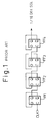
- Figure 1 illustrates a constitution of a prior art 1/16 frequency-dividing circuit
- Fig. 2 shows a timing chart representing the operation thereof.
- the circuit of Fig. 1 includes four flip-flops FF1 to FF4.
- the first stage flip-flop FF1 receives a clock signal CLK at a clock input end C and, hereinafter in the like manner, the following stage flip-flop receives a signal from an output end Q of the preceding stage flip-flop at the clock input end C.
- the last stage flip-flop FF4 outputs a 1/16 divided signal from the output end Q. Accordingly, as shown in the timing chart of Fig. 2, time taken until the 1/16 divided signal is obtained from a point of time of the application of the clock signal CLK is t 4F corresponding to an operation delay time of the flip-flops of four stages.
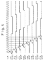
- Figure 3 illustrates a constitution of another prior art 1/16 frequency-dividing circuit
- Fig. 4 shows a timing chart representing the operation thereof.
- the circuit of Fig. 3 has a form of a Johnson-type counter including eight flip-flops FF1 to FF8 connected in a cascade connection. Each flip-flop simultaneously receives a clock signal CLK at a respective clock input end C and the last stage flip-flop FF8 outputs a 1/16 divided signal from the output end Q. According to the constitution, as shown in the timing chart of Fig. 4, time taken until the 1/16 divided signal is obtained from a point of time of the application of the clock signal CLK is no more than t F corresponding to an operation delay time of the flip-flop of one stage. On the other hand, the number of flip-flops used in the constitution is no less than eight.
- Figure 5 illustrates a constitution of a prior art divided signal generating circuit
- Fig. 6 shows a timing chart representing the operation thereof.
- the illustrated circuit 10b includes a logical OR gate LG in addition to the 1/16 frequency-dividing circuit of Fig. 3.
- the OR gate LG generates a logic sum of the clock signal CLK and signals at respective output ends Q of all of the flip-flops FF1 to FF8 and outputs a result thereof as a data load pulse DLP.
- time taken until the data load pulse DLP is obtained from a point of time of the application of the clock signal CLK is no more than t G corresponding to an operation delay time of the gate of one stage.
- the number of flip-flops used in the constitution is no less than eight.
- Figure 7 illustrates a constitution of a prior art 16-bit data demultiplexer circuit
- Fig. 8 shows a timing chart representing the operation thereof.
- the illustrated circuit includes the divided signal generating circuit 10b of Fig. 5, a delay circuit DLY for generating a delayed clock signal DCLK in response to the clock signal CLK, a serial/parallel converting circuit having sixteen flip-flops FF 101 to FF 1 16 connected in a cascade connection, and a latch circuit having sixteen flip-flops FF 201 to FF 2 16 , each flip-flop responsive to the data load pulse DLP output from the divided signal generating circuit 10b, latching respective outputs of the serial/parallel converting circuit and outputting the latched data as parallel data OUT16 to OUT1.
- the delay circuit DLY has the function of delaying the clock signal CLK by a predetermined delay time corresponding to the number of stage of gates and outputting the delayed clock signal DCLK.
- the divided signal generating circuit 10b has the function of outputting the data load pulse DLP at an appropriate timing after data is set in the flip-flops FF 201 to FF 2 16 of the latch circuit.
- the serial/parallel converting circuit sequentially inputs a chain of serial data D in response to the delayed clock signal DCLK, and outputs the parallel data OUT16 to OUT1 in response to the data load pulse DLP and holds the parallel data until a next 16-bit data is input thereto.
- An example of the art is disclosed, for example, in Japanese unexamined patent publication No.3-22712.
- Figure 9 illustrates a constitution of a prior art 16-bit data multiplexer circuit
- Fig. 10 shows a timing chart representing the operation thereof.
- the illustrated circuit includes the divided signal generating circuit 10b of Fig. 5, a delay circuit DLY for generating a delayed clock signal DCLK in response to the clock signal CLK, and a parallel/serial converting circuit having sixteen selectors SEL 01 to SEL 1 6 and sixteen flip-flops FF 3 01 to FF 316 connected sequentially and alternately to one another.
- the delay circuit DLY has the function of delaying the clock signal CLK by a predetermined delay time corresponding to the number of stage of gates and outputting the delayed clock signal DCLK.
- the divided signal generating circuit 10b has the function of outputting the data load pulse DLP when a new 16-bit data is taken into the parallel/serial converting circuit by the selectors SEL 01 to SEL 16 .
- the parallel/serial converting circuit inputs a 16-bit data by means of the selectors SEL 01 to SEL 1 6 in response to the data load pulse DLP and then, in response to the delayed clock signal DCLK, outputs the 16-bit parallel data as a chain of serial data OUT, bit by bit.
- the 1/16 divided signal cannot be obtained until the clock signal CLK is applied to the first stage flip-flop FF1 and then passed through the flip-flops of four stages (FF1 to FF4). Namely, it takes the time t 4F corresponding to the operation delay time of the flip-flops of four stages to obtain the 1/16 divided signal. This is disadvantageous from a viewpoint of the operation speed.
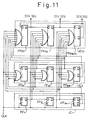
- Figure 11 illustrates a fundamental constitution of the counter circuit according to a first aspect of the present invention.
- the illustrated circuit includes Johnson-type counters JC 1 ⁇ JCm of m stages, each counter including a plurality of flip-flops FF 11 ⁇ FF 1N 1 ,FF 21 ⁇ FF 2N 2 ,... ...,FF m1 ⁇ FF mNm connected in a cascade connection, each flip-flop receiving a clock signal CLK at a respective clock input end C, wherein signals at respective output ends Q of flip-flops in a (k-1)-th stage counter are simultaneously input to respective clock input ends C of flip-flops in each counter of a k-th stage and more.
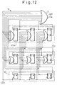
- Figure 12 illustrates a fundamental constitution of the divided signal generating circuit according to a second aspect of the present invention.
- the illustrated circuit includes the counter circuit shown in Fig. 11, and a logic gate LG which generates a logic sum of the clock signal and signals at respective output ends of all of the flip-flops in the counter circuit and outputs a result thereof as a m-th signal.
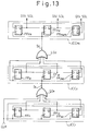
- Figure 13 illustrates a fundamental constitution of the counter circuit according to a third aspect of the present invention.
- the illustrated circuit includes Johnson-type counters JCC 1 ⁇ JCCm of m stages, each counter including a plurality of flip-flops FF 11 ⁇ FF 1N 1 , FF 21 ⁇ FF 2N 2 ,... ... FF m1 ⁇ FF mNm connected in a cascade connection, and (m-1) logic gates LG 1 ⁇ LG m-1 connected between each stage of the Johnson-type counters, wherein a clock signal CLK is simultaneously input to respective clock input ends C of flip-flops in a first stage counter JCC 1 ; a logic sum of the clock signal and signals at respective output ends Q of flip-flops in the first stage counter is generated by a first logic gate LG 1 and output as a first signal S 1 ; the first signal is simultaneously input to respective clock input ends C of flip-flops in a second stage counter JCC 2 ; a logic sum of the first signal and signals at respective output ends Q of flip-flops in the second stage counter is generated by a second logic gate LG 2 and output as
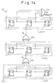
- Figure 14 illustrates a fundamental constitution of the divided signal generating circuit according to a fourth aspect of the present invention.
- the illustrated circuit includes the counter circuit shown in Fig. 13, and a logic gate LGm which generates a logic sum of the (m-1)-th signal and signals at respective output ends of flip-flops in the m-th stage counter and outputs a result thereof as a m-th signal Sm (DLP).
- LGm which generates a logic sum of the (m-1)-th signal and signals at respective output ends of flip-flops in the m-th stage counter and outputs a result thereof as a m-th signal Sm (DLP).
- Figure 15 illustrates a fundamental constitution of the data converting circuit according to a fifth aspect of the present invention.
- the illustrated circuit includes the divided signal generating circuit 10 (20) shown in Fig. 12 or Fig. 14, a unit 11 for inputting a serial data SD in response to the clock signal CLK and converting the serial data into a parallel data PD of a plurality of bits, and a unit 12 for latching and outputting the parallel data in response to the m-th signal DLP output from the divided signal generating circuit.
- Figure 16 illustrates a fundamental constitution of the data converting circuit according to a sixth aspect of the present invention.
- the illustrated circuit includes the divided signal generating circuit 10 (20) shown in Fig. 12 or Fig. 14, and a unit 13 for inputting a parallel data PD of a plurality of bits in response to the m-th signal DLP output from the divided signal generating circuit and converting the parallel data into a serial data SD in response to the clock signal CLK, to thereby output the converted serial data.
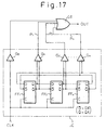
- Figure 17 illustrates a fundamental constitution of a counter circuit.
- the illustrated circuit includes a Johnson-type counter JC including a plurality of flip-flops FF 1 ⁇ FFn connected in a cascade connection, each flip-flop simultaneously receiving a clock signal CLK at a respective clock input end C, and a gate unit GT for generating a logic sum of the clock signal and signals at respective output ends Q, QX of the flip-flops in the counter.
- a Johnson-type counter JC including a plurality of flip-flops FF 1 ⁇ FFn connected in a cascade connection, each flip-flop simultaneously receiving a clock signal CLK at a respective clock input end C, and a gate unit GT for generating a logic sum of the clock signal and signals at respective output ends Q, QX of the flip-flops in the counter.
- the Johnson-type counter includes a buffer unit G 0 , G 1 ⁇ Gn for regulating respective timings at which the clock signal and the signals at the respective output ends of each flip-flop are input to the gate unit, non-inverting and inverting outputs of a last stage flip-flop FFn being input to data inverting and data non-inverting input ends of a first stage flip-flop FF 1 , respectively, and operation amplitude levels of respective differential signal outputs of the flip-flops being set to be smaller than those of other circuits.
- the ratio of frequency division is expressed as follows: 1 / ⁇ 2 ⁇ (N 1 ) ⁇ ⁇ 1 / ⁇ 2 ⁇ (N 2 ) ⁇ ⁇ 1 / ⁇ 2 ⁇ (N 3 ) ⁇ ⁇ ⁇ ⁇ ⁇ ⁇ ⁇ 1 / ⁇ 2 ⁇ (Nm) ⁇
- Nm denotes the number of flip-flops in the m-th stage counter JCm (JCCm), where m indicates an integer more than two (m ⁇ 2).
- JCCm the number of flip-flops in the m-th stage counter JCm
- buffer gates G 0 and G 1 ⁇ Gn are provided for regulating respective timings at which the clock signal CLK and the signals at the respective output ends of each flip-flop are input to the gate means (OR gate GT).
- Each buffer gate G 1 , G 2 ,... ... , Gn receives a differential signal of small amplitude from the corresponding flip-flop, and amplifies the differential signal up to an amplitude level which is necessary and sufficient for the logic operation in the OR gate GT.
- the buffer gate G 0 functions as a gate for phase regulation.
- reference T denotes a period of the clock signal CLK; reference t F an operation delay time of the flip-flop of one stage; reference t G1 an operation delay time of each buffer gate G 0 ⁇ Gn; and reference t G2 an operation delay time of the OR gate GT.
- the non-inverting output Q of the last stage flip-flop FFn remains “L” level until the application of the (n-1)-th clock signal CLK(n-1) and, when the n-th clock signal CLK(n) is applied, the output Q of the flip-flop FFn is made "H” level after a lapse of the delay time of (t F + t G1 ). Also, when the 2n-th clock signal CLK(2n) is applied, the output Q of the flip-flop FFn is made "L” level after a lapse of the delay time of (t F + t G1 ). As a result, the outputs Q of each flip-flop FF 1 to FFn are all brought to "L" level (initial state).
- the outputs Q of all of the flip-flops are brought to "L" level every time the clock signal CLK is input 2n times.
- the edge of the clock signal CLK passing through the buffer gate G 0 becomes effective, and thus the OR gate GT outputs a pulse as shown by reference t x in Fig. 18.
- the pulse width t x is determined by a condition 1 after a lapse of the operation delay time t G1 of the buffer gate G 0 from the fall edge of the clock signal CLK passing through the gate G 0 , or a condition 2 after a lapse of the operation delay times t F and t G1 of the flip-flop FFn and the buffer gate Gn from the rise edge of the clock signal CLK.
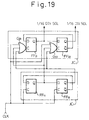
- Figure 19 illustrates a constitution of the 1/16 frequency-dividing circuit according to an embodiment corresponding to the first aspect of the present invention
- Fig. 20 shows a timing chart representing the operation thereof.
- the circuit of Fig. 19 includes Johnson-type counters JC 1 and JC 2 of two stages.
- Signals at respective output ends Q of the flip-flops FF 11 , FF 1 2 in the first stage counter JC 1 are input via OR gates G 2 1 and G 2 2 in the second stage counter JC 2 to respective clock input ends C of the flip-flops FF 21 , FF 2 2 in the counter JC 2 .
- a clock signal CLK is input to the respective clock input ends C of the flip-flops FF 11 , FF 1 2 in the first stage counter JC 1 , and input via the OR gates G 21 , G 2 2 in the second stage counter JC 2 to the respective clock input ends C of the flip-flops FF 21 , FF 22 .
- the flip-flops FF 21 , FF 22 in the second stage counter JC 2 output a 1/16 divided signal from the respective output ends Q.
- reference t F denotes an operation delay time of the flip-flop of one stage.
- time taken until the 1/16 divided signal is obtained from a point of time of the application of the clock signal CLK is no more than t F corresponding to the operation delay time of the flip-flop of one stage (FF 1 1 or FF 12 ).
- the 1/16 divided signal cannot be obtained until the clock signal CLK is applied to the first stage flip-flop FF1 and then passed through the flip-flops of four stages (FF1 to FF4).
- the number of flip-flops used for obtaining the 1/16 divided signal is no more than four, it is possible to relatively simplify the circuit constitution, as compared with the prior art.
- Figure 21 illustrates a constitution of the divided signal generating circuit according to an embodiment corresponding to the second aspect of the present invention
- Fig. 22 shows a timing chart representing the operation thereof.
- the divided signal generating circuit 10a of the present embodiment utilizes the output of the 1/16 frequency-dividing circuit of Fig. 19. Namely, the circuit 10a includes an OR gate LG which generates a logic sum of the clock signal CLK and the signals at the respective output ends Q of all of the flip-flops FF 11 , FF 12 , FF 21 and FF 2 2 and outputs a result thereof as a data load pulse signal DLP.
- an OR gate LG which generates a logic sum of the clock signal CLK and the signals at the respective output ends Q of all of the flip-flops FF 11 , FF 12 , FF 21 and FF 2 2 and outputs a result thereof as a data load pulse signal DLP.
- reference t F denotes the operation delay time of the flip-flop of one stage
- reference t G denotes an operation delay time of the gate of one stage.
- Figure 23 illustrates a constitution of the 1/16 frequency-dividing circuit according to an embodiment corresponding to the third aspect of the present invention
- Fig. 24 shows a timing chart representing the operation thereof.
- the circuit of Fig. 23 includes Johnson-type counters JCC 1 and JCC 2 of two stages and an OR gate LG 1 connected between each counter.
- the number of stage of the connection of flip-flops in the first stage counter JCC 1 is two (FF 11 , FF 12 ), and that in the second stage counter JCC 2 is also two (FF 21 , FF 22 ).
- Signals at respective output ends Q of the flip-flops FF 11 , FF 1 2 in the first stage counter JCC 1 are input to the OR gate LG 1 .
- a clock signal CLK is input to the OR gate LG 1 and respective clock input ends C of the flip-flops FF 11 , FF 1 2 in the first stage counter JCC 1 .
- an output of the OR gate LG 1 (first signal S 1 ) is input to respective clock input ends C of the flip-flops FF 21 , FF 22 in the second stage counter JCC 2 .
- the flip-flops FF 21 , FF 2 2 in the second stage counter JCC 2 output a 1/16 divided signal from the respective output ends Q.
- reference t F denotes the operation delay time of the flip-flop of one stage
- reference t G denotes the operation delay time of the gate of one stage.
- time taken until the 1/16 divided signal is obtained from a point of time of the application of the clock signal CLK is no more than (t F + t G ) corresponding to the operation delay times of the flip-flop of one stage and the gate of one stage (LG 1 ).
- the 1/16 divided signal cannot be obtained until the clock signal CLK is passed through the flip-flops of four stages. Namely, it is possible to relatively reduce the whole operation delay time required for obtaining the 1/16 divided signal, while using flip-flops of the same number (i.e., four) as that in the prior art (see Fig. 1).
- the 1/16 divided signal can be obtained using no more than four flip-flops and one logic gate, it is possible to relatively simplify the circuit constitution, as compared with the prior art.
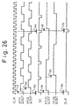
- Figure 25 illustrates a constitution of the divided signal generating circuit according to an embodiment corresponding to the fourth aspect of the present invention
- Fig. 26 shows a timing chart representing the operation thereof.
- the divided signal generating circuit 20a of the present embodiment utilizes the output of the 1/16 frequency-dividing circuit of Fig. 23.
- the circuit 20a includes an OR gate LG 2 which generates a logic sum of the first signal S 1 (output of the OR gate LG 1 ) and the signals at the respective output ends Q of the flip-flops FF 21 , FF 2 2 in the second stage counter JCC 2 and outputs a result thereof as a second signal S 2 (data load pulse DLP).
- reference t F denotes the operation delay time of the flip-flop of one stage
- reference t G denotes the operation delay time of the gate of one stage.
- Figure 27 illustrates a constitution of the 16-bit data demultiplexer circuit according to an embodiment corresponding to the fifth aspect of the present invention
- Fig. 28 shows a timing chart representing the operation thereof.
- Fig. 27 The circuit constitution of Fig. 27 is different from that of Fig. 7 (prior art) in that the divided signal generating circuit 10a (see Fig. 21) is provided in place of the prior art divided signal generating circuit 10b (see Fig. 5). Other constitution is the same as that of Fig. 7 and thus the explanation thereof is omitted.
- the circuit of the present embodiment can produce effects dependent on the embodiments of Figs. 19 and 21.
- Figure 29 illustrates a constitution of the 16-bit data multiplexer circuit according to an embodiment corresponding to the sixth aspect of the present invention
- Fig. 30 shows a timing chart representing the operation thereof.
- Fig. 29 The circuit constitution of Fig. 29 is different from that of Fig. 9 (prior art) in that the divided signal generating circuit 10a (see Fig. 21) is provided in place of the prior art divided signal generating circuit 10b (see Fig. 5). Other constitution is the same as that of Fig. 9 and thus the explanation thereof is omitted. In this embodiment as well, it is possible to obtain effects dependent on the embodiments of Figs. 19 and 21.
- the 1/16 divided signal is obtained using the Johnson-type counters JC 1 , JC 2 (JCC 1 , JCC 2 ) ) of two stages each having two flip-flops
- the ratio of frequency division is not restrictive to 1/16.
- it is possible to arbitrarily select the division ratio by suitably selecting the number of stages of the Johnson-type counter or the number of flip-flops in each counter.
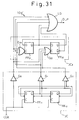
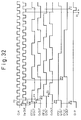
- Figure 31 illustrates a constitution of the divided signal generating circuit according to an embodiment of the present invention, utilizing the counting circuit of Figure 17, and Fig. 32 shows a timing chart representing the operation thereof.
- the divided signal generating circuit 10a' of the present embodiment is different from the divided signal generating circuit 10a shown in Fig. 21 in that the Johnson-type counter JC (see Fig. 17) is provided in place of the Johnson-type counter JC 1 .
- Other constitution is the same as that of Fig. 21 and thus the explanation thereof is omitted.
- each flip-flop FF 11 , FF 1 2 in the first stage counter JC it is possible to increase the operation speed of each flip-flop FF 11 , FF 1 2 in the first stage counter JC, as explained in connection with Figs. 17 and 18. As a result, it is possible to reduce the operation delay time of each flip-flop FF 11 , FF 1 2 and thus heighten a maximum operation frequency of the Johnson-type counter JC. This contributes to a high speed operation of the entire circuit.
- reference t G denotes an operation delay time of each gate of one stage
- reference t F1 denotes an operation delay time of each flip-flop of one stage in the first stage counter JC
- reference t F2 denotes an operation delay time of each flip-flop of one stage in the second stage counter JC 2 .
- Figure 33 illustrates a constitution of the divided signal generating circuit according to another embodiment of the present invention, utilizing the counter circuit of Figure 17, and Fig. 34 shows a timing chart representing the operation thereof.
- the divided signal generating circuit 20a' of the present embodiment is different from the divided signal generating circuit 20a shown in Fig. 25 in that the Johnson-type counter JC (see Fig. 17) is provided in place of the Johnson-type counter JCC 1 .
- Other constitution is the same as that of Fig. 25 and the operation and effects of the entire circuit are easily deduced from the explanation described in connection with Figs. 17 and 18, and thus the explanations thereof are omitted.
- Figures 35 and 36 illustrate constitutions of the 16-bit data demultiplexer circuit and the 16-bit data multiplexer circuit, respectively, as application examples of the divided signal generating circuit 10a' of Fig. 31.
- Respective circuits are different from the corresponding circuits shown in Figs. 27 and 29 in that the divided signal generating circuit 10a' (see Fig. 31) is provided in place of the divided signal generating circuit 10a.
- Other constitutions are the same as those of Figs. 27 and 29 and the operation and effects of the entire circuit are easily deduced from the explanation described in connection with Figs. 17 and 18, and thus the explanations thereof are omitted.
Claims (19)
- Un circuit de compteur comprenant : des compteurs de type Johnson (JC1 ∼ JCm) formant m étages, chaque compteur comprenant un ensemble de bascules (FF11 ∼ FF21 ∼ FF2N2, ... ... FFm1 ∼ FF mNm) connectées en une connexion en cascade, et chaque bascule recevant un signal d'horloge (CLK) sur une borne d'entrée d'horloge (C) respective,
dans lequel des signaux présents sur des bornes de sortie (Q) respectives de toutes les bascules dans un compteur de (k-1)-ième étage, sont appliqués simultanément à chaque borne d'entrée d'horloge (C) de toutes les bascules dans chaque compteur d'un k-ième étage et au-delà, par l'intermédiaire de portes OU respectives. - Un circuit de compteur selon la revendication 1, dans lequel chaque compteur d'un second étage et au-delà comprend une structure de porte (G21, G22) pour recevoir simultanément le signal d'horloge et les signaux provenant des bornes de sortie respectives de bascules dans chaque compteur de l'étage ou des étages précédents.
- Un circuit de génération de signal divisé comprenant : un circuit de compteur selon la revendication 1 ou la revendication 2, et une porte logique (LG) qui génère une somme logique du signal d'horloge et de signaux présents sur des bornes de sortie respectives de toutes les bascules dans le circuit de compteur, et qui fournit en sortie un résultat de cette opération, à titre de m-ième signal (DLP).
- Un circuit de conversion de données, comprenant : un circuit de génération de signal divisé (10, 20) selon la revendication 3,des moyens (11) pour recevoir en entrée des données série (SD) sous la dépendance du signal d'horloge (CLK), et pour convertir les données série en données parallèles (PD) ayant un ensemble de bits; etdes moyens (12) pour mémoriser et fournir en sortie les données parallèles sous la dépendance du m-ième signal (DLP) qui est émis par le circuit de génération de signal divisé.
- Un circuit de conversion de données comprenant : un circuit de génération de signal divisé (10, 20) selon la revendication 3, et des moyens (13) destinés à recevoir en entrée des données parallèles (PD) ayant un ensemble de bits, sous la dépendance du m-ième signal (DLP) qui est fourni par le circuit de génération de signal divisé, et à convertir les données parallèles en données série (SD) sous la dépendance du signal d'horloge (CLK), pour fournir ainsi en sortie les données série converties.
- Un circuit de génération de signal divisé comprenant : un circuit de compteur conforme à la revendication 1 ou la revendication 2, et un compteur de type Johnson du premier étage (JC) comprenant des moyens amplificateurs-séparateurs (G0, G1, G2) pour réguler des instants respectifs auxquels le signal d'horloge et des signaux sur des bornes de sortie respectives de chaque bascule dans le compteur considéré sont appliqués à des bornes d'entrée d'horloge respectives de bascules dans chaque compteur d'un second étage et au-delà, des signaux de sorties non inverseuse et inverseuse d'une bascule du dernier étage (FF12) étant respectivement appliqués à des bornes d'entrée de données inverseuse et non inverseuse d'une bascule du premier étage (FF11), et des niveaux d'amplitude de fonctionnement de signaux de sortie différentiels respectifs des bascules dans le compteur considéré étant fixés de façon à être inférieurs à ceux d'autres circuits.
- Un circuit de génération de signal divisé selon la revendication 6, comprenant en outre une porte logique (LG) qui génère une somme logique du signal d'horloge et de signaux sur des bornes de sortie respectives de toutes les bascules dans le circuit de compteur, et qui fournit en sortie le résultat de cette opération, sous la forme d'un m-ième signal (DLP).
- Circuit de génération de signal divisé selon la revendication 7, dans lequel les moyens amplificateurs-séparateurs comprennent des moyens (G0) pour la régulation de phase, et des moyens (G1, G2) qui sont destinés à recevoir des signaux différentiels respectifs de faible amplitude, provenant de chaque bascule, et à amplifier les signaux différentiels jusqu'à un niveau d'amplitude qui est nécessaire et suffisant pour l'opération logique dans la structure de porte.
- Un circuit démultiplexeur de données comprenant : un circuit de génération de signal divisé (10a') selon la revendication 7 ou la revendication 8; des moyens (FF101 ∼ FF116) pour recevoir en entrée des données série (SD) sous la dépendance du signal d'horloge (CLK, DCLK), et pour convertir les données série en données parallèles (OUT16 ∼ OUT1) ayant un ensemble de bits; et des moyens (FF201 ∼ FF216) pour mémoriser et fournir en sortie les données parallèles sous la dépendance du m-ième signal (DLP) qui est fourni par le circuit de génération de signal divisé.
- Un circuit multiplexeur de données comprenant : un circuit de génération de signal divisé (10a') selon la revendication 7 ou la revendication 8; et des moyens (SEL01 ∼ SEL16, FF301 ∼ FF316) pour recevoir en entrée des données parallèles (D16 ∼ D1) ayant un ensemble de bits, sous la dépendance du m-ième signal (DLP) qui est fourni par le circuit de génération de signal divisé, et pour convertir les données parallèles en données série (OUT) sous la dépendance du signal d'horloge (CLK, DCLK), pour fournir ainsi en sortie les données série converties.
- Un circuit de compteur comprenant : des compteurs de type Johnson (JCC1 ∼ JCCm) formant m étages, chaque compteur comprenant un ensemble de bascules (FF11 ∼ FF21 ∼ FF2N2, ... ... FFm1 ∼ FFmNm) connectées en une connexion en cascade; et (m-1) portes logiques (LG1 ∼ LGm-1), connectées entre chaque étage des compteurs de type Johnson, dans lequel un signal d'horloge (CLK) est appliqué simultanément à des bornes d'entrée d'horloge (C) respectives de bascules dans un compteur de premier étage (JCC1); une somme logique du signal d'horloge et de signaux présents sur des bornes de sortie (Q) respectives de bascules dans le compteur du premier étage est générée par une première porte logique (LG1) et elle est fournie en sortie sous la forme d'un premier signal (S1); le premier signal est appliqué simultanément à des bornes d'entrée d'horloge (C) respectives de bascules dans un compteur de second étage (JCC2); une somme logique du premier signal et des signaux sur des bornes de sortie (Q) respectives de bascules dans le compteur de second étage est générée par une seconde porte logique (LG2), et elle est fournie en sortie sous la forme d'un second signal (S2); et ensuite, d'une manière semblable, un (m-1)-ième signal (Sm-1) est appliqué simultanément à des bornes d'entrée d'horloge (C) respectives de bascules dans un compteur du m-ième étage (JCCm).
- Un circuit de génération de signal divisé comprenant : un circuit de compteur selon la revendication 11; et une porte logique (LGm) qui génère une somme logique du (m-1)-ième signal et de signaux présents sur des bornes de sortie respectives de bascules dans le compteur du m-ième étage, et qui fournit en sortie le résultat de cette opération sous la forme d'un m-ième signal (Sm, DLP).
- Un circuit de conversion de données, comprenant un circuit de génération de signal divisé (10, 20) selon la revendication 12; et des moyens (11) pour recevoir en entrée des données série (SD) sous la dépendance du signal d'horloge (CLK) et pour convertir les données série en données parallèles (PD) ayant un ensemble de bits; et des moyens (12) pour mémoriser et pour fournir en sortie les données parallèles sous la dépendance du m-ième signal (DLP) qui est fourni par le circuit de génération de signal divisé.
- Un circuit de conversion de données comprenant : un circuit de génération de signal divisé (10, 20) selon la revendication 12; et des moyens (13) pour recevoir en entrée des données parallèles (PD) ayant un ensemble de bits, sous la dépendance du m-ième signal (DLP) qui est émis par le circuit de génération de signal divisé, et pour convertir les données parallèles en données série (SD) sous la dépendance du signal d'horloge (CLK), pour fournir ainsi en sortie les données série converties.
- Un circuit de génération de signal divisé comprenant : un circuit de compteur selon la revendication Il; un compteur de type Johnson (JC) d'un premier étage, comprenant des moyens amplificateurs-séparateurs (G0, G1, G2) pour réguler des instants respectifs auxquels le signal d'horloge et des signaux présents sur des bornes de sortie respectives de chaque bascule dans le compteur considéré sont appliqués à la première porte logique, des signaux des sorties non inverseuse et inverseuse d'une bascule du dernier étage (FF12) étant respectivement appliqués à des bornes d'entrée de données inverseuse et non inverseuse d'une bascule du premier étage (FF11), et des niveaux d'amplitude de fonctionnement de signaux de sortie différentiels dans le compteur considéré étant fixés de façon à être inférieurs à ceux d'autres circuits.
- Un circuit de génération de signal divisé selon la revendication 15, comprenant en outre une porte logique (LGm) qui génère une somme logique du (m-1)-ième signal d'horloge et de signaux sur des bornes de sortie respectives de bascules dans le compteur du m-ième étage, et qui fournit en sortie le résultat de cette opération sous la forme d'un m-ième signal (DLP).
- Un circuit de génération de signal divisé selon la revendication 16, dans lequel les moyens amplificateurs-séparateurs comprennent des moyens (G0) pour la régulation de phase, et des moyens (G1, G2) pour recevoir des signaux différentiels respectifs de faible amplitude à partir de chaque bascule et pour amplifier les signaux différentiels jusqu'à un niveau d'amplitude qui est nécessaire et suffisant pour l'opération logique dans la structure de porte.
- Un circuit démultiplexeur de données comprenant un circuit de génération de signal divisé selon la revendication 16; des moyens (FF101 ∼ FF116) pour recevoir en entrée des données série (SD) sous la dépendance du signal d'horloge (CLK, DCLK), et pour convertir les données série en données parallèles (OUT16 ∼ OUT1) ayant un ensemble de bits; et des moyens (FF201 ∼ FF216) pour mémoriser et pour fournir en sortie les données parallèles sous la dépendance du m-ième signal (DLP) qui est fourni par le circuit de génération de signal divisé.
- Un circuit multiplexeur de données comprenant : un circuit de génération de signal divisé selon la revendication 16; et des moyens (SEL01 ∼ SEL16, FF301 ∼ FF316) pour recevoir en entrée des données parallèles (D16 ∼ D1) ayant un ensemble de bits, sous la dépendance du m-ième signal (DLP) qui est fourni par le circuit de génération de signal divisé, et pour convertir les données parallèles en données série (OUT) sous la dépendance du signal d'horloge (CLK, DCLK), pour fournir ainsi en sortie les données série converties.
Priority Applications (1)
| Application Number | Priority Date | Filing Date | Title |
|---|---|---|---|
| EP96203487A EP0766402B1 (fr) | 1991-08-12 | 1992-08-11 | Circuit compteur |
Applications Claiming Priority (4)
| Application Number | Priority Date | Filing Date | Title |
|---|---|---|---|
| JP201771/91 | 1991-08-12 | ||
| JP20177191 | 1991-08-12 | ||
| JP20999192A JP3354597B2 (ja) | 1991-08-12 | 1992-08-06 | カウンタ回路およびその応用回路 |
| JP209991/92 | 1992-08-06 |
Related Child Applications (2)
| Application Number | Title | Priority Date | Filing Date |
|---|---|---|---|
| EP96203487A Division EP0766402B1 (fr) | 1991-08-12 | 1992-08-11 | Circuit compteur |
| EP96203487.2 Division-Into | 1996-12-09 |
Publications (3)
| Publication Number | Publication Date |
|---|---|
| EP0527636A2 EP0527636A2 (fr) | 1993-02-17 |
| EP0527636A3 EP0527636A3 (fr) | 1994-02-09 |
| EP0527636B1 true EP0527636B1 (fr) | 1997-12-29 |
Family
ID=26512981
Family Applications (2)
| Application Number | Title | Priority Date | Filing Date |
|---|---|---|---|
| EP96203487A Expired - Lifetime EP0766402B1 (fr) | 1991-08-12 | 1992-08-11 | Circuit compteur |
| EP92307330A Expired - Lifetime EP0527636B1 (fr) | 1991-08-12 | 1992-08-11 | Circuit compteur utilisant un compteur du type Johnson et son application |
Family Applications Before (1)
| Application Number | Title | Priority Date | Filing Date |
|---|---|---|---|
| EP96203487A Expired - Lifetime EP0766402B1 (fr) | 1991-08-12 | 1992-08-11 | Circuit compteur |
Country Status (5)
| Country | Link |
|---|---|
| US (1) | US5321733A (fr) |
| EP (2) | EP0766402B1 (fr) |
| JP (1) | JP3354597B2 (fr) |
| KR (1) | KR930005374A (fr) |
| DE (2) | DE69223700T2 (fr) |
Families Citing this family (7)
| Publication number | Priority date | Publication date | Assignee | Title |
|---|---|---|---|---|
| US6876717B1 (en) * | 2004-08-19 | 2005-04-05 | Intel Corporation | Multi-stage programmable Johnson counter |
| JP4666462B2 (ja) * | 2005-01-14 | 2011-04-06 | ルネサスエレクトロニクス株式会社 | カウンタ回路と、それを含む半導体装置 |
| JP4965203B2 (ja) * | 2006-09-11 | 2012-07-04 | 株式会社リコー | 遅延時間生成回路、それを用いた二次電池保護用半導体装置、バッテリパックおよび電子機器 |
| US9083994B2 (en) | 2006-09-26 | 2015-07-14 | Qualcomm Incorporated | Method and system for error robust audio playback time stamp reporting |
| KR101121299B1 (ko) * | 2006-11-13 | 2012-03-22 | 콸콤 인코포레이티드 | 고속 시리얼라이저 장치 |
| ATE554529T1 (de) | 2007-10-16 | 2012-05-15 | Austriamicrosystems Ag | Frequenzteiler und verfahren zur frequenzteilung |
| US10837369B2 (en) | 2017-08-23 | 2020-11-17 | General Electric Company | Igniter assembly for a gas turbine combustor |
Family Cites Families (6)
| Publication number | Priority date | Publication date | Assignee | Title |
|---|---|---|---|---|
| US4339722A (en) * | 1979-05-23 | 1982-07-13 | Micro Consultants Limited | Digital frequency multiplier |
| US4519091A (en) * | 1983-08-03 | 1985-05-21 | Hewlett-Packard Company | Data capture in an uninterrupted counter |
| US4685104A (en) * | 1985-02-27 | 1987-08-04 | Srx Corporation | Distributed switching system |
| EP0326856A1 (fr) * | 1988-01-28 | 1989-08-09 | Siemens Aktiengesellschaft | Compteur électronique d'impulsions |
| JP2504568B2 (ja) * | 1989-06-20 | 1996-06-05 | 富士通株式会社 | 信号生成回路 |
| KR0185695B1 (ko) * | 1990-04-27 | 1999-05-01 | 이우에 사또시 | 촬상시스템의 동기회로 |
-
1992
- 1992-08-06 JP JP20999192A patent/JP3354597B2/ja not_active Expired - Lifetime
- 1992-08-11 EP EP96203487A patent/EP0766402B1/fr not_active Expired - Lifetime
- 1992-08-11 DE DE69223700T patent/DE69223700T2/de not_active Expired - Fee Related
- 1992-08-11 DE DE69230480T patent/DE69230480T2/de not_active Expired - Fee Related
- 1992-08-11 EP EP92307330A patent/EP0527636B1/fr not_active Expired - Lifetime
- 1992-08-12 KR KR1019920014524A patent/KR930005374A/ko not_active Application Discontinuation
- 1992-08-12 US US07/928,469 patent/US5321733A/en not_active Expired - Lifetime
Also Published As
| Publication number | Publication date |
|---|---|
| KR930005374A (ko) | 1993-03-23 |
| JP3354597B2 (ja) | 2002-12-09 |
| DE69223700D1 (de) | 1998-02-05 |
| DE69230480D1 (de) | 2000-01-27 |
| EP0527636A2 (fr) | 1993-02-17 |
| EP0766402A2 (fr) | 1997-04-02 |
| US5321733A (en) | 1994-06-14 |
| JPH05191272A (ja) | 1993-07-30 |
| EP0527636A3 (fr) | 1994-02-09 |
| EP0766402A3 (fr) | 1998-01-21 |
| DE69230480T2 (de) | 2000-04-27 |
| DE69223700T2 (de) | 1998-05-07 |
| EP0766402B1 (fr) | 1999-12-22 |
Similar Documents
| Publication | Publication Date | Title |
|---|---|---|
| US6477186B1 (en) | Fast operating multiplexer | |
| EP0404127B1 (fr) | Générateur de signal | |
| EP0527636B1 (fr) | Circuit compteur utilisant un compteur du type Johnson et son application | |
| KR20000017243A (ko) | 펄스폭 변조 파형 발생 회로 | |
| US7436725B2 (en) | Data generator having stable duration from trigger arrival to data output start | |
| US5675271A (en) | Extended chip select reset apparatus and method | |
| KR100272945B1 (ko) | 직병렬데이터변환기 | |
| US7973584B2 (en) | Waveform generator | |
| US7359475B2 (en) | Counter circuit and semiconductor device containing the same | |
| US6686856B1 (en) | Clocking domain conversion system and method | |
| US6091794A (en) | Fast synchronous counter | |
| US6639435B2 (en) | Adjustable frequency divider | |
| JP2690516B2 (ja) | リングカウンタ | |
| JPH0583008B2 (fr) | ||
| JP3145988B2 (ja) | データs/p変換回路 | |
| JP2984429B2 (ja) | 半導体集積回路 | |
| JPH08102658A (ja) | ロード機能付きカウンタ回路 | |
| JPH05175833A (ja) | 位相可変分周回路 | |
| JPH06177722A (ja) | 広範囲遅延生成回路 | |
| JPS63284930A (ja) | mBnB符号変換回路 | |
| JPH0348520B2 (fr) | ||
| JPH04196710A (ja) | デジタル信号遅延回路 | |
| KR960027565A (ko) | 다채널 무선통신 장치에서의 최장 부호열 발생기 | |
| JPH0628151A (ja) | シリアルデータのパラレルラッチ回路 | |
| JPH06276248A (ja) | データフォーマット変換器 |
Legal Events
| Date | Code | Title | Description |
|---|---|---|---|
| PUAI | Public reference made under article 153(3) epc to a published international application that has entered the european phase |
Free format text: ORIGINAL CODE: 0009012 |
|
| AK | Designated contracting states |
Kind code of ref document: A2 Designated state(s): DE FR GB |
|
| PUAL | Search report despatched |
Free format text: ORIGINAL CODE: 0009013 |
|
| AK | Designated contracting states |
Kind code of ref document: A3 Designated state(s): DE FR GB |
|
| 17P | Request for examination filed |
Effective date: 19940804 |
|
| 17Q | First examination report despatched |
Effective date: 19960202 |
|
| GRAG | Despatch of communication of intention to grant |
Free format text: ORIGINAL CODE: EPIDOS AGRA |
|
| GRAH | Despatch of communication of intention to grant a patent |
Free format text: ORIGINAL CODE: EPIDOS IGRA |
|
| GRAH | Despatch of communication of intention to grant a patent |
Free format text: ORIGINAL CODE: EPIDOS IGRA |
|
| GRAA | (expected) grant |
Free format text: ORIGINAL CODE: 0009210 |
|
| AK | Designated contracting states |
Kind code of ref document: B1 Designated state(s): DE FR GB |
|
| XX | Miscellaneous (additional remarks) |
Free format text: TEILANMELDUNG 96203487.2 EINGEREICHT AM 09/12/96. |
|
| REF | Corresponds to: |
Ref document number: 69223700 Country of ref document: DE Date of ref document: 19980205 |
|
| ET | Fr: translation filed | ||
| PLBE | No opposition filed within time limit |
Free format text: ORIGINAL CODE: 0009261 |
|
| STAA | Information on the status of an ep patent application or granted ep patent |
Free format text: STATUS: NO OPPOSITION FILED WITHIN TIME LIMIT |
|
| 26N | No opposition filed | ||
| REG | Reference to a national code |
Ref country code: GB Ref legal event code: IF02 |
|
| PGFP | Annual fee paid to national office [announced via postgrant information from national office to epo] |
Ref country code: DE Payment date: 20080821 Year of fee payment: 17 |
|
| PGFP | Annual fee paid to national office [announced via postgrant information from national office to epo] |
Ref country code: FR Payment date: 20080818 Year of fee payment: 17 |
|
| PGFP | Annual fee paid to national office [announced via postgrant information from national office to epo] |
Ref country code: GB Payment date: 20080820 Year of fee payment: 17 |
|
| GBPC | Gb: european patent ceased through non-payment of renewal fee |
Effective date: 20090811 |
|
| REG | Reference to a national code |
Ref country code: FR Ref legal event code: ST Effective date: 20100430 |
|
| PG25 | Lapsed in a contracting state [announced via postgrant information from national office to epo] |
Ref country code: FR Free format text: LAPSE BECAUSE OF NON-PAYMENT OF DUE FEES Effective date: 20090831 Ref country code: DE Free format text: LAPSE BECAUSE OF NON-PAYMENT OF DUE FEES Effective date: 20100302 |
|
| PG25 | Lapsed in a contracting state [announced via postgrant information from national office to epo] |
Ref country code: GB Free format text: LAPSE BECAUSE OF NON-PAYMENT OF DUE FEES Effective date: 20090811 |