EP0519741B1 - Elément semi-conducteur à haute tension de claquage - Google Patents
Elément semi-conducteur à haute tension de claquage Download PDFInfo
- Publication number
- EP0519741B1 EP0519741B1 EP92305660A EP92305660A EP0519741B1 EP 0519741 B1 EP0519741 B1 EP 0519741B1 EP 92305660 A EP92305660 A EP 92305660A EP 92305660 A EP92305660 A EP 92305660A EP 0519741 B1 EP0519741 B1 EP 0519741B1
- Authority
- EP
- European Patent Office
- Prior art keywords
- layer
- insulation film
- breakdown
- semiconductor active
- semiconductor
- Prior art date
- Legal status (The legal status is an assumption and is not a legal conclusion. Google has not performed a legal analysis and makes no representation as to the accuracy of the status listed.)
- Expired - Lifetime
Links
- 239000004065 semiconductor Substances 0.000 title claims description 31
- 238000009413 insulation Methods 0.000 claims description 43
- 239000000463 material Substances 0.000 claims description 8
- 230000005684 electric field Effects 0.000 description 18
- XUIMIQQOPSSXEZ-UHFFFAOYSA-N Silicon Chemical compound [Si] XUIMIQQOPSSXEZ-UHFFFAOYSA-N 0.000 description 16
- 229910052710 silicon Inorganic materials 0.000 description 16
- 239000010703 silicon Substances 0.000 description 16
- 239000000758 substrate Substances 0.000 description 7
- GWEVSGVZZGPLCZ-UHFFFAOYSA-N Titan oxide Chemical compound O=[Ti]=O GWEVSGVZZGPLCZ-UHFFFAOYSA-N 0.000 description 4
- 230000000694 effects Effects 0.000 description 4
- 230000015556 catabolic process Effects 0.000 description 3
- 239000012774 insulation material Substances 0.000 description 2
- 238000000034 method Methods 0.000 description 2
- VYPSYNLAJGMNEJ-UHFFFAOYSA-N Silicium dioxide Chemical compound O=[Si]=O VYPSYNLAJGMNEJ-UHFFFAOYSA-N 0.000 description 1
- 229910002113 barium titanate Inorganic materials 0.000 description 1
- 238000009792 diffusion process Methods 0.000 description 1
- 238000002955 isolation Methods 0.000 description 1
- 229910052814 silicon oxide Inorganic materials 0.000 description 1
Images


Classifications
-
- H—ELECTRICITY
- H01—ELECTRIC ELEMENTS
- H01L—SEMICONDUCTOR DEVICES NOT COVERED BY CLASS H10
- H01L29/00—Semiconductor devices specially adapted for rectifying, amplifying, oscillating or switching and having potential barriers; Capacitors or resistors having potential barriers, e.g. a PN-junction depletion layer or carrier concentration layer; Details of semiconductor bodies or of electrodes thereof ; Multistep manufacturing processes therefor
- H01L29/40—Electrodes ; Multistep manufacturing processes therefor
- H01L29/408—Electrodes ; Multistep manufacturing processes therefor with an insulating layer with a particular dielectric or electrostatic property, e.g. with static charges or for controlling trapped charges or moving ions, or with a plate acting on the insulator potential or the insulator charges, e.g. for controlling charges effect or potential distribution in the insulating layer, or with a semi-insulating layer contacting directly the semiconductor surface
-
- H—ELECTRICITY
- H01—ELECTRIC ELEMENTS
- H01L—SEMICONDUCTOR DEVICES NOT COVERED BY CLASS H10
- H01L29/00—Semiconductor devices specially adapted for rectifying, amplifying, oscillating or switching and having potential barriers; Capacitors or resistors having potential barriers, e.g. a PN-junction depletion layer or carrier concentration layer; Details of semiconductor bodies or of electrodes thereof ; Multistep manufacturing processes therefor
- H01L29/02—Semiconductor bodies ; Multistep manufacturing processes therefor
- H01L29/06—Semiconductor bodies ; Multistep manufacturing processes therefor characterised by their shape; characterised by the shapes, relative sizes, or dispositions of the semiconductor regions ; characterised by the concentration or distribution of impurities within semiconductor regions
- H01L29/0603—Semiconductor bodies ; Multistep manufacturing processes therefor characterised by their shape; characterised by the shapes, relative sizes, or dispositions of the semiconductor regions ; characterised by the concentration or distribution of impurities within semiconductor regions characterised by particular constructional design considerations, e.g. for preventing surface leakage, for controlling electric field concentration or for internal isolations regions
- H01L29/0607—Semiconductor bodies ; Multistep manufacturing processes therefor characterised by their shape; characterised by the shapes, relative sizes, or dispositions of the semiconductor regions ; characterised by the concentration or distribution of impurities within semiconductor regions characterised by particular constructional design considerations, e.g. for preventing surface leakage, for controlling electric field concentration or for internal isolations regions for preventing surface leakage or controlling electric field concentration
- H01L29/0611—Semiconductor bodies ; Multistep manufacturing processes therefor characterised by their shape; characterised by the shapes, relative sizes, or dispositions of the semiconductor regions ; characterised by the concentration or distribution of impurities within semiconductor regions characterised by particular constructional design considerations, e.g. for preventing surface leakage, for controlling electric field concentration or for internal isolations regions for preventing surface leakage or controlling electric field concentration for increasing or controlling the breakdown voltage of reverse biased devices
- H01L29/0615—Semiconductor bodies ; Multistep manufacturing processes therefor characterised by their shape; characterised by the shapes, relative sizes, or dispositions of the semiconductor regions ; characterised by the concentration or distribution of impurities within semiconductor regions characterised by particular constructional design considerations, e.g. for preventing surface leakage, for controlling electric field concentration or for internal isolations regions for preventing surface leakage or controlling electric field concentration for increasing or controlling the breakdown voltage of reverse biased devices by the doping profile or the shape or the arrangement of the PN junction, or with supplementary regions, e.g. junction termination extension [JTE]
-
- H—ELECTRICITY
- H01—ELECTRIC ELEMENTS
- H01L—SEMICONDUCTOR DEVICES NOT COVERED BY CLASS H10
- H01L29/00—Semiconductor devices specially adapted for rectifying, amplifying, oscillating or switching and having potential barriers; Capacitors or resistors having potential barriers, e.g. a PN-junction depletion layer or carrier concentration layer; Details of semiconductor bodies or of electrodes thereof ; Multistep manufacturing processes therefor
- H01L29/66—Types of semiconductor device ; Multistep manufacturing processes therefor
- H01L29/68—Types of semiconductor device ; Multistep manufacturing processes therefor controllable by only the electric current supplied, or only the electric potential applied, to an electrode which does not carry the current to be rectified, amplified or switched
- H01L29/70—Bipolar devices
- H01L29/72—Transistor-type devices, i.e. able to continuously respond to applied control signals
- H01L29/739—Transistor-type devices, i.e. able to continuously respond to applied control signals controlled by field-effect, e.g. bipolar static induction transistors [BSIT]
- H01L29/7393—Insulated gate bipolar mode transistors, i.e. IGBT; IGT; COMFET
-
- H—ELECTRICITY
- H01—ELECTRIC ELEMENTS
- H01L—SEMICONDUCTOR DEVICES NOT COVERED BY CLASS H10
- H01L29/00—Semiconductor devices specially adapted for rectifying, amplifying, oscillating or switching and having potential barriers; Capacitors or resistors having potential barriers, e.g. a PN-junction depletion layer or carrier concentration layer; Details of semiconductor bodies or of electrodes thereof ; Multistep manufacturing processes therefor
- H01L29/66—Types of semiconductor device ; Multistep manufacturing processes therefor
- H01L29/86—Types of semiconductor device ; Multistep manufacturing processes therefor controllable only by variation of the electric current supplied, or only the electric potential applied, to one or more of the electrodes carrying the current to be rectified, amplified, oscillated or switched
- H01L29/861—Diodes
- H01L29/8611—Planar PN junction diodes
Definitions
- This invention relates to a high-breakdown-voltage semiconductor element.
- a technique of providing a guard ring around an end pn-junction formed in an element region to be supplied with a high voltage is known as a method of increasing the breakdown voltage of a semiconductor element.
- the guard ring reduces the degree of electric field concentration at a tip portion of a depletion layer extending from the pn-junction, thereby increasing the breakdown voltage of the element.
- the effect of reducing the degree of the electric field concentration is obtained by optimally designing the depth of diffusion of the guard ring layer, the distance between the guard ring layer and a terminal region, and the distance between guard ring layers (if a plurality of guard ring layers are employed).
- Fig. 7 shows an end portion of a high-breakdown-voltage diode having such a guard ring structure.
- a high-concentration p-type layer 2 which is to be an anode region, is formed in the upper surface of a high-resistance n-type silicon layer 1 (substrate). Further, a high-concentration n-type layer 3 is formed in the upper surface of the layer 1 separated from the layer 3 by a predetermined distance, for stopping the extension of a depletion layer.
- the layer 3 is provided with an electrode 5 for supplying a voltage identical to that of a cathode.
- High-concentration, p-type layers 21 and 22 serving as guard rings are formed in the surface between the layers 2 and 3.
- An electrode 7 is formed on the lower surface of the layer 1 with a high-concentration n-type layer 6 interposed therebetween.
- the conventional high-breakdown voltage semiconductor element of a guard ring structure is hard to design.
- This invention has been made in consideration of the above circumstances, and aims to provide a high-breakdown-voltage semiconductor element easy to design and having superior high-breakdown-voltage characteristics.
- the present invention provides, a high-breakdown-voltage semiconductor device comprising: a semiconductor active layer having main and back surfaces one on either side; an insulation support layer arranged on the back surface of the semiconductor active layer; a semiconductor support layer arranged on the insulation support layer such that the insulation support layer is interposed between the semiconductor active and semiconductor support layers; a first conductivity-type region and a second conductivity-type region which are formed in the semiconductor active layer along the main surface; and first and second electrodes provided to the semiconductor layer such that they are located one on either side of a junction between the first and second conductivity-type regions, wherein, a first insulation film is interposed between the semiconductor active and insulation support layers, and arranged along the back surface of the semiconductor active layer and between the first and second electrodes, the first insulation film being made of a material having a dielectric constant larger than a material constituting the semiconductor active layer.
- the invention utilizes the characteristic that the state of an electric field caused in the insulation film depends upon conditions given thereto without being influenced by the ambient state, when the dielectric constant of the insulation film is sufficiently large. That is, where an insulation film having a dielectric constant larger than the substrate is provided on the outside of a pn-junction, such as an end one, in an element having a structure as in the invention, a uniform electric field is formed in the insulation film, so that electric field concentration in a region near the insulation film can be avoided when a high reverse bias voltage is applied to the element.
- the invention can provide a high-breakdown-voltage semiconductor element employing an insulation film capable of reducing the degree of electric field concentration caused in that portion of the substrate which is located in the vicinity of the insulation film.
- insulation films made of a material having a dielectric constant larger than that of the substrate is known from EP-A-0 224 968 and JP-A-2 001 980.
- the devices so fabricated are diodes and not transistors.
- Fig. 1 shows a high-breakdown-voltage diode useful in explaining a reduction in the degree of concentration of an electric field by virtue of an insulating film having a large dielectric constant.
- a high-concentration p-type layer 2 serving as an anode terminal is selectively formed in the surface of a high-resistance n-type silicon layer (substrate) 1, and a high-concentration n-type layer 3 for stopping the extension of a depletion layer is formed in the surface, separated from the layer 2 by a predetermined distance.
- An anode electrode 4 and an electrode 5 supply a voltage indentical to that of a cathode are formed on the layers 2 and 3, respectively.
- An insulation film 8 made of TiO 2 and having a dielectric constant larger than that of Si is formed on the upper surface of the n-type silicon layer 1 between the electrodes 4 and 5.
- a cathode electrode 7 is formed on the lower surface of the layer 1 with a high-concentration n-type layer 6 interposed therebetween.
- Fig. 2 shows a state in which a dielectric member A having a dielectric constant ⁇ 1 is in contact with a dielectric member B having a dielectric constant ⁇ 2 .
- the following equation (1) can be obtained by using the Gauss' theorem: n ⁇ ; outward unit vector perpendicular to surface of region ⁇ where Q represents the total charge accumulated in the region ⁇ .
- the equation (1) can be replaced with the following equation (2): where ⁇ 1 represents the dielectric constant of the portion of the region ⁇ 1 on the side of the dielectric member A, ⁇ 2 the dielectric constant of the portion of the region ⁇ 2 on the side of the dielectric member B, and ⁇ the density of charge accumulated in a line extending between a and b .
- Equation (3) is obtained by dividing each side of the equation (2) by ⁇ 2 :
- Equation (5) indicates a condition for a reflection-type boundary. Specifically, where ⁇ 2 is sufficiently larger than ⁇ 1 and than ⁇ l, the internal electric field caused in the region ⁇ 2 of the dielectric member B is determined by only a fixed boundary condition applied to the region, without being affected by the dielectric member A.
- the electric-field concentration-reducing effect of the invention is similar to that of a so-called field plate using a high-resistance film such as an SIPOS.
- the invention is basically different from the field plate in that the former utilizes a uniform electric field formed in the insulation film, while the latter utilizes potential distribution obtained by causing a very small amount of current to flow.
- the dielectric constant of the insulation film must be sufficiently larger than that of silicon as the element material, i.e., be large enough to substantially satisfies the equation (4).
- Figs. 3 to 6 are cross sectional views, showing high-breakdown-voltage diodes according to first to fourth embodiments of the invention.
- like elements are designated by like signs, and duplication of explanation is avoided.
- Fig. 3 shows a first embodiment of the invention, which employs insulation films 13 (13 1 , 13 2 , 13 3 ) having a large dielectric constant.
- the diode according to this embodiment has a dielectric isolation structure obtained, for example, by adhering a second silicon substrate 11 to the first silicon layer 1 with a silicon oxide film 10 interposed therebetween.
- a plurality of insulation films 13 of a large dielectric constant are formed in boundary portions between the silicon layers 1 and 10. The reason why a plurality of insulation films 13 are formed in the diode is that they are not connected to the anode and cathode electrodes 4 and 7.
- the n-type silicon layer 1 becomes a complete depletion layer at the time of applying a reverse bias voltage thereto, the entire voltage is applied to that portion of the depletion layer which extends between the high-concentration p-type layer 2 and high-concentration n-type layer 6.
- the potentials of the insulation films 13, which are in a floating state are determined depending upon the positions thereof, and the degree of electric field in each insulation film 13 is sufficiently lower than in the ambient circumstance. Accordingly, in a bottom portion of the silicon layer 1, the potential varies in stepwise such that it is flattened in the insulation films 13 in the horizontal direction. Thus, concentration of an electric field caused in the insulation films 13 by the influence of the side of the substrate 11 is relaxed, thereby providing high-breakdown-voltage characteristics.
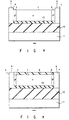
- Fig. 4 shows a second embodiment of the invention which employs an insulation film 13 formed on the over all lower surface of the n-type silicon layer 1.
- the both opposite ends of the insulation film 13 are connected to an anode electrode 4 and a cathode electrode 7 which extend to the bottom of the element.
- concentration of an electric field in a lower portion of the layer 1 is relaxed.
- Fig. 5 shows a third embodiment which is a substantial combination of the structures shown in Figs. 1 and 4.
- insulation films 8 and 13 of a large dielectric constant are formed on the lower and upper surfaces of an end portion of the n-type silicon layer 1, respectively, thereby providing a diode having a higher breakdown voltage.
- Fig. 6 shows a fourth embodiment which is a combination of the structures of Figs 1 and 3. This embodiment also provides superior high-breakdown-voltage characteristics.
Landscapes
- Engineering & Computer Science (AREA)
- Microelectronics & Electronic Packaging (AREA)
- Power Engineering (AREA)
- Physics & Mathematics (AREA)
- Ceramic Engineering (AREA)
- Condensed Matter Physics & Semiconductors (AREA)
- General Physics & Mathematics (AREA)
- Computer Hardware Design (AREA)
- Electrodes Of Semiconductors (AREA)
- Insulated Gate Type Field-Effect Transistor (AREA)
- Element Separation (AREA)
Claims (7)
- Dispositif semiconducteur à tension de rupture élevée comprenant:une couche semiconductrice active (1) comportant des surfaces principale et arrière, une surface étant agencée sur chaque côté correspondant;une couche de support d'isolation (10) agencée sur la surface arrière de la couche semiconductrice active (1);une couche semiconductrice de support (11), agencée sur la couche de support d'isolation(10), la couche de support d'isolation étant ainsi interposée entre la couche semiconductrice active et la couche semiconductrice de support (1, 11);une région du premier type de conductivité (2) et une région du deuxième type de conductivité (6), formées dans la couche semiconductrice active (1) le long de la surface principale; etdes première et deuxième électrodes (4, 7), agencées par rapport à la couche semiconductrice (1) de sorte qu'une électrode se situe de chaque côté d'une jonction pn entre les régions des premier et deuxième types de conductivité (2, 6);caractérisé en ce qu'un premier film d'isolation (13) est interposé entre la couche semiconductrice active et la couche de support d'isolation (1, 10) et agencé le long de la surface arrière de la couche semiconductrice active (1) ainsi qu'entre les première et deuxième électrodes (4, 7), le premier film d'isolation (13) étant composé d'un matériau ayant une constante diélectrique supérieure à celle d'un matériau composant la couche semiconductrice active (1).
- Dispositif selon la revendication 1, caractérisé en ce que les première et deuxième électrodes (4, 7) sont respectivement en contact avec les régions des premier et deuxième types de conductivité (2, 6).
- Dispositif selon les revendications 1 ou 2, caractérisé en ce que le premier film d'isolation (13) est en contact avec les première et deuxième électrodes (4, 7)
- Dispositif selon les revendications 1 ou 2, caractérisé en ce que le premier film d'isolation (13) est composé de plusieurs parties (131, 132, 133), séparées les unes des autres.
- Dispositif selon l'une quelconque des revendications 1 à 4, caractérisé en ce que la couche semiconductrice active (1) est d'un premier type de conductivité présentant une résistance élevée.
- Dispositif selon l'une quelconque des revendications 1 à 5, caractérisé en ce que le deuxième film d'isolation (8) est agencé le long de la surface principale de la couche semiconductrice active et entre les première et deuxième électrodes (4, 7), le deuxième film d'isolation (8) étant composé d'un matériau ayant une constante diélectrique supérieure à celle du matériau composant la couche semiconductrice active (1).
- Dispositif selon la revendication 6, caractérisé en ce que le deuxième film d'isolation (8) est en contact avec les première et deuxième électrodes (4, 7).
Applications Claiming Priority (2)
| Application Number | Priority Date | Filing Date | Title |
|---|---|---|---|
| JP15057691 | 1991-06-21 | ||
| JP150576/91 | 1991-06-21 |
Publications (3)
| Publication Number | Publication Date |
|---|---|
| EP0519741A2 EP0519741A2 (fr) | 1992-12-23 |
| EP0519741A3 EP0519741A3 (en) | 1993-05-19 |
| EP0519741B1 true EP0519741B1 (fr) | 1997-05-02 |
Family
ID=15499908
Family Applications (1)
| Application Number | Title | Priority Date | Filing Date |
|---|---|---|---|
| EP92305660A Expired - Lifetime EP0519741B1 (fr) | 1991-06-21 | 1992-06-19 | Elément semi-conducteur à haute tension de claquage |
Country Status (3)
| Country | Link |
|---|---|
| US (1) | US5323041A (fr) |
| EP (1) | EP0519741B1 (fr) |
| DE (1) | DE69219405T2 (fr) |
Families Citing this family (11)
| Publication number | Priority date | Publication date | Assignee | Title |
|---|---|---|---|---|
| US5597758A (en) * | 1994-08-01 | 1997-01-28 | Motorola, Inc. | Method for forming an electrostatic discharge protection device |
| US5701023A (en) * | 1994-08-03 | 1997-12-23 | National Semiconductor Corporation | Insulated gate semiconductor device typically having subsurface-peaked portion of body region for improved ruggedness |
| DE19820956A1 (de) * | 1998-05-11 | 1999-11-18 | Daimler Chrysler Ag | Halbleiter-Bauelement und Verfahren zu seiner Herstellung sowie Verwendung des Halbleiter-Bauelements |
| SE9904710L (sv) * | 1999-12-22 | 2001-06-23 | Abb Ab | Halvledaranordning |
| SE0003360D0 (sv) * | 2000-09-21 | 2000-09-21 | Abb Ab | A semiconductor device |
| US7071537B2 (en) * | 2002-05-17 | 2006-07-04 | Ixys Corporation | Power device having electrodes on a top surface thereof |
| DE10316222B3 (de) * | 2003-04-09 | 2005-01-20 | eupec Europäische Gesellschaft für Leistungshalbleiter mbH | Verfahren zur Herstellung eines robusten Halbleiterbauelements und damit hergestelltes Halbleiterbauelement |
| KR20060013397A (ko) | 2003-05-13 | 2006-02-09 | 코닌클리즈케 필립스 일렉트로닉스 엔.브이. | 전계 형성 영역을 구비한 반도체 장치 |
| JP2008544535A (ja) | 2005-06-22 | 2008-12-04 | エヌエックスピー ビー ヴィ | 絶縁破壊電圧が相対的に高い半導体デバイス及びその製造方法 |
| WO2010046794A1 (fr) | 2008-10-20 | 2010-04-29 | Nxp B.V. | Dispositif à semi-conducteurs et son procédé de fabrication |
| KR101652403B1 (ko) * | 2010-08-13 | 2016-08-31 | 삼성전자주식회사 | 전력 전자소자 및 그 제조방법 |
Family Cites Families (9)
| Publication number | Priority date | Publication date | Assignee | Title |
|---|---|---|---|---|
| US3686544A (en) * | 1969-02-10 | 1972-08-22 | Philips Corp | Mosfet with dual dielectric of titanium dioxide on silicon dioxide to prevent surface current migration path |
| US4388635A (en) * | 1979-07-02 | 1983-06-14 | Hitachi, Ltd. | High breakdown voltage semiconductor device |
| DE2944937A1 (de) * | 1979-11-07 | 1981-06-04 | Siemens AG, 1000 Berlin und 8000 München | Halbleiterbauelement |
| US4890150A (en) * | 1985-12-05 | 1989-12-26 | North American Philips Corporation | Dielectric passivation |
| JP2585331B2 (ja) * | 1986-12-26 | 1997-02-26 | 株式会社東芝 | 高耐圧プレーナ素子 |
| US4799100A (en) * | 1987-02-17 | 1989-01-17 | Siliconix Incorporated | Method and apparatus for increasing breakdown of a planar junction |
| USH665H (en) * | 1987-10-19 | 1989-08-01 | Bell Telephone Laboratories, Incorporated | Resistive field shields for high voltage devices |
| US4927772A (en) * | 1989-05-30 | 1990-05-22 | General Electric Company | Method of making high breakdown voltage semiconductor device |
| JPH0473970A (ja) * | 1990-07-16 | 1992-03-09 | Fuji Electric Co Ltd | Mos型半導体装置 |
-
1992
- 1992-06-19 US US07/901,111 patent/US5323041A/en not_active Expired - Lifetime
- 1992-06-19 EP EP92305660A patent/EP0519741B1/fr not_active Expired - Lifetime
- 1992-06-19 DE DE69219405T patent/DE69219405T2/de not_active Expired - Lifetime
Non-Patent Citations (1)
| Title |
|---|
| International Electron Devices Meeting, IEDM '87, pages 778 - 781 * |
Also Published As
| Publication number | Publication date |
|---|---|
| EP0519741A3 (en) | 1993-05-19 |
| DE69219405T2 (de) | 1997-09-11 |
| EP0519741A2 (fr) | 1992-12-23 |
| US5323041A (en) | 1994-06-21 |
| DE69219405D1 (de) | 1997-06-05 |
Similar Documents
| Publication | Publication Date | Title |
|---|---|---|
| US4686551A (en) | MOS transistor | |
| US4422089A (en) | Semiconductor device having a reduced surface field strength | |
| US6624472B2 (en) | Semiconductor device with voltage sustaining zone | |
| US20030160281A1 (en) | Semiconductor high-voltage devices | |
| US20010050375A1 (en) | Semiconductor device | |
| EP0165644B1 (fr) | Dispositif semi-conducteur à tension de claquage | |
| JPS6338867B2 (fr) | ||
| EP0809864B1 (fr) | Dispositif soi a couche mince laterale a oxyde de champ a gradation lineaire et profil de dopage lineaire | |
| US4908682A (en) | Power MOSFET having a current sensing element of high accuracy | |
| JPH0582070B2 (fr) | ||
| GB2089119A (en) | High voltage semiconductor devices | |
| US6344676B1 (en) | Power semiconductor device having low on-resistance and high breakdown voltage | |
| EP0519741B1 (fr) | Elément semi-conducteur à haute tension de claquage | |
| CA1121516A (fr) | Mosfet de puissance | |
| KR100256387B1 (ko) | 수평 절연 게이트 반도체 장치 | |
| EP0071335B1 (fr) | Transistor à effet de champ | |
| US4047196A (en) | High voltage semiconductor device having a novel edge contour | |
| EP1038308B1 (fr) | Dispositif lateral soi à couche mince | |
| EP0077337A1 (fr) | Transistor de puissance mos | |
| KR19990087140A (ko) | 반도체 소자 | |
| US5229634A (en) | Vertical power mosfet | |
| EP0110320B1 (fr) | Transistor de type MOS | |
| US4890150A (en) | Dielectric passivation | |
| US5504360A (en) | Vertical type semiconductor device provided with an improved construction to greatly decrease device on-resistance without impairing breakdown | |
| EP1202352B1 (fr) | Dispositif semiconducteur à tension de claquage élevée |
Legal Events
| Date | Code | Title | Description |
|---|---|---|---|
| PUAI | Public reference made under article 153(3) epc to a published international application that has entered the european phase |
Free format text: ORIGINAL CODE: 0009012 |
|
| 17P | Request for examination filed |
Effective date: 19920713 |
|
| AK | Designated contracting states |
Kind code of ref document: A2 Designated state(s): CH DE IT LI |
|
| PUAL | Search report despatched |
Free format text: ORIGINAL CODE: 0009013 |
|
| AK | Designated contracting states |
Kind code of ref document: A3 Designated state(s): CH DE IT LI |
|
| 17Q | First examination report despatched |
Effective date: 19950323 |
|
| GRAG | Despatch of communication of intention to grant |
Free format text: ORIGINAL CODE: EPIDOS AGRA |
|
| GRAH | Despatch of communication of intention to grant a patent |
Free format text: ORIGINAL CODE: EPIDOS IGRA |
|
| GRAH | Despatch of communication of intention to grant a patent |
Free format text: ORIGINAL CODE: EPIDOS IGRA |
|
| RBV | Designated contracting states (corrected) |
Designated state(s): DE |
|
| GRAA | (expected) grant |
Free format text: ORIGINAL CODE: 0009210 |
|
| AK | Designated contracting states |
Kind code of ref document: B1 Designated state(s): DE |
|
| REF | Corresponds to: |
Ref document number: 69219405 Country of ref document: DE Date of ref document: 19970605 |
|
| PLBE | No opposition filed within time limit |
Free format text: ORIGINAL CODE: 0009261 |
|
| STAA | Information on the status of an ep patent application or granted ep patent |
Free format text: STATUS: NO OPPOSITION FILED WITHIN TIME LIMIT |
|
| 26N | No opposition filed | ||
| PGFP | Annual fee paid to national office [announced via postgrant information from national office to epo] |
Ref country code: DE Payment date: 20110615 Year of fee payment: 20 |
|
| REG | Reference to a national code |
Ref country code: DE Ref legal event code: R071 Ref document number: 69219405 Country of ref document: DE |
|
| REG | Reference to a national code |
Ref country code: DE Ref legal event code: R071 Ref document number: 69219405 Country of ref document: DE |
|
| PG25 | Lapsed in a contracting state [announced via postgrant information from national office to epo] |
Ref country code: DE Free format text: LAPSE BECAUSE OF EXPIRATION OF PROTECTION Effective date: 20120620 |