EP0511005B1 - Bildaufnahmegerät mit Taktimpulserzeugung nach Wahl - Google Patents
Bildaufnahmegerät mit Taktimpulserzeugung nach Wahl Download PDFInfo
- Publication number
- EP0511005B1 EP0511005B1 EP92303720A EP92303720A EP0511005B1 EP 0511005 B1 EP0511005 B1 EP 0511005B1 EP 92303720 A EP92303720 A EP 92303720A EP 92303720 A EP92303720 A EP 92303720A EP 0511005 B1 EP0511005 B1 EP 0511005B1
- Authority
- EP
- European Patent Office
- Prior art keywords
- clock pulse
- signal
- image pickup
- image
- output
- Prior art date
- Legal status (The legal status is an assumption and is not a legal conclusion. Google has not performed a legal analysis and makes no representation as to the accuracy of the status listed.)
- Expired - Lifetime
Links
Images



Classifications
-
- H—ELECTRICITY
- H04—ELECTRIC COMMUNICATION TECHNIQUE
- H04N—PICTORIAL COMMUNICATION, e.g. TELEVISION
- H04N9/00—Details of colour television systems
- H04N9/79—Processing of colour television signals in connection with recording
- H04N9/80—Transformation of the television signal for recording, e.g. modulation, frequency changing; Inverse transformation for playback
- H04N9/81—Transformation of the television signal for recording, e.g. modulation, frequency changing; Inverse transformation for playback the individual colour picture signal components being recorded sequentially only
-
- H—ELECTRICITY
- H04—ELECTRIC COMMUNICATION TECHNIQUE
- H04N—PICTORIAL COMMUNICATION, e.g. TELEVISION
- H04N25/00—Circuitry of solid-state image sensors [SSIS]; Control thereof
-
- H—ELECTRICITY
- H04—ELECTRIC COMMUNICATION TECHNIQUE
- H04N—PICTORIAL COMMUNICATION, e.g. TELEVISION
- H04N5/00—Details of television systems
- H04N5/76—Television signal recording
- H04N5/765—Interface circuits between an apparatus for recording and another apparatus
- H04N5/77—Interface circuits between an apparatus for recording and another apparatus between a recording apparatus and a television camera
- H04N5/772—Interface circuits between an apparatus for recording and another apparatus between a recording apparatus and a television camera the recording apparatus and the television camera being placed in the same enclosure
Definitions
- the present invention relates to an image pickup apparatus, and particularly to an image pickup apparatus having a solid-state image pickup element and a memory.
- a memory controller for controlling the memory is provided with a clock generation circuit to drive the solid-state image pickup element based on the clock of the clock generation circuit or to perform the signal processing.
- a video camera in which the clock pulse is independently generated in the memory controller and a timing generator is provided for driving the solid-state image pickup element.
- the clock is possibly modulated by the frequency component of the pulse generated in the memory controller, and the driving pulse for the solid-state image pickup element and the pulse for use in the signal processing are generated by the timing generator using this clock, so that the driving pulse or the signal processing pulse which is a high speed pulse inherited modulated components of the clock, and is superimposed as the noise on a video signal output from the solid-state image pickup element or a video signal within the signal processing circuit.
- the driving pulse or the signal processing pulse which is a high speed pulse inherited modulated components of the clock, and is superimposed as the noise on a video signal output from the solid-state image pickup element or a video signal within the signal processing circuit.
- JP-A-3070277 discloses an image pickup apparatus comprising:
- an image pickup apparatus comprising:
- an image processing apparatus comprising:
- the present invention provides an image pickup method comprising the steps of:
- the present invention provides an image processing method comprising the steps of:
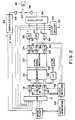
- Fig. 1 is a block diagram showing an image pickup apparatus according to one embodiment of the present invention.
- Fig. 1, 1 is a clock pulse generation circuit useful to generate the clock pulse having a predetermined clock pulse, when a solid-state image pickup element 6 is operating.
- 2 is a timing generator (thereinafter abbreviated TG) for generating the pulse necessary for a camera signal processing circuit 7, and having a pulse generation circuit 2a inside thereof.
- 3 is a signal generator (thereinafter abbreviated SSG) for generating the pulse necessary for each portion of the image pickup device in this embodiment, having a change-over switch 17 and a pulse generation circuit 3a.
- the change-over switch 17 is a switch for changing selectively the clock pulse from one of the clock pulse generation circuits 1, 5 to the other, in which the pulse generation circuit 3a generates the pulse based on the clock pulse selected.
- the 4 is a memory controller for controlling the memory 100, having a change-over switch 180 and a pulse generation circuit 4a inside thereof.
- the change-over switch 180 is a switch for changing the clock pulse from one of the clock pulse generation circuits 1, 5 to the other, in the same way as previously described, in which the pulse generation circuit 4a generates the pulse based on the clock pulse set by the change-over switch 180.
- 5 is a clock pulse generation circuit useful to generate the clock pulse having a predetermined frequency, when the solid-state image pickup element 6 is not operating.
- 6 is a solid-state image pickup element consisting of a CCD image sensor
- 7 is a camera signal processing circuit for processing a signal read from the solid-state image pickup element 6 into a predetermined signal format
- 8 is a switch for switching between the camera signal processing circuit 7 and a reproduction processing circuit 16 as will be described later
- 9 is an A/D converter for converting an input signal from the circuit switched by the switch 8 into the digital signal.
- 100 is a memory for storing a video signal
- 11 is a D/A converter for converting the digital signal into the analog signal in reading the video signal stored in the memory 100
- 120 is a switch for connecting the output of the D/A converter 11 to an external output signal processing circuit 13 or a recording processing circuit 140.
- the external output signal processing circuit 13 is a circuit for processing the video signal into a predetermined signal format in outputting it to the outside
- the recording processing circuit 140 is a circuit for processing the video signal into a predetermined signal format in recording it on a recording medium 15.
- 160 is a reproduction processing circuit for processing the reproduction signal into a predetermined signal format in reproducing the signal stored in the recording medium 15.
- 19 is a system controller for controlling the change-over of the switches 8, 12, 17 and 180, as above described, appropriately in accordance with the operation of an operation key.
- the switch 8 is connected to the a side.
- An image pixel signal of the solid-state image pickup element 6 is converted into the digital signal by the A/D converter 9, after being subjected to a predetermined process of the camera signal processing circuit 7, and stored in the memory 100.
- TG2 generates the driving pulse of the solid-state image pickup element 6 and the signal processing pulse, based on the clock pulse generated by the clock pulse generation circuit 1, which are then output into the solid-state image pickup element 6 and the camera signal processing circuit 7, respectively.
- the solid-state image pickup element 6 and the camera signal processing circuit 7 are driven by the pulse signal generated in the pulse generation circuit 2a based on the clock pulse generated in the clock pulse generation circuit 1.
- the switches 17 and 180 provided inside the SSG3 and the memory controller 4 are switched to the respective a sides.
- the pulse generation circuits in the SSG3 and the memory controller 4 generate respective pulses, based on the clock pulse of the clock pulse generation circuit 1, which are then sent out to related portions. Accordingly, when the solid-state image pickup element 6 is operating, all the processing is performed based on the clock pulse generated in the clock pulse generation circuit 1.
- the switch 8 when the switch 8 is changed to the b side, or when by reading out the signal stored in the memory 100, the video signal is output to the outside, or the signal is recorded on the recording medium 15, the switches 17 and 180 in the SSG3 and the memory controller 4 are connected to the respective b sides.
- the pulse generation circuits of the SSG3 and the memory controller 4 generate respective pulses based on the clock pulse generated in the clock pulse generation circuit 5 and output them to related portions. Accordingly, when the solid-state image pickup element 6 is not operating, all the processing is performed based on the clock pulse generated in the clock puse generation circuit 5.
- Fig. 2 is a configuration block diagram of another embodiment of the present invention.
- 10 is an image pickup element for making the photoelectric conversion of an object image and outputting an RGB image signal
- 12 is an analog switch
- 14, 16, 18 are A/D converters for converting an analog signal from the analog switch 12 into the digital signal
- 20 is a memory having the memory capacity as large as at least one picture
- 22 is a digital signal processing circuit for making the gamma correction, the conversion into a luminance/color difference signal, the addition of a synchronizing signal and the aperture compensation, for an output signal of the image pickup element 10, and the line coincidence of a color difference line sequential signal, the drop-out compensation and the interlace, for a reproduced signal from the recording medium, whereby this circuit outputs a luminance signal Y and two color difference signals R-Y, B-Y, irrespective of the input signal format.
- 24, 26, 28 are D/A converters for converting three digital outputs of the digital signal processing circuit 22 into respective analog signals
- 30, 32, 34 are low
- 36 is a modification circuit for FM modulating the outputs of the LPFs 30, 32, 34 to the frequency band appropriate for recording onto a recording medium such as a magnetic disk
- 38 is a recording amplifier
- 40 is a change-over switch for switching between the recording and the reproduction
- 42 is a magnetic head.
- 44 is a reproduction amplifier for amplifying the reproduced output of the magnetic head 42
- 46 is a demodulation circuit for demodulating the output of the reproduction amplifier 44.
- the interface 48 is a color encoder for generating a composite video signal in the standard format from the outputs of the LPFs 30, 32, 34, i.e., a luminance signal Y and color difference signals R-Y, B-Y, the generated composite video signal being output from an output terminal 50 to the outside.
- 52 is an interface for outputting the digital signals of the A/D converters 14, 16, 18 to the outside, and 54 is a digital output terminal for the connection to the external apparatus.
- the interface 52 comprises a compression circuit or an error detection/correction encoding circuit, if necessary.
- the A/D converters 14, 16, 18 and the D/A converters 24, 26, 28, and 58 is a clock switching circuit for switching the frequencies of sampling clocks ⁇ 0, ⁇ 1, ⁇ 2, ⁇ 3, ⁇ 4, ⁇ 5 supplied from the clock generation circuit 56 to the A/D converters 14, 16, 18 and the D/A converters 24, 26, 28, in accordance with operation mode.
- the analog switch l2 allows for the selection of the output (RGB) of the image pickup element 10, the output (luminance signal Y and line sequential color difference signals R-Y/B-Y) of the demodulation circuit 46, or the output (luminance signal Y and color difference signals R-Y/B-Y) of the LPFs 30, 32, 34.
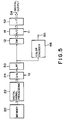
- a recording mode for recording a photographed image with the image pickup element 10 onto a recording medium, not shown, a reproduction output mode for outputting a reproduced image from the recording medium, not shown, in the composite or digital output form, and a still picture output mode for outputting an image (a photographed image with the image pickup element 10 or a still picture reproduced from the recording medium) stored in the memory 20 in the composite or digital output form are provided, and the block diagram reconfigured from the block diagram of Fig. 2 in accordance with the flow of the luminance signal in each mode is shown in Figs. 3, 4 and 5.
- the analog switch 12 selects the RGB output of the image pickup element 10 and applies it to the A/D converters 14, 16, 18.
- the clock switching circuit 58 supplies the sampling clocks ⁇ 0, ⁇ 1, ⁇ 2 having a frequency f0 appropriate for sampling the output of the image pickup element 10 to the A/D converters 14, 16, 18, respectively, and supplies the sampling clocks ⁇ 3, ⁇ 4, ⁇ 5 having a frequency f1 corresponding to the sampling frequency f0 in the A/D converters 14, 16, 18 to the D/A converters 24, 26, 28, respectively.
- a switch 40 is connected to the side of the recording amplifier 38.
- the RGB image signal of an object image with the image pickup element 10 is applied via the analog switch 12 to the A/D converters 14, 16, 18.
- the RGB signal digitized by the A/D converters 14, 16, 18 is stored in the memory 20, and the digital signal processing circuit 22 makes the gamma correction, the conversion into the luminance/color difference signal, the addition of a synchronizing signal, and the aperture compensation for the image data on the memory 20, and outputs an image signal in the form of a luminance signal Y and color difference signals R-Y, B-Y, in which the D/A converters 24, 26, 28 convert the luminance signal Y and the color difference signals R-Y and B-Y into analog signals.
- the outputs of the D/A converters 24, 26, 28 are limited in a certain band by the LPFs 30, 32, 34, and applied to the modulation circuit 36 to modulate them.
- the output of the modulation circuit 36 is applied via the recording amplifier and the switch 40 to the magnetic head, and recorded on a recording medium, not shown.
- the outputs of the LPFs 30, 32, 34 are also applied to a color encoder 48, converted into a composite video signal, and supplied via a video output terminal 50 to an external monitor. Thus, a photographed image to be recorded can be confirmed visually.
- the analog switch 12 selects the output of the demodulation circuit 46 to be applied to the A/D converters 14, 16, 18.
- the clock switching circuit 58 supplies the sampling clocks ⁇ 0, ⁇ 1, ⁇ 2 having a frequency f1, with the aspect ratio of pixel being 1 to 1, to the A/D converters 14, 16, 18, and supplies the sampling clocks ⁇ 3, ⁇ 4, ⁇ 5 having a frequency f3 for converting an image data sampled at a sampling frequency f1 in the A/D converters 14, 16, 18 into analog component signal to the D/A converters 24, 26, 28.
- the switch 40 is connected to the side of the reproduction amplifier 44.
- the output of the magnetic head 42 is applied via the switch 40 and the reproduction amplifier 44 to the demodulation circuit 46.
- the demodulation circuit 46 outputs a reproduction image signal in the form of the luminance signal Y and the line sequential color difference signal R-Y/B-Y, and the analog switch 12 applies two output signals of the demodulation circuit 46 to, for example, the A/D converters 14, 16.
- the A/D converters 14, 16 sample and digitize the output of the demodulation circuit 46 at a sampling frequency, with the aspect ratio of pixel being 1 to 1, and write the output data in the memory 20, which data is output via an interface 52 to a digital output terminal 54.
- the digital luminance signal Y and the digital line sequential color difference signal R-Y/B-Y with the aspect ratio of pixel being 1 to 1, can be obtained via the digital output terminal 54.
- the digital signal processing circuit 22 makes the line coincidence of the color difference line sequential signal, the drop out compensation, and the interlace for reproduced image data stored in the memory 20, and outputs the digital luminance signal Y and the digital color difference signals R-Y, B-Y of the line coincidence.
- the D/A converters 24, 26, 28 convert the outputs of the digital signal processing circuit 22 into analog signals at the same clock frequency as the sampling frequency of the A/D converters 14, 16, which signals are limited in certain bands by the LPFs 30, 32, 34, respectively, converted into a composite video signal by the color encoder 48 and output via a composite output terminal 50.
- the analog switch 12 selects the output of the LPFs 30, 32, 34 to be applied to the A/D converters 14, 16, 18.
- the clock switching circuit 58 supplies the sampling clocks ⁇ 0, ⁇ 1, ⁇ 2 having a frequency f1 to the A/D converters 14, 16, 18, and supplies the sampling clocks ⁇ 3, ⁇ 4, ⁇ 5 having a frequency f2 to the D/A converters 24, 26, 28.
- the image data stored in the memory 20 is read and applied as the luminance signal Y and the color difference signals R-Y and B-Y through the digital signal processing circuit 22 to the D/A converters 24, 26, 28.
- the D/A converters 24, 26, 28 convert the luminance signal Y, the color difference signal R-Y and the color difference signal B-Y into analog signal.
- the outputs of the D/A converters 24, 26, 28 are limited in certain bands by the LPFs 30, 32, 34, converted into a composite video signal by the color encoder 48, and supplied via the video output terminal 50 to an external monitor.
- the composite video signal for an image stored in memory 20 can be obtained.
- the outputs of the LPFs 30, 32, 34 are also applied via the analog switch 12 to the A/D converters 14, 16, 18. Since the sampling frequency of the A/D converters 14, 16, 18 is set at a frequency f1, with the aspect ratio of pixel being 1 to 1, the image data output from the A/D converters 14, 16, 18 have an aspect ratio of pixel of 1 to 1.
- the interface 52 outputs the output data of the A/D converters 14, 16, 18 to the digital output terminal 54.
- the following action must be taken in the reproduction output mode and the still picture output mode.
- the frequencies of the sampling clocks for the A/D converters 14, 16, 18 and the D/A converters 24, 26, 28 must be two-thirds of f1 and f3, respectively.
- the frequency of the sampling clocks for the D/A converters 24, 26, 28 remains f2
- the frequency of the sampling clocks for the A/D converters 14, 16, 18 must be two-thirds of f1.
- the image pickup element 10 outputs an image signal in the RGB format, but it will be appreciated that the image signal can be output in complementary colors or other combination.
- the digital signal processing is not required by the digital signal processing circuit 22, the signal will bypass or simply pass through the digital signal processing circuit 22.
- the output from the digital interface is in the form of Y, R-Y and B-Y in the above described embodiment, but it will be appreciated that it may be in other form such as RGB.
- the present invention can provide the output of a digital image having a desired sampling rate or aspect ratio without the addition of A/D converting means.
- the aspect ratio of pixel is often 1 to 1, so that when a photographed image is transferred to the computer, it is preferable to output the digital data at an aspect ratio of 1 to 1. Also, when a hard copy is made with the printer, it is desirable to output the digital data at an aspect ratio of pixel in accordance with a dot pitch of the printer.
- the aspect ratio of pixel for the digital output is a fixed value corresponding to the aspect ratio of pixel in an image pickup element for use, whereby it is necessary to change the aspect ratio of pixel on the side of a computer or printer, causing a problem with the connectability to the computer or the processing load for changing the aspect ratio.
- this embodiment it is possible to pick up the image data at a desired sampling rate or aspect ratio via digital interface means because of the ability of selecting freely the sampling clock frequencies for the A/D converting means and the D/A converting means, as well as providing the digital output of reproduced image data at a desired sampling rate or aspect ratio through an image reproduction device which passes the reproduced image signal into the selecting means.
Landscapes
- Engineering & Computer Science (AREA)
- Multimedia (AREA)
- Signal Processing (AREA)
- Television Signal Processing For Recording (AREA)
Claims (10)
- Bildaufnahmegerät mit:(a) einer eine Bildaufnahmeeinrichtung (6) aufweisenden Signalverarbeitungseinrichtung (6,7),(b) einer ersten Taktimpulserzeugungseinrichtung (1, 2, 2a) zur Erzeugung eines ersten Taktimpulses mit einer ersten vorbestimmten Frequenz,(c) einer zweiten Taktimpulserzeugungseinrichtung (4, 4a, 5) zur Erzeugung eines zweiten Taktimpulses mit einer zweiten vorbestimmten Frequenz, und(d) Schalteinrichtungen (17, 180) zur wahlweisen Zufuhr des Ausgangssignals der ersten Taktimpulserzeugungseinrichtung (1, 2, 2a) oder der zweiten Taktimpulserzeugungseinrichtung (4, 4a, 5) zu der Signalverarbeitungseinrichtung (6,7);gekennzeichnet durch
(e) eine Steuerungseinrichtung (19) zur Steuerung des Schaltens der Schalteinrichtungen (17, 180), so daß der erste Taktimpuls der Signalverarbeitungseinrichtung (6,7) zugeführt wird, wenn die Bildaufnahmeeinrichtung (6) in Betrieb ist und der zweite Taktimpuls der Signalverarbeitungseinrichtung (6,7) zugeführt wird, wenn die Bildaufnahmeeinrichtung (6) nicht in Betrieb ist. - Bildaufnahmegerät nach Anspruch 1,
gekennzeichnet durcheine Speichereinrichtung (100) zur Speicherung des Ausgangssignals der Bildaufnahmeeinrichtung (6), wobeidie Schalteinrichtungen (17, 180) durch die Steuerungseinrichtung (19) gesteuert wird, um der Speichereinrichtung (100) wahlweisen den ersten oder zweiten Taktimpuls zuzuführen. - Bildverarbeitungsgerät mit:einer Auswahleinrichtung (12) zur Auswahl einer von zumindest zwei Arten analoger Bildsignale, undeiner digitalen Schnittstelleneinrichtung (14, 16, 18, 20, 22, 24, 26, 28) mit einer A/D-Wandlereinrichtung (14, 16, 18), einer Speichereinrichtung (20) und einer D/A-Wandlereinrichtung (24, 26, 28) zur Übertragung eines digitalen Bildsignals aus der Speichereinrichtung (20) an ein externes Gerät;gekennzeichnet durch
eine Steuerungseinrichtung (56,58), um der A/D-Wandlereinrichtung (14, 16, 18) erste Taktimpulse zuzuführen, und um der D/A-Wandlereinrichtung (24, 26, 28) zweite Taktimpulse zuzuführen, und zur Auswahl des Frequenzverhältnisses der ersten und zweiten Taktimpulse, um ein Bildseitenverhältnis von Bildelementen von Bilddaten auszuwählen. - Bildverarbeitungsgerät nach Anspruch 3,
gekennzeichnet durcheine Bildaufnahmeeinrichtung (10), wobeieine Art eines analogen Bildsignals ein Ausgangssignal der Bildaufnahmeeinrichtung (10) ist. - Bildverarbeitungsgerät nach Anspruch 3 oder 4,
gekennzeichnet durcheine Aufzeichnungseinrichtung (36, 38, 40, 42, 44, 46), wobeieine Art eines analogen Bildsignals ein wiedergegebenes Ausgangssignal der Aufzeichnungseinrichtung (36, 38, 40, 42, 44, 46) ist. - Bildaufnahmeverfahren mit den Schritten:(a) Erzeugen (1, 2, 2a) eines ersten Taktimpulses mit einer ersten vorbestimmten Frequenz,(b) Erzeugen (4, 4a, 5) eines zweiten Taktimpulses mit einer zweiten vorbestimmten Frequenz, und(c) wahlweises Zuführen des ersten Taktimpulses (1, 2, 2a) oder des zweiten Taktimpulses (4, 4a, 5) zu einer eine Bildaufnahmeeinrichtung (6) aufweisenden Signalverarbeitungseinrichtung (6,7) durch Schalten (17, 180);gekennzeichnet durch den Schritt:
(d) Steuern (19) des wahlweises Zuführens (17, 180), so daß die Zufuhr des ersten Taktimpulses oder des zweiten Taktimpulses zu der Signalverarbeitungseinrichtung (6,7) derart erfolgt, daß der erste Taktimpuls der Signalverarbeitungseinrichtung (6,7) zugeführt wird, wenn die Bildaufnahmeeinrichtung (6) in Betrieb ist und der zweite Taktimpuls der Signalverarbeitungseinrichtung (6,7) zugeführt wird, wenn die Bildaufnahmeeinrichtung (6) nicht in Betrieb ist. - Verfahren nach Anspruch 6,
dadurch gekennzeichnet, daß
eine Speichereinrichtung (100) zur Speicherung des Ausgangssignals der Bildaufnahmeeinrichtung (6) vorgesehen ist, wobei das Verfahren den Schritt des wahlweisen Zuführens des ersten oder zweiten Taktimpulses an die Speichereinrichtung in Abhängigkeit davon aufweist, ob die Signalverarbeitungseinrichtung (6,7) jeweils in Betrieb ist oder nicht. - Bildverarbeitungsverfahren mit den Schritten:(a) Auswählen einer von zumindest zwei Arten von analogen Bildsignalen,(b) A/D-Wandeln eines ausgewählten analogen Bildsignals(c) Speichern des digitalisierten ausgewählten analogen Bildsignals in einer Speichereinrichtung (20), und(d) D/A-Wandeln eines digitalen Bildsignals aus der Speichereinrichtung (20) zur Ausgabe an ein externes Gerät;gekennzeichnet durch die Schritte:(e) Zuführen erster Taktimpulse für die A/D-Wandelung eines ausgewählten analogen Signals und Zuführen zweiter Taktimpulse für die D/A-Wandelung des digitalen Bildsignals, und(f) Auswählen des Frequenzverhältnisses der ersten und zweiten Taktimpulse, um ein Bildseitenverhältnis von Bildelementen der Bilddaten auszuwählen.
- Verfahren nach Anspruch 8,
dadurch gekennzeichnet, daß
eine Art eines analogen Bildsignals ein Ausgangssignal einer Bildaufnahmeeinrichtung (10) ist. - Verfahren nach Anspruch 8 oder 9,
dadurch gekennzeichnet, daß
eine Art eines analogen Bildsignals ein wiedergegebenes Ausgangssignal einer Aufzeichnungseinrichtung (36, 38, 40, 42, 44, 46) ist.
Applications Claiming Priority (4)
| Application Number | Priority Date | Filing Date | Title |
|---|---|---|---|
| JP3096542A JPH04326688A (ja) | 1991-04-26 | 1991-04-26 | 画像処理装置 |
| JP123048/91 | 1991-04-26 | ||
| JP96542/91 | 1991-04-26 | ||
| JP3123048A JPH04326879A (ja) | 1991-04-26 | 1991-04-26 | 撮像装置 |
Publications (3)
| Publication Number | Publication Date |
|---|---|
| EP0511005A2 EP0511005A2 (de) | 1992-10-28 |
| EP0511005A3 EP0511005A3 (en) | 1993-05-05 |
| EP0511005B1 true EP0511005B1 (de) | 1997-03-12 |
Family
ID=26437752
Family Applications (1)
| Application Number | Title | Priority Date | Filing Date |
|---|---|---|---|
| EP92303720A Expired - Lifetime EP0511005B1 (de) | 1991-04-26 | 1992-04-24 | Bildaufnahmegerät mit Taktimpulserzeugung nach Wahl |
Country Status (3)
| Country | Link |
|---|---|
| US (1) | US5825511A (de) |
| EP (1) | EP0511005B1 (de) |
| DE (1) | DE69218024T2 (de) |
Families Citing this family (5)
| Publication number | Priority date | Publication date | Assignee | Title |
|---|---|---|---|---|
| JP3459738B2 (ja) | 1996-12-20 | 2003-10-27 | キヤノン株式会社 | 撮像装置 |
| JP4127732B2 (ja) * | 1998-07-10 | 2008-07-30 | オリンパス株式会社 | 撮像装置 |
| US6947089B1 (en) * | 1999-05-14 | 2005-09-20 | Canon Kabushiki Kaisha | Image pickup apparatus |
| JP4416315B2 (ja) * | 2000-12-21 | 2010-02-17 | キヤノン株式会社 | 撮影装置、及び撮影装置の制御方法 |
| US20100231892A1 (en) | 2006-08-15 | 2010-09-16 | Koninklijke Philips Electronics N. V. | Method of measuring and/or judging the afterglow in ceramic materials and detector |
Family Cites Families (7)
| Publication number | Priority date | Publication date | Assignee | Title |
|---|---|---|---|---|
| JPS59126376A (ja) * | 1982-12-25 | 1984-07-20 | Fujitsu Ltd | 撮像装置の駆動方法 |
| US5029227A (en) * | 1985-08-30 | 1991-07-02 | Canon Kabushiki Kaisha | Image processing apparatus |
| JPH01103392A (ja) * | 1987-10-16 | 1989-04-20 | Canon Inc | 画像情報信号処理装置 |
| JP2667900B2 (ja) * | 1989-03-01 | 1997-10-27 | 株式会社日立製作所 | 記録再生装置 |
| JP2830028B2 (ja) * | 1989-04-06 | 1998-12-02 | 日本電気株式会社 | フアクシミリ装置の読み取り回路 |
| JPH0748830B2 (ja) * | 1989-08-09 | 1995-05-24 | 三洋電機株式会社 | 固体撮像装置 |
| JPH03142574A (ja) * | 1989-10-27 | 1991-06-18 | Fuji Photo Film Co Ltd | 映像信号処理装置 |
-
1992
- 1992-04-24 EP EP92303720A patent/EP0511005B1/de not_active Expired - Lifetime
- 1992-04-24 DE DE69218024T patent/DE69218024T2/de not_active Expired - Lifetime
-
1994
- 1994-11-03 US US08/336,230 patent/US5825511A/en not_active Expired - Lifetime
Also Published As
| Publication number | Publication date |
|---|---|
| DE69218024D1 (de) | 1997-04-17 |
| EP0511005A2 (de) | 1992-10-28 |
| EP0511005A3 (en) | 1993-05-05 |
| DE69218024T2 (de) | 1997-07-10 |
| US5825511A (en) | 1998-10-20 |
Similar Documents
| Publication | Publication Date | Title |
|---|---|---|
| US5119208A (en) | Image signal recording apparatus | |
| KR940023231A (ko) | 디지틀비디오카메라장치 | |
| US5111300A (en) | Still video camera with a multi-screen memory | |
| EP0511005B1 (de) | Bildaufnahmegerät mit Taktimpulserzeugung nach Wahl | |
| US5903703A (en) | Recording apparatus and reproduction apparatus storing data of a number of subframes | |
| US5412423A (en) | Still image recording apparatus which prevents aliasing distortion by forming color difference signals having respectively mixed and weighted luminance signals | |
| JP2603224B2 (ja) | カラービデオ信号記録再生装置 | |
| US5206716A (en) | Camera having digital-to-analog converter with variably settable reference level | |
| US5585934A (en) | Video signal recording apparatus capable of motion-image and still-image recording | |
| US6173108B1 (en) | Image signal recording apparatus | |
| US5159461A (en) | Image signal recording apparatus | |
| US5546133A (en) | Image signal processing apparatus using simplified D/A conversion | |
| JP3231133B2 (ja) | ディジタルビデオカメラ装置 | |
| US5550645A (en) | Image signal recording apparatus having high-fineness recording mode and normal recording mode | |
| JP3822920B2 (ja) | ビデオ信号処理装置 | |
| US5699469A (en) | Image sensing recording apparatus for digital recording of digitally modulated video signals without frequency rate conversion | |
| EP0395059B1 (de) | Kamera | |
| KR950003567B1 (ko) | 캠코더의 전자 칼라 필터 회로 | |
| JPH04326688A (ja) | 画像処理装置 | |
| JP3809665B2 (ja) | 映像信号処理装置 | |
| US5291277A (en) | Digital image signal processing circuits | |
| US5402172A (en) | Image signal processing device having phase reference signal adding function | |
| JP2603960B2 (ja) | 信号変換システム | |
| JP2677077B2 (ja) | 磁気記録再生装置 | |
| JPH02177793A (ja) | 画像信号記録装置 |
Legal Events
| Date | Code | Title | Description |
|---|---|---|---|
| PUAI | Public reference made under article 153(3) epc to a published international application that has entered the european phase |
Free format text: ORIGINAL CODE: 0009012 |
|
| AK | Designated contracting states |
Kind code of ref document: A2 Designated state(s): DE FR GB |
|
| PUAL | Search report despatched |
Free format text: ORIGINAL CODE: 0009013 |
|
| AK | Designated contracting states |
Kind code of ref document: A3 Designated state(s): DE FR GB |
|
| 17P | Request for examination filed |
Effective date: 19930920 |
|
| 17Q | First examination report despatched |
Effective date: 19950602 |
|
| GRAG | Despatch of communication of intention to grant |
Free format text: ORIGINAL CODE: EPIDOS AGRA |
|
| GRAH | Despatch of communication of intention to grant a patent |
Free format text: ORIGINAL CODE: EPIDOS IGRA |
|
| GRAH | Despatch of communication of intention to grant a patent |
Free format text: ORIGINAL CODE: EPIDOS IGRA |
|
| GRAA | (expected) grant |
Free format text: ORIGINAL CODE: 0009210 |
|
| AK | Designated contracting states |
Kind code of ref document: B1 Designated state(s): DE FR GB |
|
| REF | Corresponds to: |
Ref document number: 69218024 Country of ref document: DE Date of ref document: 19970417 |
|
| ET | Fr: translation filed | ||
| PLBE | No opposition filed within time limit |
Free format text: ORIGINAL CODE: 0009261 |
|
| STAA | Information on the status of an ep patent application or granted ep patent |
Free format text: STATUS: NO OPPOSITION FILED WITHIN TIME LIMIT |
|
| 26N | No opposition filed | ||
| REG | Reference to a national code |
Ref country code: GB Ref legal event code: IF02 |
|
| PGFP | Annual fee paid to national office [announced via postgrant information from national office to epo] |
Ref country code: GB Payment date: 20100319 Year of fee payment: 19 |
|
| PGFP | Annual fee paid to national office [announced via postgrant information from national office to epo] |
Ref country code: FR Payment date: 20100430 Year of fee payment: 19 |
|
| PGFP | Annual fee paid to national office [announced via postgrant information from national office to epo] |
Ref country code: DE Payment date: 20100430 Year of fee payment: 19 |
|
| GBPC | Gb: european patent ceased through non-payment of renewal fee |
Effective date: 20110424 |
|
| REG | Reference to a national code |
Ref country code: FR Ref legal event code: ST Effective date: 20111230 |
|
| PG25 | Lapsed in a contracting state [announced via postgrant information from national office to epo] |
Ref country code: FR Free format text: LAPSE BECAUSE OF NON-PAYMENT OF DUE FEES Effective date: 20110502 Ref country code: DE Free format text: LAPSE BECAUSE OF NON-PAYMENT OF DUE FEES Effective date: 20111101 |
|
| REG | Reference to a national code |
Ref country code: DE Ref legal event code: R119 Ref document number: 69218024 Country of ref document: DE Effective date: 20111101 |
|
| PG25 | Lapsed in a contracting state [announced via postgrant information from national office to epo] |
Ref country code: GB Free format text: LAPSE BECAUSE OF NON-PAYMENT OF DUE FEES Effective date: 20110424 |