EP0510704A1 - Schaltung für einen regelbaren Verstärker - Google Patents
Schaltung für einen regelbaren Verstärker Download PDFInfo
- Publication number
- EP0510704A1 EP0510704A1 EP92107119A EP92107119A EP0510704A1 EP 0510704 A1 EP0510704 A1 EP 0510704A1 EP 92107119 A EP92107119 A EP 92107119A EP 92107119 A EP92107119 A EP 92107119A EP 0510704 A1 EP0510704 A1 EP 0510704A1
- Authority
- EP
- European Patent Office
- Prior art keywords
- current
- circuit according
- resistors
- control
- series
- Prior art date
- Legal status (The legal status is an assumption and is not a legal conclusion. Google has not performed a legal analysis and makes no representation as to the accuracy of the status listed.)
- Pending
Links
- 230000001419 dependent effect Effects 0.000 claims description 2
- 230000000630 rising effect Effects 0.000 claims 3
- 230000003321 amplification Effects 0.000 description 4
- 238000003199 nucleic acid amplification method Methods 0.000 description 4
- 238000011161 development Methods 0.000 description 1
- 230000018109 developmental process Effects 0.000 description 1
- 238000000034 method Methods 0.000 description 1
Images
Classifications
-
- H—ELECTRICITY
- H03—ELECTRONIC CIRCUITRY
- H03F—AMPLIFIERS
- H03F3/00—Amplifiers with only discharge tubes or only semiconductor devices as amplifying elements
- H03F3/45—Differential amplifiers
- H03F3/45071—Differential amplifiers with semiconductor devices only
- H03F3/45076—Differential amplifiers with semiconductor devices only characterised by the way of implementation of the active amplifying circuit in the differential amplifier
- H03F3/4508—Differential amplifiers with semiconductor devices only characterised by the way of implementation of the active amplifying circuit in the differential amplifier using bipolar transistors as the active amplifying circuit
- H03F3/45098—PI types
-
- H—ELECTRICITY
- H03—ELECTRONIC CIRCUITRY
- H03G—CONTROL OF AMPLIFICATION
- H03G7/00—Volume compression or expansion in amplifiers
- H03G7/06—Volume compression or expansion in amplifiers having semiconductor devices
- H03G7/08—Volume compression or expansion in amplifiers having semiconductor devices incorporating negative feedback
-
- H—ELECTRICITY
- H03—ELECTRONIC CIRCUITRY
- H03F—AMPLIFIERS
- H03F2203/00—Indexing scheme relating to amplifiers with only discharge tubes or only semiconductor devices as amplifying elements covered by H03F3/00
- H03F2203/45—Indexing scheme relating to differential amplifiers
- H03F2203/45048—Calibrating and standardising a dif amp
-
- H—ELECTRICITY
- H03—ELECTRONIC CIRCUITRY
- H03F—AMPLIFIERS
- H03F2203/00—Indexing scheme relating to amplifiers with only discharge tubes or only semiconductor devices as amplifying elements covered by H03F3/00
- H03F2203/45—Indexing scheme relating to differential amplifiers
- H03F2203/45051—Two or more differential amplifiers cascade coupled
-
- H—ELECTRICITY
- H03—ELECTRONIC CIRCUITRY
- H03F—AMPLIFIERS
- H03F2203/00—Indexing scheme relating to amplifiers with only discharge tubes or only semiconductor devices as amplifying elements covered by H03F3/00
- H03F2203/45—Indexing scheme relating to differential amplifiers
- H03F2203/45466—Indexing scheme relating to differential amplifiers the CSC being controlled, e.g. by a signal derived from a non specified place in the dif amp circuit
-
- H—ELECTRICITY
- H03—ELECTRONIC CIRCUITRY
- H03F—AMPLIFIERS
- H03F2203/00—Indexing scheme relating to amplifiers with only discharge tubes or only semiconductor devices as amplifying elements covered by H03F3/00
- H03F2203/45—Indexing scheme relating to differential amplifiers
- H03F2203/45471—Indexing scheme relating to differential amplifiers the CSC comprising one or more extra current sources
-
- H—ELECTRICITY
- H03—ELECTRONIC CIRCUITRY
- H03F—AMPLIFIERS
- H03F2203/00—Indexing scheme relating to amplifiers with only discharge tubes or only semiconductor devices as amplifying elements covered by H03F3/00
- H03F2203/45—Indexing scheme relating to differential amplifiers
- H03F2203/45506—Indexing scheme relating to differential amplifiers the CSC comprising only one switch
Definitions
- the invention relates to a circuit for a controllable amplifier.
- Adjustable amplifiers are known which e.g. can be used to control the amplitude of IF signals. Such an amplifier is included, for example, in the TDA 4443 integrated circuit. However, these known amplifiers are not low-noise or have a limited linearity or the control characteristic is not dB-linear.
- the invention has for its object to provide a circuit for a controllable amplifier with increased linearity and improved noise behavior. This object is achieved by the circuit according to the invention specified in claim 1.
- the circuit according to the invention is provided with a differential amplifier for an input voltage, which contains a first transistor and a second transistor, which are connected by a series circuit of at least three resistors, at least one component branching off between these resistors, each of which has at least one Power source is connected and the current of these current sources is variable depending on the input voltage.
- the current of the current sources is also advantageously dependent on a reference voltage, the respective reference voltage is lowest for the components located in the middle of the series connection and highest for the components lying closest to the ends of the series connection. It is advantageous in the case of linear control that the currents of the current sources are proportional to one another and become smaller from the center to the ends of the series connection.
- the overall negative feedback network is divided into individual networks, each of which is supplied with at least one control current of its own.
- the individual control currents become smaller with increasing input voltage.
- the control currents can e.g. tanh-shaped (tangent hyperbolic) or similar characteristics obtained.
- such an amplifier is relatively low-noise due to its structure and functional principle.
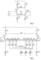
- Fig. 1 contains a first transistor Q11 and a second transistor Q12, which are connected as a differential amplifier.
- the collectors of these transistors are connected via a first resistor R11 or second resistor R12 to the supply voltage U.
- the emitters of these transistors are connected to ground via a first current source IO11 or a second current source IO12.
- the input voltage V in is supplied to the bases of the two transistors.
- the output voltage V out can be tapped between the collectors of the two transistors.
- a variable resistor R10 is connected, with which the gain of the circuit can be adjusted.
- I3 which replaces the adjustable resistor R10 from Fig. 1.
- the six components can be diodes, the forward direction of which points to the current sources I1-I3.
- the AC resistance of these diodes is equal to V T / I, where V T is the temperature voltage and I is the current flowing through the diode.
- the six components can be FET transistors designed as adjustable resistors.
- Particularly linear resistors of this type can be achieved by combining N-MOS and P-MOS transistors.
- the circuit parts Q21, Q22, R21, R22, IO21 and IO22 correspond to the circuit parts Q11, Q12, R11, R12, IO11 and IO12 from Fig. 1st
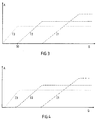
- the number of the circuit parts replacing the resistor R 1 or the number of the divider stages connected in series can be varied in accordance with the requirements for the scope of control, taking into account the available operating voltage level. If the input voltage V in increases starting at a low level, the current in the current source I1 is first reduced.
- the component (the diode) D1a or D1b becomes high-resistance, the influence of any distortions caused by large levels of D1a or D1b on the overall distortions of the amplifier is negligible and the amplification is reduced accordingly.
- the control current of the current source I3 drops at the latest when this control current has become zero. When this control current has become zero, the minimum gain is present. The same applies to any other tax flows.
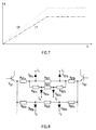
- the output voltage V out may range within the amplifier control independently are held by the level of the input voltage V in constant, whereby the linearity is significantly increased within this control range over the prior art control amplifier.
- the control characteristic of the amplifier in FIG. 2 can be influenced accordingly by the course of the control currents of the current sources I1-I3. A higher control current can also achieve a higher maximum gain.
- the number of control currents can be adapted to the respective requirements of the overall control range and the linearity, however, with an increasing number of control currents or with an increasing amount of control currents, a correspondingly increased operating voltage U is also necessary.
- the amplification factor 30 at the point where the control current of the current source I2 has become zero and the control current of the current source I3 is just starting to decrease, and the corresponding amplification factors for the other control currents, can be determined by reference voltages that correspond to the respective current source I1 , I2 and I3 are supplied.
- Such a dB-linear control characteristic can advantageously be easily achieved with the circuit according to the invention.
- 4 shows a correspondingly improved amplitude profile A of the control currents of the current sources I1, I2 and I3 is plotted against the gain G.
- the individual characteristics have a tanh-like course. The statements relating to FIG. 3 apply accordingly.
- a current source I1, I2, or I3 can be realized which has a characteristic curve corresponding to FIG. 4.
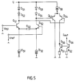
- the common control voltage V AGC and an individual reference voltage V ref are fed to the three current source circuits.
- the control voltage V AGC and the reference voltage V ref arrive at two differential amplifier transistors Q51 and Q52, the emitters of which are connected to ground with a resistor R50 and each via a current source IO51 or IO52.
- the collector of Q51 is connected to the operating voltage U via two diodes D51 and D52 and the collector of Q52 is connected via two diodes D réelle3 and D54.
- the voltage difference between the two collectors is given to the base connections of a further differential amplifier transistor pair Q53 and Q54 and thus controlled depending on the differential amplifier with the transistors Q51 and Q52.
- the emitters of Q53 and Q54 are connected to the operating voltage via a third current source I50.
- the collector of Q53 is grounded.
- the collector of Q54 is connected to the base and collector of a fifth transistor Q55, the emitter of which is connected to ground via a second resistor R51 and the base of which is connected to the base a sixth transistor Q56 is connected.
- the emitter of the sixth transistor is connected to ground via a third resistor R52.
- the respective control current of the current source I1, I2 or I3 can be tapped at the collector.
- the respective steepness of the control current characteristics is given by R50 and the ratio IO50 / I0 and the respective maximum value of the control current by IO50.
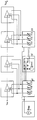
- the IF amplifier block in FIG. 6 contains four individual amplifiers V1-V4, each of which corresponds to a controllable amplifier according to FIG. 2.
- the control currents required by these control amplifiers provide six current source circuits according to FIG. 5, of which the first three are combined to form a first current source block 61 and the other three are combined to form a second current source block 62.
- the first current source block 61 controls the first V1 and second V2 individual amplifiers and the second current source block 63 controls the third V3 and fourth V4 individual amplifiers.
- the number of power source blocks can be between one and four depending on the required control quality.
- a current source block corresponds in each case to three current source circuits according to FIG. 5.
- the current source blocks receive the common control voltage V AGC , but individual reference voltages from the reference voltage block 62.
- the series-connected control amplifiers can advantageously form the essential part of an integrated IF amplifier circuit.
Landscapes
- Engineering & Computer Science (AREA)
- Power Engineering (AREA)
- Amplifiers (AREA)
- Control Of Amplification And Gain Control (AREA)
- Networks Using Active Elements (AREA)
- Microwave Amplifiers (AREA)
Applications Claiming Priority (2)
| Application Number | Priority Date | Filing Date | Title |
|---|---|---|---|
| DE4113498 | 1991-04-25 | ||
| DE4113498A DE4113498C1 (OSRAM) | 1991-04-25 | 1991-04-25 |
Publications (1)
| Publication Number | Publication Date |
|---|---|
| EP0510704A1 true EP0510704A1 (de) | 1992-10-28 |
Family
ID=6430329
Family Applications (2)
| Application Number | Title | Priority Date | Filing Date |
|---|---|---|---|
| EP92909402A Expired - Lifetime EP0581835B3 (de) | 1991-04-25 | 1992-04-25 | Schaltung für einen regelbaren verstärker |
| EP92107119A Pending EP0510704A1 (de) | 1991-04-25 | 1992-04-25 | Schaltung für einen regelbaren Verstärker |
Family Applications Before (1)
| Application Number | Title | Priority Date | Filing Date |
|---|---|---|---|
| EP92909402A Expired - Lifetime EP0581835B3 (de) | 1991-04-25 | 1992-04-25 | Schaltung für einen regelbaren verstärker |
Country Status (13)
| Country | Link |
|---|---|
| US (1) | US5389893A (OSRAM) |
| EP (2) | EP0581835B3 (OSRAM) |
| CN (1) | CN1028395C (OSRAM) |
| AT (1) | ATE170027T1 (OSRAM) |
| DE (2) | DE4113498C1 (OSRAM) |
| ES (1) | ES2121853T7 (OSRAM) |
| HU (1) | HU218637B (OSRAM) |
| MX (1) | MX9201939A (OSRAM) |
| MY (1) | MY110046A (OSRAM) |
| SG (1) | SG46721A1 (OSRAM) |
| TR (1) | TR25846A (OSRAM) |
| WO (1) | WO1992020148A1 (OSRAM) |
| ZA (1) | ZA922984B (OSRAM) |
Cited By (5)
| Publication number | Priority date | Publication date | Assignee | Title |
|---|---|---|---|---|
| DE4329896A1 (de) * | 1993-09-04 | 1995-03-09 | Thomson Brandt Gmbh | Verstärkerstufe mit einer dB-linearen Ausgangsspannung |
| WO1996027239A1 (en) * | 1995-03-01 | 1996-09-06 | Lattice Semiconductor Corporation | Cmos programmable resistor-based transconductor |
| WO1996031946A3 (en) * | 1995-04-05 | 1996-12-27 | Nokia Telecommunications Oy | A linearizer for linearizing a non-linear component controlled by control voltage |
| US5617064A (en) * | 1995-03-01 | 1997-04-01 | Lattice Semiconductor Corporation | Active resistor for stability compensation |
| US5666087A (en) * | 1995-03-01 | 1997-09-09 | Lattice Semiconductor Corp. | Active resistor for stability compensation |
Families Citing this family (13)
| Publication number | Priority date | Publication date | Assignee | Title |
|---|---|---|---|---|
| KR19990044005A (ko) * | 1996-06-21 | 1999-06-25 | 요트.게.아.롤페즈 | 의사 로그 이득 제어의 가변 이득 증폭기 |
| FI106413B (fi) * | 1996-07-11 | 2001-01-31 | Nokia Mobile Phones Ltd | Lineaarisen tehovahvistimen tehonsäätöpiiri |
| FR2765750A1 (fr) * | 1997-07-02 | 1999-01-08 | Trt Lucent Technologies | Dispositif de reception pour signaux hyperfrequence |
| US6084472A (en) * | 1997-12-15 | 2000-07-04 | Analog Devices, Inc. | Multi-tanh triplet with optimal biasing |
| US6084471A (en) * | 1997-12-19 | 2000-07-04 | Nokia Mobile Phones | Soft-limiting control circuit for variable gain amplifiers |
| US6316997B1 (en) * | 2000-03-23 | 2001-11-13 | International Business Machines Corporation | CMOS amplifiers with multiple gain setting control |
| US6333672B1 (en) * | 2000-10-02 | 2001-12-25 | Semiconductor Components Industries Llc | Differential logic circuit and method of use |
| EP1614218B1 (en) * | 2003-04-04 | 2006-07-26 | Koninklijke Philips Electronics N.V. | Linear amplifier |
| US7265623B2 (en) * | 2004-08-03 | 2007-09-04 | Scintera Networks, Inc. | Differential amplifier having independently tunable base gain, peak gain and boost frequency, and uses of same |
| RU2331964C1 (ru) * | 2007-05-21 | 2008-08-20 | ГОУ ВПО "Южно-Российский государственный университет экономики и сервиса" (ЮРГУЭС) | Преобразователь "напряжение-ток" |
| RU2383100C1 (ru) * | 2009-02-10 | 2010-02-27 | Государственное образовательное учреждение высшего профессионального образования "Южно-Российский государственный университет экономики и сервиса" (ГОУ ВПО "ЮРГУЭС") | Радиационно стойкий преобразователь "напряжение - ток" |
| CN104617899A (zh) * | 2015-03-06 | 2015-05-13 | 上海新微技术研发中心有限公司 | 差分放大器和电子设备 |
| RU2658818C1 (ru) * | 2017-05-05 | 2018-06-22 | федеральное государственное бюджетное образовательное учреждение высшего образования "Донской государственный технический университет" (ДГТУ) | Дифференциальный преобразователь "напряжение-ток" с широким диапазоном линейной работы |
Citations (2)
| Publication number | Priority date | Publication date | Assignee | Title |
|---|---|---|---|---|
| US4429416A (en) * | 1982-03-26 | 1984-01-31 | National Semiconductor Corporation | Multistage cascade/cascode limiting IF amplifier and meter circuit |
| DE3522416A1 (de) * | 1985-06-22 | 1987-01-02 | Standard Elektrik Lorenz Ag | Regelbare breitbandverstaerkerschaltung |
Family Cites Families (5)
| Publication number | Priority date | Publication date | Assignee | Title |
|---|---|---|---|---|
| GB2135847A (en) * | 1983-02-14 | 1984-09-05 | Philips Electronic Associated | Amplifier arrangement |
| US4833422A (en) * | 1987-09-24 | 1989-05-23 | Burr-Brown Corporation | Programmable gain instrumentation amplifier |
| US4835488A (en) * | 1988-01-13 | 1989-05-30 | Tektronix, Inc. | Wideband linearized emitter feedback amplifier |
| USH965H (en) * | 1990-01-26 | 1991-09-03 | American Telephone And Telegraph Company | Differential amplifier with digitally controlled gain |
| US5313172A (en) * | 1992-12-11 | 1994-05-17 | Rockwell International Corporation | Digitally switched gain amplifier for digitally controlled automatic gain control amplifier applications |
-
1991
- 1991-04-25 DE DE4113498A patent/DE4113498C1/de not_active Expired - Fee Related
-
1992
- 1992-04-24 ZA ZA922984A patent/ZA922984B/xx unknown
- 1992-04-25 EP EP92909402A patent/EP0581835B3/de not_active Expired - Lifetime
- 1992-04-25 HU HU9302723A patent/HU218637B/hu unknown
- 1992-04-25 ES ES92909402T patent/ES2121853T7/es active Active
- 1992-04-25 SG SG1996009323A patent/SG46721A1/en unknown
- 1992-04-25 AT AT92909402T patent/ATE170027T1/de not_active IP Right Cessation
- 1992-04-25 CN CN92103690A patent/CN1028395C/zh not_active Expired - Lifetime
- 1992-04-25 EP EP92107119A patent/EP0510704A1/de active Pending
- 1992-04-25 WO PCT/EP1992/000912 patent/WO1992020148A1/de not_active Ceased
- 1992-04-25 DE DE59209467T patent/DE59209467D1/de not_active Expired - Lifetime
- 1992-04-27 MX MX9201939A patent/MX9201939A/es unknown
- 1992-04-27 TR TR92/0410A patent/TR25846A/xx unknown
- 1992-05-06 MY MYPI92000781A patent/MY110046A/en unknown
-
1993
- 1993-10-19 US US08/138,852 patent/US5389893A/en not_active Expired - Lifetime
Patent Citations (2)
| Publication number | Priority date | Publication date | Assignee | Title |
|---|---|---|---|---|
| US4429416A (en) * | 1982-03-26 | 1984-01-31 | National Semiconductor Corporation | Multistage cascade/cascode limiting IF amplifier and meter circuit |
| DE3522416A1 (de) * | 1985-06-22 | 1987-01-02 | Standard Elektrik Lorenz Ag | Regelbare breitbandverstaerkerschaltung |
Cited By (7)
| Publication number | Priority date | Publication date | Assignee | Title |
|---|---|---|---|---|
| DE4329896A1 (de) * | 1993-09-04 | 1995-03-09 | Thomson Brandt Gmbh | Verstärkerstufe mit einer dB-linearen Ausgangsspannung |
| WO1996027239A1 (en) * | 1995-03-01 | 1996-09-06 | Lattice Semiconductor Corporation | Cmos programmable resistor-based transconductor |
| US5617064A (en) * | 1995-03-01 | 1997-04-01 | Lattice Semiconductor Corporation | Active resistor for stability compensation |
| US5666087A (en) * | 1995-03-01 | 1997-09-09 | Lattice Semiconductor Corp. | Active resistor for stability compensation |
| WO1996031946A3 (en) * | 1995-04-05 | 1996-12-27 | Nokia Telecommunications Oy | A linearizer for linearizing a non-linear component controlled by control voltage |
| US5847604A (en) * | 1995-04-05 | 1998-12-08 | Nokia Telecommunications Oy | Linearizer for linearizing a non-linear component controlled by control voltage |
| CN1078978C (zh) * | 1995-04-05 | 2002-02-06 | 诺基亚电信公司 | 用于对由控制电压控制的非线性组件线性化的线性化电路 |
Also Published As
| Publication number | Publication date |
|---|---|
| US5389893A (en) | 1995-02-14 |
| EP0581835B3 (de) | 2008-12-03 |
| CN1067535A (zh) | 1992-12-30 |
| EP0581835B1 (de) | 1998-08-19 |
| ES2121853T7 (es) | 2009-06-18 |
| MX9201939A (es) | 1992-11-01 |
| MY110046A (en) | 1997-12-31 |
| ES2121853T3 (es) | 1998-12-16 |
| TR25846A (tr) | 1993-09-01 |
| ZA922984B (en) | 1993-01-27 |
| HU218637B (hu) | 2000-10-28 |
| WO1992020148A1 (de) | 1992-11-12 |
| SG46721A1 (en) | 1998-02-20 |
| ATE170027T1 (de) | 1998-09-15 |
| DE4113498C1 (OSRAM) | 1992-04-30 |
| HUT66223A (en) | 1994-10-28 |
| CN1028395C (zh) | 1995-05-10 |
| DE59209467D1 (de) | 1998-09-24 |
| HU9302723D0 (en) | 1993-12-28 |
| EP0581835A1 (de) | 1994-02-09 |
Similar Documents
| Publication | Publication Date | Title |
|---|---|---|
| EP0581835B1 (de) | Schaltung für einen regelbaren verstärker | |
| DE68927535T2 (de) | Verstärker | |
| DE3044956A1 (de) | "digitaler hochleistungsverstaerker" | |
| DE69020748T2 (de) | Differenzverstärker mit Spannungsverschiebung zur Erzielung einer Eingangsfähigkeit über den ganzen, sehr niedrigen Versorgungsspannungsbereich. | |
| DE3432510C2 (OSRAM) | ||
| DE1904334A1 (de) | Differentialverstaerker fuer vorzugsweise automatische Verstaerkungsregelung | |
| DE3225405C2 (de) | Spannungs/Strom-Wandlerschaltung | |
| DE3036764C2 (OSRAM) | ||
| DE2363624A1 (de) | Schaltungsanordnung zur subtraktion eines vielfachen eines ersten eingangsstromes von einem zweiten eingangsstrom | |
| DE3522416A1 (de) | Regelbare breitbandverstaerkerschaltung | |
| DE3545392C2 (OSRAM) | ||
| DE2924171C2 (OSRAM) | ||
| DE3615383A1 (de) | Eine schaltung zur verschiebung des eingangspegels eines digital-analog-wandlers | |
| DE69320776T2 (de) | Transkonduktanzverstärker | |
| DE69112104T2 (de) | Verstärkerschaltung. | |
| EP0541164B1 (de) | Verstärker | |
| DE1909032C3 (de) | Analog-Digitalwandler | |
| EP0237086A1 (de) | Stromspiegelschaltung | |
| EP0429717B1 (de) | Transkonduktanzverstärker | |
| DE2018923A1 (de) | Schnelle Stromschaltverstärker (Ablenkvers tSrker) | |
| DE19900558A1 (de) | Verstärker für einen Analog-Digital-Wandler | |
| DE2706574C2 (de) | Spannungsgesteuerte Verstärkerschaltung | |
| DE4039983C2 (de) | Steuerbarer Verstärker | |
| DE69121293T2 (de) | Kaskodierter Videoverstärker mit gegenphasigen Ausgangssignalen | |
| DE3816140A1 (de) | Videosignalumschalter |
Legal Events
| Date | Code | Title | Description |
|---|---|---|---|
| PUAI | Public reference made under article 153(3) epc to a published international application that has entered the european phase |
Free format text: ORIGINAL CODE: 0009012 |
|
| AK | Designated contracting states |
Kind code of ref document: A1 Designated state(s): PT |
|
| STAA | Information on the status of an ep patent application or granted ep patent |
Free format text: STATUS: PROCEEDINGS CLOSED FOLLOWING CONSOLIDATION WITH EP92909402.7 |
|
| 17P | Request for examination filed |
Effective date: 19930329 |
|
| XX | Miscellaneous (additional remarks) |
Free format text: VERFAHREN ABGESCHLOSSEN INFOLGE VERBINDUNG MIT 929094027/0581835 (EUROPAEISCHE ANMELDENUMMER/VEROEFFENTLICHUNGSNUMMER) DURCH ENTSCHEIDUNG VOM 10.05.96. |