EP0510704A1 - Circuit for a controllable amplifier - Google Patents
Circuit for a controllable amplifier Download PDFInfo
- Publication number
- EP0510704A1 EP0510704A1 EP92107119A EP92107119A EP0510704A1 EP 0510704 A1 EP0510704 A1 EP 0510704A1 EP 92107119 A EP92107119 A EP 92107119A EP 92107119 A EP92107119 A EP 92107119A EP 0510704 A1 EP0510704 A1 EP 0510704A1
- Authority
- EP
- European Patent Office
- Prior art keywords
- current
- circuit according
- resistors
- control
- series
- Prior art date
- Legal status (The legal status is an assumption and is not a legal conclusion. Google has not performed a legal analysis and makes no representation as to the accuracy of the status listed.)
- Pending
Links
Images
Classifications
-
- H—ELECTRICITY
- H03—ELECTRONIC CIRCUITRY
- H03F—AMPLIFIERS
- H03F3/00—Amplifiers with only discharge tubes or only semiconductor devices as amplifying elements
- H03F3/45—Differential amplifiers
- H03F3/45071—Differential amplifiers with semiconductor devices only
- H03F3/45076—Differential amplifiers with semiconductor devices only characterised by the way of implementation of the active amplifying circuit in the differential amplifier
- H03F3/4508—Differential amplifiers with semiconductor devices only characterised by the way of implementation of the active amplifying circuit in the differential amplifier using bipolar transistors as the active amplifying circuit
- H03F3/45098—PI types
-
- H—ELECTRICITY
- H03—ELECTRONIC CIRCUITRY
- H03G—CONTROL OF AMPLIFICATION
- H03G7/00—Volume compression or expansion in amplifiers
- H03G7/06—Volume compression or expansion in amplifiers having semiconductor devices
- H03G7/08—Volume compression or expansion in amplifiers having semiconductor devices incorporating negative feedback
-
- H—ELECTRICITY
- H03—ELECTRONIC CIRCUITRY
- H03F—AMPLIFIERS
- H03F2203/00—Indexing scheme relating to amplifiers with only discharge tubes or only semiconductor devices as amplifying elements covered by H03F3/00
- H03F2203/45—Indexing scheme relating to differential amplifiers
- H03F2203/45048—Calibrating and standardising a dif amp
-
- H—ELECTRICITY
- H03—ELECTRONIC CIRCUITRY
- H03F—AMPLIFIERS
- H03F2203/00—Indexing scheme relating to amplifiers with only discharge tubes or only semiconductor devices as amplifying elements covered by H03F3/00
- H03F2203/45—Indexing scheme relating to differential amplifiers
- H03F2203/45051—Two or more differential amplifiers cascade coupled
-
- H—ELECTRICITY
- H03—ELECTRONIC CIRCUITRY
- H03F—AMPLIFIERS
- H03F2203/00—Indexing scheme relating to amplifiers with only discharge tubes or only semiconductor devices as amplifying elements covered by H03F3/00
- H03F2203/45—Indexing scheme relating to differential amplifiers
- H03F2203/45466—Indexing scheme relating to differential amplifiers the CSC being controlled, e.g. by a signal derived from a non specified place in the dif amp circuit
-
- H—ELECTRICITY
- H03—ELECTRONIC CIRCUITRY
- H03F—AMPLIFIERS
- H03F2203/00—Indexing scheme relating to amplifiers with only discharge tubes or only semiconductor devices as amplifying elements covered by H03F3/00
- H03F2203/45—Indexing scheme relating to differential amplifiers
- H03F2203/45471—Indexing scheme relating to differential amplifiers the CSC comprising one or more extra current sources
-
- H—ELECTRICITY
- H03—ELECTRONIC CIRCUITRY
- H03F—AMPLIFIERS
- H03F2203/00—Indexing scheme relating to amplifiers with only discharge tubes or only semiconductor devices as amplifying elements covered by H03F3/00
- H03F2203/45—Indexing scheme relating to differential amplifiers
- H03F2203/45506—Indexing scheme relating to differential amplifiers the CSC comprising only one switch
Definitions
- the invention relates to a circuit for a controllable amplifier.
- Adjustable amplifiers are known which e.g. can be used to control the amplitude of IF signals. Such an amplifier is included, for example, in the TDA 4443 integrated circuit. However, these known amplifiers are not low-noise or have a limited linearity or the control characteristic is not dB-linear.
- the invention has for its object to provide a circuit for a controllable amplifier with increased linearity and improved noise behavior. This object is achieved by the circuit according to the invention specified in claim 1.
- the circuit according to the invention is provided with a differential amplifier for an input voltage, which contains a first transistor and a second transistor, which are connected by a series circuit of at least three resistors, at least one component branching off between these resistors, each of which has at least one Power source is connected and the current of these current sources is variable depending on the input voltage.
- the current of the current sources is also advantageously dependent on a reference voltage, the respective reference voltage is lowest for the components located in the middle of the series connection and highest for the components lying closest to the ends of the series connection. It is advantageous in the case of linear control that the currents of the current sources are proportional to one another and become smaller from the center to the ends of the series connection.
- the overall negative feedback network is divided into individual networks, each of which is supplied with at least one control current of its own.
- the individual control currents become smaller with increasing input voltage.
- the control currents can e.g. tanh-shaped (tangent hyperbolic) or similar characteristics obtained.
- such an amplifier is relatively low-noise due to its structure and functional principle.
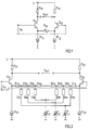
- Fig. 1 contains a first transistor Q11 and a second transistor Q12, which are connected as a differential amplifier.
- the collectors of these transistors are connected via a first resistor R11 or second resistor R12 to the supply voltage U.
- the emitters of these transistors are connected to ground via a first current source IO11 or a second current source IO12.
- the input voltage V in is supplied to the bases of the two transistors.
- the output voltage V out can be tapped between the collectors of the two transistors.
- a variable resistor R10 is connected, with which the gain of the circuit can be adjusted.
- I3 which replaces the adjustable resistor R10 from Fig. 1.
- the six components can be diodes, the forward direction of which points to the current sources I1-I3.
- the AC resistance of these diodes is equal to V T / I, where V T is the temperature voltage and I is the current flowing through the diode.
- the six components can be FET transistors designed as adjustable resistors.
- Particularly linear resistors of this type can be achieved by combining N-MOS and P-MOS transistors.
- the circuit parts Q21, Q22, R21, R22, IO21 and IO22 correspond to the circuit parts Q11, Q12, R11, R12, IO11 and IO12 from Fig. 1st
- the number of the circuit parts replacing the resistor R 1 or the number of the divider stages connected in series can be varied in accordance with the requirements for the scope of control, taking into account the available operating voltage level. If the input voltage V in increases starting at a low level, the current in the current source I1 is first reduced.
- the component (the diode) D1a or D1b becomes high-resistance, the influence of any distortions caused by large levels of D1a or D1b on the overall distortions of the amplifier is negligible and the amplification is reduced accordingly.
- the control current of the current source I3 drops at the latest when this control current has become zero. When this control current has become zero, the minimum gain is present. The same applies to any other tax flows.
- the output voltage V out may range within the amplifier control independently are held by the level of the input voltage V in constant, whereby the linearity is significantly increased within this control range over the prior art control amplifier.
- the control characteristic of the amplifier in FIG. 2 can be influenced accordingly by the course of the control currents of the current sources I1-I3. A higher control current can also achieve a higher maximum gain.
- the number of control currents can be adapted to the respective requirements of the overall control range and the linearity, however, with an increasing number of control currents or with an increasing amount of control currents, a correspondingly increased operating voltage U is also necessary.
- the amplification factor 30 at the point where the control current of the current source I2 has become zero and the control current of the current source I3 is just starting to decrease, and the corresponding amplification factors for the other control currents, can be determined by reference voltages that correspond to the respective current source I1 , I2 and I3 are supplied.
- Such a dB-linear control characteristic can advantageously be easily achieved with the circuit according to the invention.
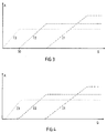
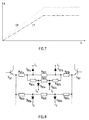
- 4 shows a correspondingly improved amplitude profile A of the control currents of the current sources I1, I2 and I3 is plotted against the gain G.
- the individual characteristics have a tanh-like course. The statements relating to FIG. 3 apply accordingly.
- a current source I1, I2, or I3 can be realized which has a characteristic curve corresponding to FIG. 4.
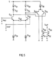
- the common control voltage V AGC and an individual reference voltage V ref are fed to the three current source circuits.
- the control voltage V AGC and the reference voltage V ref arrive at two differential amplifier transistors Q51 and Q52, the emitters of which are connected to ground with a resistor R50 and each via a current source IO51 or IO52.
- the collector of Q51 is connected to the operating voltage U via two diodes D51 and D52 and the collector of Q52 is connected via two diodes D réelle3 and D54.
- the voltage difference between the two collectors is given to the base connections of a further differential amplifier transistor pair Q53 and Q54 and thus controlled depending on the differential amplifier with the transistors Q51 and Q52.
- the emitters of Q53 and Q54 are connected to the operating voltage via a third current source I50.
- the collector of Q53 is grounded.
- the collector of Q54 is connected to the base and collector of a fifth transistor Q55, the emitter of which is connected to ground via a second resistor R51 and the base of which is connected to the base a sixth transistor Q56 is connected.
- the emitter of the sixth transistor is connected to ground via a third resistor R52.
- the respective control current of the current source I1, I2 or I3 can be tapped at the collector.
- the respective steepness of the control current characteristics is given by R50 and the ratio IO50 / I0 and the respective maximum value of the control current by IO50.
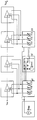
- the IF amplifier block in FIG. 6 contains four individual amplifiers V1-V4, each of which corresponds to a controllable amplifier according to FIG. 2.
- the control currents required by these control amplifiers provide six current source circuits according to FIG. 5, of which the first three are combined to form a first current source block 61 and the other three are combined to form a second current source block 62.
- the first current source block 61 controls the first V1 and second V2 individual amplifiers and the second current source block 63 controls the third V3 and fourth V4 individual amplifiers.
- the number of power source blocks can be between one and four depending on the required control quality.
- a current source block corresponds in each case to three current source circuits according to FIG. 5.
- the current source blocks receive the common control voltage V AGC , but individual reference voltages from the reference voltage block 62.
- the series-connected control amplifiers can advantageously form the essential part of an integrated IF amplifier circuit.
Landscapes
- Engineering & Computer Science (AREA)
- Power Engineering (AREA)
- Amplifiers (AREA)
- Control Of Amplification And Gain Control (AREA)
- Networks Using Active Elements (AREA)
- Microwave Amplifiers (AREA)
Abstract
Description
Die Erfindung betrifft eine Schaltung für einen regelbaren Verstärker.The invention relates to a circuit for a controllable amplifier.
Es sind regelbare Verstärker bekannt, die z.B. zur Amplitudenregelung von ZF-Signalen verwendet werden. Ein solcher Verstärker ist beispielsweise in dem integrierten Schaltkreis vom Typ TDA 4443 enthalten. Diese bekannten Verstärker sind aber nicht rauscharm oder haben eine eingeschränkte Linearität oder die Regelcharakteristik ist nicht dB-linear.Adjustable amplifiers are known which e.g. can be used to control the amplitude of IF signals. Such an amplifier is included, for example, in the TDA 4443 integrated circuit. However, these known amplifiers are not low-noise or have a limited linearity or the control characteristic is not dB-linear.
Der Erfindung liegt die Aufgabe zugrunde, eine Schaltung für einen regelbaren Verstärker mit erhöhter Linearität und verbessertem Rauschverhalten anzugeben. Diese Aufgabe wird durch die in Anspruch 1 angegebene erfindungsgemäße Schaltung gelöst.The invention has for its object to provide a circuit for a controllable amplifier with increased linearity and improved noise behavior. This object is achieved by the circuit according to the invention specified in
Im Prinzip ist die erfindungsgemäße Schaltung versehen mit einem Differenzverstärker für eine Eingangsspannung, der einen ersten Transistor und einen zweiten Transistor enthält, die durch eine Serienschaltung von mindestens drei Widerständen verbunden sind, wobei zwischen diesen Widerständen jeweils mindestens ein Bauelement abzweigt, welches jeweils mit mindestens einer Stromquelle verbunden ist und wobei der Strom dieser Stromquellen in Abhängigkeit von der Eingangsspannung veränderbar ist.
Vorteilhaft ist dabei insbesondere bei einer dB-linearen Regelung der Strom der Stromquellen zusätzlich von einer Referenzspannung abhängig, wobei die jeweilige Referenzspannung für die in der Mitte der Serienschaltung liegenden Bauelemente am niedrigsten und für die am nächsten zu den Enden der Serienschaltung liegenden Bauelemente am höchsten ist. Vorteilhaft bei einer linearen Regelung ist, daß die Ströme der Stromquellen proportional zueinander sind und von der Mitte zu den Enden der Serienschaltung hin kleiner werden.In principle, the circuit according to the invention is provided with a differential amplifier for an input voltage, which contains a first transistor and a second transistor, which are connected by a series circuit of at least three resistors, at least one component branching off between these resistors, each of which has at least one Power source is connected and the current of these current sources is variable depending on the input voltage.
In this case, in particular in the case of a dB-linear control, the current of the current sources is also advantageously dependent on a reference voltage, the respective reference voltage is lowest for the components located in the middle of the series connection and highest for the components lying closest to the ends of the series connection. It is advantageous in the case of linear control that the currents of the current sources are proportional to one another and become smaller from the center to the ends of the series connection.
Vorteilhafte Weiterbildungen der erfindungsgemäßen Schaltung ergeben sich aus den entsprechenden Unteransprüchen.Advantageous developments of the circuit according to the invention result from the corresponding subclaims.
In einem Differenzverstärker wird das Gesamt-Gegenkopplungs-Netzwerk aufgeteilt in einzelne Netzwerke, die jeweils mit mindestens einem eigenen Steuerstrom versorgt werden. Um Verzerrungen durch in den Netzwerken enthaltene nichtlineare Bauelemente, z.B. Diodenstrecken, gering zu halten bzw. die Intermodulationsfestigkeit zu erhöhen, werden die einzelnen Steuerströme mit ansteigender Eingangsspannung kleiner. Zur Realisierung einer dB-linearen Regelcharakteristik können die Steuerströme z.B. tanh-förmige (tangens hyperbolicus) oder ähnliche Kennlinien erhalten. Außerdem ist ein solcher Verstärker aufgrund seiner Struktur und seines Funktionsprinzips relativ rauscharm.In a differential amplifier, the overall negative feedback network is divided into individual networks, each of which is supplied with at least one control current of its own. To avoid distortions caused by non-linear components contained in the networks, e.g. To keep diode paths low or to increase the intermodulation resistance, the individual control currents become smaller with increasing input voltage. To implement a dB-linear control characteristic, the control currents can e.g. tanh-shaped (tangent hyperbolic) or similar characteristics obtained. In addition, such an amplifier is relatively low-noise due to its structure and functional principle.
Anhand der Zeichnungen werden Ausführungsbeispiele der Erfindung beschrieben. Die Zeichnungen zeigen in:
- Fig. 1
- bekannte Schaltung für einen regelbaren Verstärker;
- Fig. 2
- erfindungsgemäße Schaltung für einen regelbaren Verstärker;
- Fig. 3
- Steuerstrom-Kennlinien für den Verstärker nach Fig. 2;
- Fig. 4
- Steuerstrom-Kennlinien für eine dB-lineare Regelcharakteristik;
- Fig. 5
- Schaltung zur Erzeugung von Kennlinien nach Fig. 4;
- Fig. 6
- Verstärker-Block aus mehreren Einzelverstärkern;
- Fig. 7
- Steuerstrom-Kennlinien für eine lineare Regelcharakteristik;
- Fig. 8
- eine weitere erfindungsgemäße Schaltung für ei nen regelbaren Verstärker.
- Fig. 1
- known circuit for a controllable amplifier;
- Fig. 2
- circuit according to the invention for a controllable amplifier;
- Fig. 3
- Control current characteristics for the amplifier of Fig. 2;
- Fig. 4
- Control current characteristics for a dB linear control characteristic;
- Fig. 5
- Circuit for generating characteristic curves according to Fig. 4;
- Fig. 6
- Amplifier block consisting of several individual amplifiers;
- Fig. 7
- Control current characteristics for a linear control characteristic;
- Fig. 8
- another circuit according to the invention for egg NEN controllable amplifier.
Fig. 1 enthält einen ersten Transistor Q₁₁ und einen zweiten Transistor Q₁₂, die als Differenzverstärker geschaltet sind. Die Kollektoren dieser Transistoren sind über einen ersten Widerstand R₁₁ bzw. zweiten Widerstand R₁₂ an die Versorgungsspannung U angeschlossen. Die Emitter dieser Transistoren sind über eine erste Stromquelle IO₁₁ bzw. zweite Stromquelle IO₁₂ an Masse angeschlossen. Den Basen der beiden Transistoren wird die Eingangsspannung Vin zugeführt. Zwischen den Kollektoren der beiden Transistoren ist die Ausgangsspannung Vout abgreifbar. Zwischen den Emittern der beiden Transistoren ist ein regelbarer Widerstand R₁₀ angeschlossen, mit dem die Verstärkung der Schaltung eingestellt werden kann. Für R₁₁ = R₁₂ = R und IO₁₁ = IO₁₂ = IO gilt:
![]()
Fig. 2 enthält ein Netzwerk aus acht in Reihe geschalteten Widerständen R1a-R4a und R1b-R4b, aus sechs jeweils zwischen diesen Widerständen abgehenden Bauelementen D1a-D3a und D1b-D3b und aus drei einseitig an Masse liegenden und an diese Bauelemente angeschlossenen Stromquellen I1-I3, das den regelbaren Widerstand R₁₀ aus Fig. 1 ersetzt.
Im Fall einer Bipolar-Schaltung können die sechs Bauelemente Dioden sein, deren Durchlaßrichtung zu den Stromquellen I1-I3 zeigt. Der Wechselstromwiderstand dieser Dioden ist dabei gleich VT/I, wobei VT die Temperaturspannung und I der durch die Diode fließende Strom ist.Fig. 1 contains a first transistor Q₁₁ and a second transistor Q₁₂, which are connected as a differential amplifier. The collectors of these transistors are connected via a first resistor R₁₁ or second resistor R₁₂ to the supply voltage U. The emitters of these transistors are connected to ground via a first current source IO₁₁ or a second current source IO₁₂. The input voltage V in is supplied to the bases of the two transistors. The output voltage V out can be tapped between the collectors of the two transistors. Between the emitters of the two transistors, a variable resistor R₁₀ is connected, with which the gain of the circuit can be adjusted. For R₁₁ = R₁₂ = R and IO₁₁ = IO₁₂ = IO the following applies:
![]()
2 contains a network of eight resistors R1a-R4a and R1b-R4b connected in series, of six components D1a-D3a and D1b-D3b each going out between these resistors and of three current sources I1- connected to ground on one side and connected to these components. I3, which replaces the adjustable resistor R₁₀ from Fig. 1.
In the case of a bipolar circuit, the six components can be diodes, the forward direction of which points to the current sources I1-I3. The AC resistance of these diodes is equal to V T / I, where V T is the temperature voltage and I is the current flowing through the diode.
Im Fall einer MOS-Schaltung können die sechs Bauelemente als einstellbare Widerstände ausgebildete FET-Transistoren sein. Besonders lineare Widerstände dieser Art lassen sich durch die Kombination von N-MOS- und P-MOS-Transistoren erreichen.In the case of a MOS circuit, the six components can be FET transistors designed as adjustable resistors. Particularly linear resistors of this type can be achieved by combining N-MOS and P-MOS transistors.
Die Schaltungsteile Q₂₁, Q₂₂, R₂₁, R₂₂, IO₂₁ und IO₂₂ entsprechen den Schaltungsteilen Q₁₁, Q₁₂, R₁₁, R₁₂, IO₁₁ und IO₁₂ aus Fig. 1.
Die Anzahl der den Widerstand R₁₀ ersetzenden Schaltungsteile bzw. die Anzahl der hintereinandergeschalteten Teilerstufen kann entsprechend den Erfordernissen für den Regelumfang unter Berücksichtigung der zur Verfügung stehenden Betriebsspannungshöhe variiert werden.
Wenn beginnend bei einem kleinen Pegel die Eingangsspannung Vin ansteigt, wird zunächst der Strom in der Stromquelle I1 zurückgenommen. Dadurch wird das Bauelement (die Diode) D1a bzw. D1b hochohmig, der Einfluß eventueller, durch große Pegel an D1a bzw. D1b bedingter Verzerrungen auf die Gesamtverzerrungen des Verstärkers wird vernachlässigbar und die Verstärkung wird entsprechend verringert. Die Bauelemente R1a und R2a bzw. R1b und R2b wirken nun für das Bauelement D2a bzw. D2b wie ein Spannungsteiler mit vergrößertem Teilerverhältnis, sodaß für die Eingangsspannung Vin in Bezug auf D2a bzw. D2b größere Pegel zulässig sind. Dieser Vorgang setzt sich für weiter ansteigende Eingangsspannungen für die entsprechenden folgenden Bauelemente fort.
Es kann beispielsweise folgende Dimensionierung vorgenommen werden:
R₂₁ = R₂₂ = 3.9 kΩ
R1a = R1b = 100 Ω
R2a = R2b = 1.38kΩ
R3a = R3b = 1.26kΩ
R4a = R4b = 1.26kΩ
In Fig. 3 ist der Amplitudenverlauf A der Steuerströme der Stromquellen I1, I2 und I3 über der Verstärkung G aufgetragen. Bei großer Verstärkung (d.h. kleiner Eingangsspannung Vin) haben alle Steuerströme ihren Maximalwert. Bei steigender Eingangsspannung (d.h. sinkender Verstärkung) wird zunächst Steuerstrom der Stromquelle 11 zurückgenommen. Spätestens wenn dieser Steuerstrom zu Null geworden ist, fällt der Steuerstrom der Stromquelle I2. Spätestens wenn dieser Steuerstrom zu Null geworden ist, fällt der Steuerstrom der Stromquelle I3. Wenn dieser Steuerstrom zu Null geworden ist, liegt die Minimal-Verstärkung vor. Entsprechendes gilt für eventuelle weitere Steuerströme.
Auf diese Weise kann die Ausgangsspannung Vout innerhalb des Verstärker-Regelbereichs unabhängig vom Pegel der Eingangsspannung Vin konstant gehalten werden, wobei die Linearität innerhalb dieses Regelbereichs gegenüber dem bekannten Regelverstärker deutlich erhöht ist.
Durch den Verlauf der Steuerströme der Stromquellen I1-I3 kann die Regelcharakteristik des Verstärkers in Fig. 2 entsprechend beeinflußt werden. Durch einen höheren Steuerstrom kann auch eine höhere Maximalverstärkung erreicht werden. Die Anzahl der Steuerströme kann den jeweiligen Erfordernissen an den Gesamt-Regelbereich und an die Linearität angepaßt werden, jedoch ist bei steigender Anzahl von Steuerströmen oder bei steigendem Betrag der Steuerströme auch eine entsprechend erhöhte Betriebsspannung U erforderlich. Der Verstärkungs-Faktor 30 an der Stelle, wo der Steuerstrom der Stromquelle I2 zu Null geworden ist und der Steuerstrom der Stromquelle I3 gerade mit der Absenkung beginnt sowie die entsprechenden Verstärkungfaktoren für die anderen Steuerströme, lassen sich durch Referenzspannungen festlegen, die der jeweiligen Stromquelle I1, I2 und I3 zugeführt werden.The circuit parts Q₂₁, Q₂₂, R₂₁, R₂₂, IO₂₁ and IO₂₂ correspond to the circuit parts Q₁₁, Q₁₂, R₁₁, R₁₂, IO₁₁ and IO₁₂ from Fig. 1st
The number of the circuit parts replacing the
If the input voltage V in increases starting at a low level, the current in the current source I1 is first reduced. As a result, the component (the diode) D1a or D1b becomes high-resistance, the influence of any distortions caused by large levels of D1a or D1b on the overall distortions of the amplifier is negligible and the amplification is reduced accordingly. The components 1a and R 2a or R1b and R2b now acting for the component D2a or D2b as a voltage divider with an enlarged divider ratio so that the input voltage Vin with respect to D2a or D2b greater level are permissible. This process continues for further increasing input voltages for the corresponding subsequent components.
The following dimensioning can be carried out, for example:
R₂₁ = R₂₂ = 3.9 kΩ
R1a = R1b = 100 Ω
R2a = R2b = 1.38kΩ
R3a = R3b = 1.26kΩ
R4a = R4b = 1.26kΩ
In Fig. 3, the amplitude curve A of the control currents of the current sources I1, I2 and I3 is plotted against the gain G. With large amplification (ie low input voltage V in ) all control currents have their maximum value. When the input voltage increases (ie the gain drops), the control current of the
In this way, the output voltage V out may range within the amplifier control independently are held by the level of the input voltage V in constant, whereby the linearity is significantly increased within this control range over the prior art control amplifier.
The control characteristic of the amplifier in FIG. 2 can be influenced accordingly by the course of the control currents of the current sources I1-I3. A higher control current can also achieve a higher maximum gain. The number of control currents can be adapted to the respective requirements of the overall control range and the linearity, however, with an increasing number of control currents or with an increasing amount of control currents, a correspondingly increased operating voltage U is also necessary. The
Ein ZF-Verstärker hat z.B. einen Regelumfang von 60dB. Wenn mit einer Kontrollspannung VAGC beispielsweise eine Verstärkung von 6dB eingestellt werden soll, ergibt sich bei einer linearen Regelungscharakteristik diese Kontrollspannung zu nur
VAGC6dB=(2/1000)*VAGCmax (6dB=Faktor 2, 60dB=Faktor 1000).For example, an IF amplifier has a control range of 60dB. If, for example, a control voltage V AGC is to be used to set a gain of 6 dB, this control voltage only results in the case of a linear control characteristic
V AGC6dB = (2/1000) * V AGCmax (6dB = factor 2, 60dB = factor 1000).
Bei einer dB-linearen Regelungscharakteristik ergäbe sich dagegen eine Kontrollspannung von
VAGC6dB= (6/60)*VAGCmax.
Darum hat eine dB-lineare Regelungscharakteristik Vorteile bezüglich der Einfachheit der Regelung, der Regelgeschwindigkeit und der Regelstabilität (Regelsprünge).A dB-linear control characteristic, on the other hand, would result in a control voltage of
V AGC6dB = (6/60) * V AGCmax .
That is why a dB-linear control characteristic has advantages in terms of the simplicity of the control, the control speed and the control stability (control jumps).
Mit der erfindungsgemäßen Schaltung läßt sich vorteilhaft leicht eine solche dB-lineare Regelungscharakteristik erreichen. In Fig. 4 ist ein entsprechend verbesserter Amplitudenverlauf A der Steuerströme der Stromquellen I1, I2 und I3 über der Verstärkung G aufgetragen. Die einzelnen Kennlinien haben einen tanh-ähnlichen Verlauf. Die Aussagen zu Fig. 3 gelten hier entsprechend.Such a dB-linear control characteristic can advantageously be easily achieved with the circuit according to the invention. 4 shows a correspondingly improved amplitude profile A of the control currents of the current sources I1, I2 and I3 is plotted against the gain G. The individual characteristics have a tanh-like course. The statements relating to FIG. 3 apply accordingly.
Mit einer Stromquellen-Schaltung nach Fig. 5 läßt sich eine Stromquelle I1, I2, oder I3 realisieren, die eine der Fig. 4 entsprechende Kennlinie hat.
Den drei Stromquellen-Schaltungen wird die gemeinsame Kontrollspannung VAGC und jeweils eine individuelle Referenzspannung Vref zugeführt. Die Kontrollspannung VAGC und die Referenzspannung Vref gelangen zu zwei Differenzverstärker-Transistoren Q₅₁ bzw. Q₅₂, deren Emitter mit einem Widerstand R₅₀ untereinander und jeweils über eine Stromquelle IO₅₁ bzw. IO₅₂ mit Masse verbunden sind. Der Kollektor von Q₅₁ ist über zwei Dioden D₅₁ und D₅₂ und der Kollektor von Q₅₂ ist über zwei Dioden D₅₃ und D₅₄ mit der Betriebsspannung U verbunden. Die Spannungsdifferenz zwischen den beiden Kollektoren wird auf die Basisanschlüsse eines weiteren Differenzverstärker-Transistorenpaars Q₅₃ und Q₅₄ gegeben und somit in Abhängigkeit vom Differenzverstärker mit den Transistoren Q₅₁ und Q₅₂ gesteuert. Die Emitter von Q₅₃ und Q₅₄ sind über eine dritte Stromquelle I₅₀ mit der Betriebsspannung verbunden. Der Kollektor von Q₅₃ liegt an Masse. Der Kollektor von Q₅₄ ist mit Basis und Kollektor eines fünften Transistors Q₅₅ verbunden, dessen Emitter über einen zweiten Widerstand R₅₁ an Masse liegt und dessen Basis an die Basis eines sechsten Transistors Q₅₆ angeschlossen ist. Der Emitter des sechsten Transistors liegt über einen dritten Widerstand R₅₂ an Masse. Am Kollektor ist der jeweilige Steuerstrom der Stromquelle I1, I2 oder I3 abgreifbar.
Es sei v = (VAGC-Vref), I₀ der von den Stromquellen IO₅₁ und IO₅₂ und IO₅₂ der von der Stromquelle I₅₀ eingeprägte Strom. Dann ergibt sich der jeweilige Ausgangsstrom Iout zu
![]()
wobei n der Index der jeweiligen Kennlinie (n = 1,2,3), k die Anzahl der hintereinandergeschalteten Dioden und C eine Konstante ist, z.B. C = 3. In der Stromquellen-Schaltung nach Fig. 5 ist daher k = 2. Die jeweilige Steilheit der Steuerstrom-Kennlinien ist durch R₅₀ und das Verhältnis IO₅₀/I₀ und der jeweilige Maximalwert des Steuerstroms durch IO₅₀ gegeben.
Es kann beispielsweise für den in Fig. 6 beschriebenen ersten Stromquellenblock 61 folgende Dimensionierung vorgenommen werden:
U = 7.7V
Stromquelle I1:
R₅₀ = 8.0kΩ
R₅₁ = R₅₂ = 2.7kΩ
I₀ = 167µA
Strom von I₅₀ = 103µA
Vref = 3.624V
Stromquelle I2:
R₅₀ = 10.0kΩ
R₅₁ = R₅₂ = 2.25kΩ
I₀ = 50.6µA
Strom von I₅₀ = 103µA
Vref = 2.676V
Stromquelle 13:
R₅₀ = 4.0kΩ
R₅₁ = R₅₂ = 1.5kΩ
I₀ = 50.5µA
Strom von I₅₀ = 103µA
Vref = 2.179V
Für den in Fig. 6 beschriebenen zweiten Stromquellenblock 63 ergibt sich folgende abweichende Dimensionierung:
Stromquelle I1:
I₀ = 169µA
Vref = 5.67V
Stromquelle I2:
I₀ = 51.4µA
Vref = 4.766V
Stromquelle I3:
I₀ = 51.3µA
Vref = 4.326V
Der ZF-Verstärker-Block in Fig. 6 enthält vier Einzelverstärker V1-V4, die jeweils einem regelbaren Verstärker nach Fig. 2 entsprechen. Die von diesen Regelverstärkern benötigten Steuerströme liefern sechs Stromquellen-Schaltungen gemäß Fig. 5, von denen die ersten drei zu einem ersten Stromquellen-Block 61 und die anderen drei zu einem zweiten Stromquellen-Block 62 zusammengefaßt sind. Der erste Stromquellen-Block 61 steuert den ersten V1 und zweiten V2 Einzelverstärker und der zweite Stromquellen-Block 63 den dritten V3 und vierten V4 Einzelverstärker. Die Anzahl der Stromquellen-Blöcke kann je nach verlangter Regelqualität zwischen eins und vier liegen.
Ein Stromquellen-Block entspricht jeweils drei Stromquellen-Schaltungen nach Fig. 5. Die Stromquellen-Blöcke erhalten die gemeinsame Kontrollspannung VAGC, aber individuelle Referenzspannungen aus dem Referenzspannungsblock 62.5, a current source I1, I2, or I3 can be realized which has a characteristic curve corresponding to FIG. 4.
The common control voltage V AGC and an individual reference voltage V ref are fed to the three current source circuits. The control voltage V AGC and the reference voltage V ref arrive at two differential amplifier transistors Q₅₁ and Q₅₂, the emitters of which are connected to ground with a resistor R₅₀ and each via a current source IO₅₁ or IO₅₂. The collector of Q₅₁ is connected to the operating voltage U via two diodes D₅₁ and D₅₂ and the collector of Q₅₂ is connected via two diodes D zwei₃ and D₅₄. The voltage difference between the two collectors is given to the base connections of a further differential amplifier transistor pair Q₅₃ and Q₅₄ and thus controlled depending on the differential amplifier with the transistors Q₅₁ and Q₅₂. The emitters of Q₅₃ and Q₅₄ are connected to the operating voltage via a third current source I₅₀. The collector of Q₅₃ is grounded. The collector of Q₅₄ is connected to the base and collector of a fifth transistor Q₅₅, the emitter of which is connected to ground via a second resistor R₅₁ and the base of which is connected to the base a sixth transistor Q₅₆ is connected. The emitter of the sixth transistor is connected to ground via a third resistor R₅₂. The respective control current of the current source I1, I2 or I3 can be tapped at the collector.
Let v = (V AGC -V ref ), I₀ the current sources IO₅₁ and IO₅₂ and IO₅₂ the current impressed by the current source I₅₀. Then the respective output current I out results
![]()
where n is the index of the respective characteristic curve (n = 1, 2, 3), k is the number of diodes connected in series and C is a constant, for example C = 3. In the current source circuit according to FIG. 5, k is therefore 2. The The respective steepness of the control current characteristics is given by R₅₀ and the ratio IO₅₀ / I₀ and the respective maximum value of the control current by IO₅₀.
For example, the following dimensioning can be carried out for the first
U = 7.7V
Current source I1:
R₅₀ = 8.0kΩ
R₅₁ = R₅₂ = 2.7kΩ
I₀ = 167µA
Current of I₅₀ = 103µA
V ref = 3,624V
Current source I2:
R₅₀ = 10.0kΩ
R₅₁ = R₅₂ = 2.25kΩ
I₀ = 50.6µA
Current of I₅₀ = 103µA
V ref = 2,676V
Power source 13:
R₅₀ = 4.0kΩ
R₅₁ = R₅₂ = 1.5kΩ
I₀ = 50.5µA
Current of I₅₀ = 103µA
V ref = 2,179V
The following different dimensioning results for the second
Current source I1:
I₀ = 169µA
V ref = 5.67V
Current source I2:
I₀ = 51.4µA
V ref = 4.766V
Current source I3:
I₀ = 51.3µA
V ref = 4,326V
The IF amplifier block in FIG. 6 contains four individual amplifiers V1-V4, each of which corresponds to a controllable amplifier according to FIG. 2. The control currents required by these control amplifiers provide six current source circuits according to FIG. 5, of which the first three are combined to form a first
A current source block corresponds in each case to three current source circuits according to FIG. 5. The current source blocks receive the common control voltage V AGC , but individual reference voltages from the
Vorteilhaft können die hintereinandergeschalteten Regelverstärker den wesentlichen Anteil eines integrierten ZF-Verstärker-Schaltkreises bilden.The series-connected control amplifiers can advantageously form the essential part of an integrated IF amplifier circuit.
Bei einer Ansteuerung mit nur zwei Steuerströmen entsprechend Fig. 7 kann man eine lineare Regelcharakteristik erhalten. Dazu kann in Fig. 2 beispielsweise folgende Dimensionierung vorgenommen werden:
R₂₁ = R₂₂ = 3.0 kΩ
R1a = R1b = 100 Ω
R3a = R3b = 2.486kΩ
R4a = R4b = 158 Ω
R2a, R2b und I2 entfallen.With a control with only two control currents according to FIG. 7, a linear control characteristic can be obtained. For this purpose, the following dimensioning can be carried out in FIG. 2:
R₂₁ = R₂₂ = 3.0 kΩ
R1a = R1b = 100 Ω
R3a = R3b = 2,486kΩ
R4a = R4b = 158 Ω
R2a, R2b and I2 are omitted.
Anstelle des Netzwerks aus den acht in Reihe geschalteten Widerständen R1a-R4a und R1b-R4b, aus sechs jeweils zwischen diesen Widerständen abgehenden Bauelementen D1a-D3a und D1b-D3b und aus drei einseitig an Masse liegenden und an diese Bauelemente angeschlossenen Stromquellen I1-I3 in Fig. 2 kann auch das in Fig. 8 dargestellte Netzwerk verwendet werden.
Es sind jeweils in Serie zwischen den Emittern der den Transistoren Q₂₁ und Q₂₂ entsprechenden Transistoren Q₈₁ und Q₈₂ angeordnet:
- die Widerstände R81a, R₈₀₁, R81b mit den zwischen ihnen abzweigenden Dioden D81a und D81b, die an Stromquellen I1 angeschlossen sind;
- die Widerstände R83a, R₈₀₃, R83b mit den zwischen ihnen abzweigenden Dioden D83a und D83b, die an Stromquellen I3 angeschlossen sind;
- die Widerstände R82a, R₈₀₂, R82b mit den zwischen ihnen abzweigenden Dioden D82a und D82b, die an Stromquellen I2 angeschlossen sind, wobei die Widerstände R82a und R82b statt an die Emitter der beiden Transistoren an die Widerstände R81a-R₈₀₁ bzw. R81b-R₈₀₁ angeschlossen sind.
Parallel zu R₈₀₂ können weitere entsprechende Bauelemente und Stromquellen angeschlossen sein.
There are in each case arranged in series between the emitters of the transistors Q₈₁ and Q₈₂ corresponding to the transistors Q₂₁ and Q₂₂:
- the resistors R 81a , R₈₀₁, R 81b with the diodes D 81a and D 81b branching between them, which are connected to current sources I1;
- the resistors R 83a , R₈₀₃, R 83b with the diodes D 83a and D 83b branching between them, which are connected to current sources I3;
- the resistors R 82a , R₈₀₂, R 82b with the diodes D 82a and D 82b branching between them, which are connected to current sources I2, the resistors R 82a and R 82b being instead of the emitters of the two transistors on the resistors R 81a -R₈₀₁ or R 81b -R₈₀₁ are connected.
In parallel to R₈₀₂ further corresponding components and power sources can be connected.
Claims (11)
Applications Claiming Priority (2)
| Application Number | Priority Date | Filing Date | Title |
|---|---|---|---|
| DE4113498 | 1991-04-25 | ||
| DE4113498A DE4113498C1 (en) | 1991-04-25 | 1991-04-25 |
Publications (1)
| Publication Number | Publication Date |
|---|---|
| EP0510704A1 true EP0510704A1 (en) | 1992-10-28 |
Family
ID=6430329
Family Applications (2)
| Application Number | Title | Priority Date | Filing Date |
|---|---|---|---|
| EP92107119A Pending EP0510704A1 (en) | 1991-04-25 | 1992-04-25 | Circuit for a controllable amplifier |
| EP92909402A Expired - Lifetime EP0581835B3 (en) | 1991-04-25 | 1992-04-25 | Circuit for controllable amplifier |
Family Applications After (1)
| Application Number | Title | Priority Date | Filing Date |
|---|---|---|---|
| EP92909402A Expired - Lifetime EP0581835B3 (en) | 1991-04-25 | 1992-04-25 | Circuit for controllable amplifier |
Country Status (13)
| Country | Link |
|---|---|
| US (1) | US5389893A (en) |
| EP (2) | EP0510704A1 (en) |
| CN (1) | CN1028395C (en) |
| AT (1) | ATE170027T1 (en) |
| DE (2) | DE4113498C1 (en) |
| ES (1) | ES2121853T7 (en) |
| HU (1) | HU218637B (en) |
| MX (1) | MX9201939A (en) |
| MY (1) | MY110046A (en) |
| SG (1) | SG46721A1 (en) |
| TR (1) | TR25846A (en) |
| WO (1) | WO1992020148A1 (en) |
| ZA (1) | ZA922984B (en) |
Cited By (5)
| Publication number | Priority date | Publication date | Assignee | Title |
|---|---|---|---|---|
| DE4329896A1 (en) * | 1993-09-04 | 1995-03-09 | Thomson Brandt Gmbh | Amplifier stage with a dB linear output voltage |
| WO1996027239A1 (en) * | 1995-03-01 | 1996-09-06 | Lattice Semiconductor Corporation | Cmos programmable resistor-based transconductor |
| WO1996031946A2 (en) * | 1995-04-05 | 1996-10-10 | Nokia Telecommunications Oy | A linearizer for linearizing a non-linear component controlled by control voltage |
| US5617064A (en) * | 1995-03-01 | 1997-04-01 | Lattice Semiconductor Corporation | Active resistor for stability compensation |
| US5666087A (en) * | 1995-03-01 | 1997-09-09 | Lattice Semiconductor Corp. | Active resistor for stability compensation |
Families Citing this family (10)
| Publication number | Priority date | Publication date | Assignee | Title |
|---|---|---|---|---|
| EP0846369A1 (en) * | 1996-06-21 | 1998-06-10 | Koninklijke Philips Electronics N.V. | Variable-gain amplifier with pseudo-logarithmic gain control |
| FI106413B (en) * | 1996-07-11 | 2001-01-31 | Nokia Mobile Phones Ltd | Linear power amplifier power control circuit |
| FR2765750A1 (en) * | 1997-07-02 | 1999-01-08 | Trt Lucent Technologies | RECEIVING DEVICE FOR MICROWAVE SIGNALS |
| US6084472A (en) * | 1997-12-15 | 2000-07-04 | Analog Devices, Inc. | Multi-tanh triplet with optimal biasing |
| US6084471A (en) * | 1997-12-19 | 2000-07-04 | Nokia Mobile Phones | Soft-limiting control circuit for variable gain amplifiers |
| US6316997B1 (en) * | 2000-03-23 | 2001-11-13 | International Business Machines Corporation | CMOS amplifiers with multiple gain setting control |
| US6333672B1 (en) * | 2000-10-02 | 2001-12-25 | Semiconductor Components Industries Llc | Differential logic circuit and method of use |
| US7265623B2 (en) * | 2004-08-03 | 2007-09-04 | Scintera Networks, Inc. | Differential amplifier having independently tunable base gain, peak gain and boost frequency, and uses of same |
| CN104617899A (en) * | 2015-03-06 | 2015-05-13 | 上海新微技术研发中心有限公司 | differential amplifier and electronic device |
| RU2658818C1 (en) * | 2017-05-05 | 2018-06-22 | федеральное государственное бюджетное образовательное учреждение высшего образования "Донской государственный технический университет" (ДГТУ) | Differential voltage-current converter with wide range of linear operation |
Citations (2)
| Publication number | Priority date | Publication date | Assignee | Title |
|---|---|---|---|---|
| US4429416A (en) * | 1982-03-26 | 1984-01-31 | National Semiconductor Corporation | Multistage cascade/cascode limiting IF amplifier and meter circuit |
| DE3522416A1 (en) * | 1985-06-22 | 1987-01-02 | Standard Elektrik Lorenz Ag | Controllable broadband amplifier circuit |
Family Cites Families (5)
| Publication number | Priority date | Publication date | Assignee | Title |
|---|---|---|---|---|
| GB2135847A (en) * | 1983-02-14 | 1984-09-05 | Philips Electronic Associated | Amplifier arrangement |
| US4833422A (en) * | 1987-09-24 | 1989-05-23 | Burr-Brown Corporation | Programmable gain instrumentation amplifier |
| US4835488A (en) * | 1988-01-13 | 1989-05-30 | Tektronix, Inc. | Wideband linearized emitter feedback amplifier |
| USH965H (en) * | 1990-01-26 | 1991-09-03 | American Telephone And Telegraph Company | Differential amplifier with digitally controlled gain |
| US5313172A (en) * | 1992-12-11 | 1994-05-17 | Rockwell International Corporation | Digitally switched gain amplifier for digitally controlled automatic gain control amplifier applications |
-
1991
- 1991-04-25 DE DE4113498A patent/DE4113498C1/de not_active Expired - Fee Related
-
1992
- 1992-04-24 ZA ZA922984A patent/ZA922984B/en unknown
- 1992-04-25 EP EP92107119A patent/EP0510704A1/en active Pending
- 1992-04-25 HU HU9302723A patent/HU218637B/en unknown
- 1992-04-25 ES ES92909402T patent/ES2121853T7/en active Active
- 1992-04-25 AT AT92909402T patent/ATE170027T1/en not_active IP Right Cessation
- 1992-04-25 EP EP92909402A patent/EP0581835B3/en not_active Expired - Lifetime
- 1992-04-25 DE DE59209467T patent/DE59209467D1/en not_active Expired - Lifetime
- 1992-04-25 WO PCT/EP1992/000912 patent/WO1992020148A1/en active IP Right Grant
- 1992-04-25 SG SG1996009323A patent/SG46721A1/en unknown
- 1992-04-25 CN CN92103690A patent/CN1028395C/en not_active Expired - Lifetime
- 1992-04-27 TR TR92/0410A patent/TR25846A/en unknown
- 1992-04-27 MX MX9201939A patent/MX9201939A/en unknown
- 1992-05-06 MY MYPI92000781A patent/MY110046A/en unknown
-
1993
- 1993-10-19 US US08/138,852 patent/US5389893A/en not_active Expired - Lifetime
Patent Citations (2)
| Publication number | Priority date | Publication date | Assignee | Title |
|---|---|---|---|---|
| US4429416A (en) * | 1982-03-26 | 1984-01-31 | National Semiconductor Corporation | Multistage cascade/cascode limiting IF amplifier and meter circuit |
| DE3522416A1 (en) * | 1985-06-22 | 1987-01-02 | Standard Elektrik Lorenz Ag | Controllable broadband amplifier circuit |
Cited By (8)
| Publication number | Priority date | Publication date | Assignee | Title |
|---|---|---|---|---|
| DE4329896A1 (en) * | 1993-09-04 | 1995-03-09 | Thomson Brandt Gmbh | Amplifier stage with a dB linear output voltage |
| WO1996027239A1 (en) * | 1995-03-01 | 1996-09-06 | Lattice Semiconductor Corporation | Cmos programmable resistor-based transconductor |
| US5617064A (en) * | 1995-03-01 | 1997-04-01 | Lattice Semiconductor Corporation | Active resistor for stability compensation |
| US5666087A (en) * | 1995-03-01 | 1997-09-09 | Lattice Semiconductor Corp. | Active resistor for stability compensation |
| WO1996031946A2 (en) * | 1995-04-05 | 1996-10-10 | Nokia Telecommunications Oy | A linearizer for linearizing a non-linear component controlled by control voltage |
| WO1996031946A3 (en) * | 1995-04-05 | 1996-12-27 | Nokia Telecommunications Oy | A linearizer for linearizing a non-linear component controlled by control voltage |
| US5847604A (en) * | 1995-04-05 | 1998-12-08 | Nokia Telecommunications Oy | Linearizer for linearizing a non-linear component controlled by control voltage |
| CN1078978C (en) * | 1995-04-05 | 2002-02-06 | 诺基亚电信公司 | Alinearizer for linearizing a non-linear component controlled by control voltage |
Also Published As
| Publication number | Publication date |
|---|---|
| US5389893A (en) | 1995-02-14 |
| TR25846A (en) | 1993-09-01 |
| CN1028395C (en) | 1995-05-10 |
| HU218637B (en) | 2000-10-28 |
| ES2121853T3 (en) | 1998-12-16 |
| HUT66223A (en) | 1994-10-28 |
| CN1067535A (en) | 1992-12-30 |
| ZA922984B (en) | 1993-01-27 |
| MX9201939A (en) | 1992-11-01 |
| ATE170027T1 (en) | 1998-09-15 |
| DE4113498C1 (en) | 1992-04-30 |
| WO1992020148A1 (en) | 1992-11-12 |
| MY110046A (en) | 1997-12-31 |
| EP0581835B3 (en) | 2008-12-03 |
| EP0581835B1 (en) | 1998-08-19 |
| DE59209467D1 (en) | 1998-09-24 |
| HU9302723D0 (en) | 1993-12-28 |
| SG46721A1 (en) | 1998-02-20 |
| EP0581835A1 (en) | 1994-02-09 |
| ES2121853T7 (en) | 2009-06-18 |
Similar Documents
| Publication | Publication Date | Title |
|---|---|---|
| EP0581835B1 (en) | Circuit for controllable amplifier | |
| DE68927535T2 (en) | amplifier | |
| DE3044956A1 (en) | "DIGITAL HIGH PERFORMANCE AMPLIFIER" | |
| DE69020748T2 (en) | Differential amplifier with voltage shift to achieve input capability over the entire, very low supply voltage range. | |
| DE3225405C2 (en) | Voltage / current converter circuit | |
| DE3036764C2 (en) | ||
| DE3339498A1 (en) | FAST LOGICAL CIRCUIT | |
| DE3432510C2 (en) | ||
| DE2506318C2 (en) | ||
| DE2363624A1 (en) | CIRCUIT ARRANGEMENT FOR SUBTRACTING A MULTIPLE FIRST INPUT CURRENT FROM A SECOND INPUT CURRENT | |
| DE3522416A1 (en) | Controllable broadband amplifier circuit | |
| DE3545392C2 (en) | ||
| DE2924171C2 (en) | ||
| DE3615383A1 (en) | A CIRCUIT TO SHIFT THE INPUT LEVEL OF A DIGITAL-ANALOG CONVERTER | |
| DE69320776T2 (en) | Transconductance amplifier | |
| DE69112104T2 (en) | Amplifier circuit. | |
| EP0541164B1 (en) | Amplifier | |
| EP0608694B1 (en) | Integratable current source circuit | |
| DE1909032C3 (en) | Analog-to-digital converter | |
| EP0237086A1 (en) | Current mirror circuit | |
| DE3008469C2 (en) | ||
| DE2018923A1 (en) | Fast current switching amplifier (deflection amplifier) | |
| DE2706574C2 (en) | Voltage controlled amplifier circuit | |
| DE4039983C2 (en) | Controllable amplifier | |
| DE69121293T2 (en) | Cascoded video amplifier with antiphase output signals |
Legal Events
| Date | Code | Title | Description |
|---|---|---|---|
| PUAI | Public reference made under article 153(3) epc to a published international application that has entered the european phase |
Free format text: ORIGINAL CODE: 0009012 |
|
| AK | Designated contracting states |
Kind code of ref document: A1 Designated state(s): PT |
|
| STAA | Information on the status of an ep patent application or granted ep patent |
Free format text: STATUS: PROCEEDINGS CLOSED FOLLOWING CONSOLIDATION WITH EP92909402.7 |
|
| 17P | Request for examination filed |
Effective date: 19930329 |
|
| XX | Miscellaneous (additional remarks) |
Free format text: VERFAHREN ABGESCHLOSSEN INFOLGE VERBINDUNG MIT 929094027/0581835 (EUROPAEISCHE ANMELDENUMMER/VEROEFFENTLICHUNGSNUMMER) DURCH ENTSCHEIDUNG VOM 10.05.96. |