EP0509227B1 - Verarbeitungseinrichtung mit Reserveprozessor - Google Patents
Verarbeitungseinrichtung mit Reserveprozessor Download PDFInfo
- Publication number
- EP0509227B1 EP0509227B1 EP19920103999 EP92103999A EP0509227B1 EP 0509227 B1 EP0509227 B1 EP 0509227B1 EP 19920103999 EP19920103999 EP 19920103999 EP 92103999 A EP92103999 A EP 92103999A EP 0509227 B1 EP0509227 B1 EP 0509227B1
- Authority
- EP
- European Patent Office
- Prior art keywords
- task
- cpu
- memory
- data
- flip
- Prior art date
- Legal status (The legal status is an assumption and is not a legal conclusion. Google has not performed a legal analysis and makes no representation as to the accuracy of the status listed.)
- Expired - Lifetime
Links
Images


Classifications
-
- G—PHYSICS
- G06—COMPUTING OR CALCULATING; COUNTING
- G06F—ELECTRIC DIGITAL DATA PROCESSING
- G06F11/00—Error detection; Error correction; Monitoring
- G06F11/07—Responding to the occurrence of a fault, e.g. fault tolerance
- G06F11/16—Error detection or correction of the data by redundancy in hardware
- G06F11/20—Error detection or correction of the data by redundancy in hardware using active fault-masking, e.g. by switching out faulty elements or by switching in spare elements
- G06F11/202—Error detection or correction of the data by redundancy in hardware using active fault-masking, e.g. by switching out faulty elements or by switching in spare elements where processing functionality is redundant
- G06F11/2023—Failover techniques
- G06F11/2025—Failover techniques using centralised failover control functionality
-
- G—PHYSICS
- G06—COMPUTING OR CALCULATING; COUNTING
- G06F—ELECTRIC DIGITAL DATA PROCESSING
- G06F11/00—Error detection; Error correction; Monitoring
- G06F11/07—Responding to the occurrence of a fault, e.g. fault tolerance
- G06F11/16—Error detection or correction of the data by redundancy in hardware
- G06F11/20—Error detection or correction of the data by redundancy in hardware using active fault-masking, e.g. by switching out faulty elements or by switching in spare elements
- G06F11/202—Error detection or correction of the data by redundancy in hardware using active fault-masking, e.g. by switching out faulty elements or by switching in spare elements where processing functionality is redundant
- G06F11/2038—Error detection or correction of the data by redundancy in hardware using active fault-masking, e.g. by switching out faulty elements or by switching in spare elements where processing functionality is redundant with a single idle spare processing component
-
- G—PHYSICS
- G06—COMPUTING OR CALCULATING; COUNTING
- G06F—ELECTRIC DIGITAL DATA PROCESSING
- G06F11/00—Error detection; Error correction; Monitoring
- G06F11/07—Responding to the occurrence of a fault, e.g. fault tolerance
- G06F11/16—Error detection or correction of the data by redundancy in hardware
- G06F11/20—Error detection or correction of the data by redundancy in hardware using active fault-masking, e.g. by switching out faulty elements or by switching in spare elements
- G06F11/202—Error detection or correction of the data by redundancy in hardware using active fault-masking, e.g. by switching out faulty elements or by switching in spare elements where processing functionality is redundant
- G06F11/2048—Error detection or correction of the data by redundancy in hardware using active fault-masking, e.g. by switching out faulty elements or by switching in spare elements where processing functionality is redundant where the redundant components share neither address space nor persistent storage
-
- G—PHYSICS
- G06—COMPUTING OR CALCULATING; COUNTING
- G06F—ELECTRIC DIGITAL DATA PROCESSING
- G06F11/00—Error detection; Error correction; Monitoring
- G06F11/07—Responding to the occurrence of a fault, e.g. fault tolerance
- G06F11/16—Error detection or correction of the data by redundancy in hardware
- G06F11/1658—Data re-synchronization of a redundant component, or initial sync of replacement, additional or spare unit
Definitions
- the present invention relates to a processing apparatus which has a backup capability and is applicable to sequencers, process controllers, and the like.
- Fig. 1 is a block diagram showing the conventional processing apparatus described in the instruction manual IB-EJ541, page 6, of the CLA card PX2CX manufactured by Mitsubishi Electric Corp.
- CPU(s) central processing units
- the CPU 1 is operating currently as a master CPU and the CPU 2 is in a standby status as a slave CPU.
- Indicated by 3 is a signal bus connected to the CPU 1 for sending the address, data and various control signals, and 4 is a signal bus connected to the CPU 2.
- 5 is a switching unit for selecting the bus 3 or bus 4
- 6 is a common signal bus connected to the bus 3 or 4 selectively by the switching unit 5.
- 7 is a process input/output unit (will be termed “PIO unit” hereinafter) connected to the common bus 6
- 8 is a memory connected to the common bus 6 for storing programs and data for the CPUs 1 and 2.
- the switching unit 5 normally connects the bus 3 to the common bus 6, and the master CPU 1 operates to update data in the memory 8 and PIO unit 7 in accordance with the program stored in the memory 8. If the CPU 1 quits operating due to an internal failure, it is detected by the switching unit 5, which then switches the connection of the common bus 6 from the bus 3 to bus 4 and operates on the slave CPU 2 in standby status to commence the operation as a master CPU.
- the memory 8 and PIO unit 7 hold data of the time immediately before the occurrence of the CPU failure, and accordingly the switching of CPU can take place without affecting the control object.
- the conventional processing unit is arranged as described above, and if the master CPU 1 falls disorderly and destroys data in the memory 8, it will not be possible to switch the defective CPU to the standby slave CPU 2, or even switching to the slave CPU 2 will not be able to proceed a normal processing, leaving a problem of unreliable backup capability.
- a processing apparatus with a backup capability and comprising the features of the preamble of claim 1 of the appended claims is known from US-patent 4,872,106.
- the data transfer unit transfers data from the master's memory unit to the slave's memory unit when a flip-flop in the master's memory unit is set in response to the completion of a task by the master CPU, and resets the flip-flop on completion of data transfer so that the task can be initiated, whereby the processing apparatus has a reliable backup capability.
- Fig. 2 is a block diagram of a processing apparatus of the general kind of interest
- Fig. 3 is a block diagram showing in detail the arrangement of the memory unit shown in Fig. 2.
- CPUS CPUS
- 3 and 4 are signal buses
- 5 is a switching unit
- 6 is a common bus
- 7 is a PIO unit
- 11 is a memory unit associated with the master CPU 1
- 12 is a memory unit associated with the slave CPU 2.
- 13 is a data transfer unit which transfers data from the master's memory unit 11 to the slave's memory unit 12 in response to the completion of a task by the master CPU 1.
- 14 is a bus for sending the address, data and various control signals by being controlled by the data transfer unit 13
- 15 is a signal line for conducting the control signal from the switching unit 5 to the data transfer unit 13.
- Fig. 3 indicated by 21 is a 2-port memory having an internal memory area, and 22 is a flip-flop for controlling the access to the memory unit.
- 23 is an interface circuit for connecting the flip-flop 22 to the bus 3
- 24 is an interface circuit for connecting the flip-flop 22 to the transfer bus 14.
- the memory unit 12 has the same structure as the memory unit 11.
- the master CPU 1 starts the execution of a task L.
- the CPU 1 delivers the output data held in the 2-port memory 21 of the memory unit 11 to the PIO unit 7.
- the CPU 1 sets the flip-flop 22.
- the data transfer unit 13 On detecting the setting of the flip-flop 22, the data transfer unit 13 immediately controls data transfer from memory 11 to memory 12.
- the data transfer unit 13 resets the flip-flop 22 immediately.
- the master CPU 1 confirms the reset state of the flip-flop 22 in the memory unit 11 and initiates the task L. In case the flip-flop 22 is still set, various control modes are possible, e.g., the CPU 1 waits until the flip-flop 22 is reset, or an alarm signal is generated.
- the master CPU 1 and data transfer unit 13 repeat the foregoing operations.
- the CPU 1 expends several tens milliseconds to several hundreds milliseconds to execute the task L in general. It is about 30 ms in the example of Fig. 4.
- the data delivery time to the PIO unit 7 is about 0.1 ms (100 W x 1 ⁇ s/W) in this example.
- the memory transfer time ranges from several milliseconds to several tens milliseconds, and it is about 25 ms (25 KW x 1 ps/w) in the example of Fig. 3.
- the interval of task execution ranges from several tens milliseconds to several hundreds millisecond, and it is 90 ms in this example.
- the switching unit 5 switches the connection of the common bus 6 from the bus 3 to bus 4.
- the slave CPU 2 in a standby state commences the operation as a master CPU.
- the switching unit 5 indicates the switching event to the data transfer unit 13 over the control signal line 15. From this time on, data transfer takes place from the memory unit 12 to the memory unit 11. Consequently, even if the master CPU 1 falls disorderly and destroys the contents of the memory unit 11, normal data is saved in the memory unit 12 and the new master CPU 2 can continue the process.
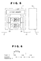
- Fig. 5 is a block diagram showing in detail the arrangement of the memory unit used in an embodiment of this invention which deals with two tasks, a task H being higher in priority than the task L.
- indicated by 25 is a flip-flop provided for the task H. It is assumed that the task H has an execution time of about 10 ms and it is initiated at an interval of about 30 ms.
- the master CPU 1 delivers the output data of the task H to the PIO unit 7 and sets the flip-flop 25.
- the master CPU 1 implements, during the period when the task H is not run, the execution of the task L, the delivery of the output data of the task L to the PIO unit 7, and the setting of the flip-flop 22.
- the data transfer unit 13 transfers the memory contents of the task H from the master's memory unit 11 to the slave's memory unit 12, and resets the flip-flop 25 on completion of the data transfer.
- the data transfer unit 13 responds to the setting of the flip-flop 22 to transfer the memory contents for the task L from the memory unit 11 to the memory unit 12, and then reset the flip-flop 22.
- the processing of the task H with the higher priority level has the precedence of the task L also in this case.
- This embodiment which enables the faster processing for the higher priority task, necessitates a memory guard function (not shown) as will be explained in the following.
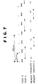
- the operational timing shown in Fig. 7 reveals that there is a significant restriction of communication between the task H and task L. A manner of alleviating the restriction will be explained with reference to the timing chart of Fig. 8.
- the task-H initiation command is issued at a 30 ms interval, with the task-L initiation command being issued simultaneously at every third issuance of the task-H initiation command, in the same manner as shown in Fig. 7.
- the CPU 1 responds to the completion of task H to deliver the output data produced in the task H to the PIO unit 7 and set the flip-flop 25. At this time, initiation of the task L is held until the transfer of the memory contents for the task H by the transfer unit 13 is completed.
- the subsequent process is identical to the manner shown in Fig. 7.
- Fig. 8 has a concurrent implementation of task execution and memory transfer only for the execution of task H and memory transfer for the task L, and it necessitates the exclusive memory write control only during the execution of task H, facilitating the communication between the task H and task L.
- the foregoing embodiment is the case of two kinds of tasks H and L, the number of kinds of tasks may be three or more.
- the processing apparatus is provided, in correspondence to a plurality of tasks, with memory units each incorporating flip-flops which are set in response to the completion of task execution of the master CPU and a data storage area, and when a flip-flop in the master's memory unit is set in response to the completion of task execution of the master CPU, data in the relevant memory area is transferred from the master's memory unit to the slave's memory unit and the flip-flop is reset on completion of data transfer so that the task can be initiated, whereby the data which has been transferred to the slave's memory unit is prevented from being destroyed in the event of disorder of the master CPU, and consequently the slave CPU which now takes control in place of the defective master CPU can surely back up the process with the normal data.
Landscapes
- Engineering & Computer Science (AREA)
- Theoretical Computer Science (AREA)
- Quality & Reliability (AREA)
- Physics & Mathematics (AREA)
- General Engineering & Computer Science (AREA)
- General Physics & Mathematics (AREA)
- Hardware Redundancy (AREA)
Claims (4)
- Verarbeitungsvorrichtung, die- eine erste zentrale Verarbeitungseinheit (1) und eine zweite zentrale Verarbeitungseinheit (2), wobei die zweite oder die erste zentrale Verarbeitungseinheit einen Betrieb beginnt, falls die erste bzw. zweite zentrale Verarbeitungseinheit während ihres Betriebs unbrauchbar wird;- eine erste Speichereinheit (11), die über einen ersten Bus mit der ersten zentralen Verarbeitungseinheit (1) verbunden ist, und einen zweiten Speicher (12), der über einen zweiten Bus mit der zweiten zentralen Verarbeitungseinheit (2) verbunden ist; und- eine Datenübertragungseinheit (13) aufweist, welche, wenn eine gegenwärtig arbeitende der ersten und zweiten zentralen Verarbeitungseinheiten (1, 2) in Übereinstimmung mit einem Vollenden eines Ausführens einer Aufgabe eine Reihe von Daten in die entsprechende der ersten und zweiten Speichereinheiten (11, 12) geschrieben hat, Daten, die in die Speichereinheit geschrieben worden sind, die der arbeitenden zentralen Verarbeitungseinheit entspricht, zu der Speichereinheit überträgt, die der gegenwärtig nicht arbeitenden zentralen Verarbeitungseinheit entspricht,dadurch gekennzeichnet, daß jede der ersten und zweiten Speichereinheiten (11, 12) aus- einem Zweitor-Speicher (21), der ein erstes Tor (3; 4) zum Datenzugriff durch die entsprechende zentrale Verarbeitungseinheit (1, 2) und ein zweites Tor (14) zum Datenzugriff durch die Datenübertragungseinheit (13) aufweist, und ebenso getrennte Datenspeicherbereiche aufweist, von denen jeder einer von einer Mehrzahl von Aufgaben (H, L) zugeordnet ist und in der Lage ist, getrennt zum Schreiben freigegeben zu werden, und während eines Übertragens in ihrer Gesamtheit, wie sie der jeweiligen Aufgabe zugeordnet sind, übertragen zu werden; und- einer Mehrzahl von Flipflops (22, 25) besteht, die den Aufgaben entsprechen, die durch die jeweilige arbeitende zentrale Verarbeitungseinheit (1; 2) ablaufen, wobei jedes der Flipflops (22, 25) durch die arbeitende zentrale Verarbeitungseinheit (1; 2), die eine entsprechende Aufgabe vollendet hat, gesetzt wird und nach einem Vollenden einer Datenübertragung von der Datenübertragungseinheit (13) zurückgesetzt wird.
- Verarbeitungsvorrichtung nach Anspruch 1, bei der die Datenübertragungseinheit (13) einen Zugriff zur Datenübertragung lediglich auf einen Datenspeicherbereich durchführt, der von einer Aufgabe (H, L) verwendet wird, die einem gesetzten der Flipflops (22, 25) entspricht.
- Verarbeitungsvorrichtung nach Anspruch 2, bei der die jeweilige arbeitende zentrale Verarbeitungseinheit (1, 2) nach einem Vollenden einer Aufgabe (H, L) und wenn es eine andere Aufgabe mit einem Bereitschaftszustand gibt, arbeitet, um die andere Aufgabe sofort ablaufen zu lassen.
- Verarbeitungsvorrichtung nach Anspruch 2, bei der die jeweilige arbeitende zentrale Verarbeitungseinheit (1, 2) nach einem Erfassen des Bereitschaftszustands einer Aufgabe mit niedrigerer Priorität bei dem Vollenden eines Ausführens einer Aufgabe mit höherer Priorität arbeitet, um die Aufgabe mit niedrigerer Priorität auszuführen, nachdem das Flipflop (22, 25), das der Aufgabe mit höherer Priorität entspricht, zurückgesetzt worden ist.
Applications Claiming Priority (4)
| Application Number | Priority Date | Filing Date | Title |
|---|---|---|---|
| JP113651/91 | 1991-04-19 | ||
| JP3113651A JPH04320539A (ja) | 1991-04-19 | 1991-04-19 | 演算装置 |
| JP156174/91 | 1991-05-31 | ||
| JP3156174A JPH04354048A (ja) | 1991-05-31 | 1991-05-31 | 演算装置のバックアップ方式 |
Publications (2)
| Publication Number | Publication Date |
|---|---|
| EP0509227A1 EP0509227A1 (de) | 1992-10-21 |
| EP0509227B1 true EP0509227B1 (de) | 1997-02-12 |
Family
ID=26452598
Family Applications (1)
| Application Number | Title | Priority Date | Filing Date |
|---|---|---|---|
| EP19920103999 Expired - Lifetime EP0509227B1 (de) | 1991-04-19 | 1992-03-09 | Verarbeitungseinrichtung mit Reserveprozessor |
Country Status (2)
| Country | Link |
|---|---|
| EP (1) | EP0509227B1 (de) |
| DE (1) | DE69217405T2 (de) |
Family Cites Families (3)
| Publication number | Priority date | Publication date | Assignee | Title |
|---|---|---|---|---|
| US4351023A (en) * | 1980-04-11 | 1982-09-21 | The Foxboro Company | Process control system with improved system security features |
| US4872106A (en) * | 1983-04-06 | 1989-10-03 | New Forney Corp. | Industrial process control system with back-up data processors to take over from failed primary data processors |
| US4959768A (en) * | 1989-01-23 | 1990-09-25 | Honeywell Inc. | Apparatus for tracking predetermined data for updating a secondary data base |
-
1992
- 1992-03-09 EP EP19920103999 patent/EP0509227B1/de not_active Expired - Lifetime
- 1992-03-09 DE DE1992617405 patent/DE69217405T2/de not_active Expired - Fee Related
Also Published As
| Publication number | Publication date |
|---|---|
| DE69217405D1 (de) | 1997-03-27 |
| EP0509227A1 (de) | 1992-10-21 |
| DE69217405T2 (de) | 1997-10-23 |
Similar Documents
| Publication | Publication Date | Title |
|---|---|---|
| US5021950A (en) | Multiprocessor system with standby function | |
| EP0524530B1 (de) | DMA-Steuerung | |
| US5125081A (en) | Inter-configuration changing controller based upon the connection and configuration information among plurality of clusters and the global storage | |
| EP0458304B1 (de) | Direktspeicherzugriffübertragungssystem und Benutzung | |
| EP0116344B1 (de) | Doppelspeichersystem mit Reservestromversorgung | |
| WO1994027224A1 (en) | Apparatus and method for automatic recognition and configuration of a peripheral device | |
| EP0013740B1 (de) | Datenverarbeitungsgerät mit Rückstellvorrichtung für das System | |
| EP0239078B1 (de) | System zur Registersicherstellung/-umspeicherung | |
| EP0055623B1 (de) | Direkter Speicherzugriffbetrieb für ein Speichersystem mit hoher Geschwindigkeit | |
| JPH08320835A (ja) | 外部バスの障害検出方法 | |
| US6184904B1 (en) | Central processing unit for a process control system | |
| EP0509227B1 (de) | Verarbeitungseinrichtung mit Reserveprozessor | |
| US6209001B1 (en) | Back-up system capable of performing back-up operation at optional time | |
| EP1410186A2 (de) | Interrupt-steuerung für einen mikroprozessor | |
| KR100428798B1 (ko) | 슬레이브 초기화 장치 | |
| JPH0827761B2 (ja) | 二重化メモリの両系同時書込方法 | |
| RU1820391C (ru) | Многопроцессорна вычислительна система | |
| JPH05307491A (ja) | 多重化処理装置の切替方法および装置 | |
| JPH04320539A (ja) | 演算装置 | |
| JP3033640B2 (ja) | Cpu動作監視回路 | |
| JPH07114521A (ja) | マルチマイクロコンピュータシステム | |
| JPS6127793B2 (de) | ||
| JPH0668011A (ja) | Scsiインターフェース装置 | |
| JP3661609B2 (ja) | Scsiインタフェース制御装置およびそのセレクション監視方法 | |
| JP2640139B2 (ja) | メモリカード |
Legal Events
| Date | Code | Title | Description |
|---|---|---|---|
| PUAI | Public reference made under article 153(3) epc to a published international application that has entered the european phase |
Free format text: ORIGINAL CODE: 0009012 |
|
| AK | Designated contracting states |
Kind code of ref document: A1 Designated state(s): DE FR GB |
|
| 17P | Request for examination filed |
Effective date: 19930413 |
|
| 17Q | First examination report despatched |
Effective date: 19951123 |
|
| GRAG | Despatch of communication of intention to grant |
Free format text: ORIGINAL CODE: EPIDOS AGRA |
|
| GRAH | Despatch of communication of intention to grant a patent |
Free format text: ORIGINAL CODE: EPIDOS IGRA |
|
| GRAH | Despatch of communication of intention to grant a patent |
Free format text: ORIGINAL CODE: EPIDOS IGRA |
|
| GRAA | (expected) grant |
Free format text: ORIGINAL CODE: 0009210 |
|
| AK | Designated contracting states |
Kind code of ref document: B1 Designated state(s): DE FR GB |
|
| REF | Corresponds to: |
Ref document number: 69217405 Country of ref document: DE Date of ref document: 19970327 |
|
| ET | Fr: translation filed | ||
| REG | Reference to a national code |
Ref country code: GB Ref legal event code: 727 |
|
| REG | Reference to a national code |
Ref country code: GB Ref legal event code: 727H |
|
| REG | Reference to a national code |
Ref country code: GB Ref legal event code: SP |
|
| PLBE | No opposition filed within time limit |
Free format text: ORIGINAL CODE: 0009261 |
|
| STAA | Information on the status of an ep patent application or granted ep patent |
Free format text: STATUS: NO OPPOSITION FILED WITHIN TIME LIMIT |
|
| 26N | No opposition filed | ||
| REG | Reference to a national code |
Ref country code: GB Ref legal event code: 746 Effective date: 19990519 |
|
| REG | Reference to a national code |
Ref country code: FR Ref legal event code: D6 |
|
| REG | Reference to a national code |
Ref country code: GB Ref legal event code: IF02 |
|
| PGFP | Annual fee paid to national office [announced via postgrant information from national office to epo] |
Ref country code: FR Payment date: 20020312 Year of fee payment: 11 |
|
| PGFP | Annual fee paid to national office [announced via postgrant information from national office to epo] |
Ref country code: GB Payment date: 20020313 Year of fee payment: 11 |
|
| PGFP | Annual fee paid to national office [announced via postgrant information from national office to epo] |
Ref country code: DE Payment date: 20020327 Year of fee payment: 11 |
|
| PG25 | Lapsed in a contracting state [announced via postgrant information from national office to epo] |
Ref country code: GB Free format text: LAPSE BECAUSE OF NON-PAYMENT OF DUE FEES Effective date: 20030309 |
|
| PG25 | Lapsed in a contracting state [announced via postgrant information from national office to epo] |
Ref country code: DE Free format text: LAPSE BECAUSE OF NON-PAYMENT OF DUE FEES Effective date: 20031001 |
|
| GBPC | Gb: european patent ceased through non-payment of renewal fee |
Effective date: 20030309 |
|
| PG25 | Lapsed in a contracting state [announced via postgrant information from national office to epo] |
Ref country code: FR Free format text: LAPSE BECAUSE OF NON-PAYMENT OF DUE FEES Effective date: 20031127 |
|
| REG | Reference to a national code |
Ref country code: FR Ref legal event code: ST |