EP0506397B1 - Dispositif pour mesurer une forme d'onde optique - Google Patents
Dispositif pour mesurer une forme d'onde optique Download PDFInfo
- Publication number
- EP0506397B1 EP0506397B1 EP92302621A EP92302621A EP0506397B1 EP 0506397 B1 EP0506397 B1 EP 0506397B1 EP 92302621 A EP92302621 A EP 92302621A EP 92302621 A EP92302621 A EP 92302621A EP 0506397 B1 EP0506397 B1 EP 0506397B1
- Authority
- EP
- European Patent Office
- Prior art keywords
- light
- measured
- optical pulse
- pulse
- sampling
- Prior art date
- Legal status (The legal status is an assumption and is not a legal conclusion. Google has not performed a legal analysis and makes no representation as to the accuracy of the status listed.)
- Expired - Lifetime
Links
Images

Classifications
-
- G—PHYSICS
- G01—MEASURING; TESTING
- G01J—MEASUREMENT OF INTENSITY, VELOCITY, SPECTRAL CONTENT, POLARISATION, PHASE OR PULSE CHARACTERISTICS OF INFRARED, VISIBLE OR ULTRAVIOLET LIGHT; COLORIMETRY; RADIATION PYROMETRY
- G01J11/00—Measuring the characteristics of individual optical pulses or of optical pulse trains
Definitions
- the present invention relates to an optical waveform measuring device and is suitable for measuring an optical waveform of, e.g. a high-speed optical pulse, by using a light sampling method.
- an optical waveform measuring device there are (a) a measuring device as a combination of a photodetector, e.g., a photodiode or a photomultiplier tube (to be referred to as a PMT hereinafter) and an oscilloscope, (b) a measuring device using a streak camera, and (c) a measuring device using light-light sampling by generation of a sum frequency.
- a photodetector e.g., a photodiode or a photomultiplier tube (to be referred to as a PMT hereinafter) and an oscilloscope
- a measuring device using a streak camera e.g., a measuring device using a streak camera
- the measuring device as a combination of the photodetector and the oscilloscope, a high time-resolution cannot be obtained (the time resolution is as low as several 10 pS), and a waveform distortion occurs.
- the measuring device using the streak camera the measuring device becomes expensive.
- the measuring device using light-light sampling a nonlinear optical crystal is necessary for generation of the sum frequency. However, this crystal is difficult to handle because it is deliquescent. Furthermore, phase matching must be performed when light is to be incident on this crystal, and the crystal itself is expensive.
- the present invention aims to provide a high-resolution, simple optical waveform measuring device which does not need a nonlinear optical crystal that has problems in handling.
- the present invention also aims to provide an optical waveform measuring device comprising photoelectric converting means including a part having a function of generating one photoelectron upon absorption of one photon within a predetermined wavelength range, and a pulse light source for generating a sampling optical pulse having a predetermined wavelength outside the predetermined wavelength range.
- an optical waveform measuring device comprising: photoelectric converting means, including generating means for generating a photo-electron upon absorption of plural photons each of a respective wavelength above a predetermined wavelength, for receiving light to be measured of a wavelength above the predetermined wavelength the predetermined wavelength corresponding to the upper limit of the sensitivity range of the photoelectric converting means, in which range one photoelectron is generated upon absorption of one photon characterised by: a pulse light source for generating a sampling optical pulse of a wavelength above said predetermined wavelength to be received by said photoelectric converting means so as to cause the same to output a signal corresponding to the generation of a photoelectron upon absorption of plural photons by said generating means when the light to be measured and the sampling optical pulse are simultaneously incident on said generating means.
- the photoelectric converting means outputs a signal corresponding to generation of one photoelectron upon multiphoton absorption within the part when light to be measured and the sampling optical pulse are simultaneously incident on the same position of the part.
- the number of photoelectrons generated by the part corresponds to the product of the intensities of the light to be measured and the sampling optical pulse.
- the number of the photoelectron emitted from the photocathode of the electron tube does not only correspond to the intensity of the sampling optical pulse but corresponds to the product of the intensities of the light to be measured and the sampling optical pulse.
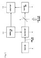
- a measuring device shown in Fig. 1 can use various types of devices, e.g., an electron tube or a photoconductive device as a photoelectric converting unit for light-light sampling.
- a measuring device which uses an electron tube as the photoelectric converting unit will be described below.
- the photocathode of a multiphoton-absorption (or nonlinear) electron tube 2 emits one photoelectron upon absorption of one photon having a wavelength within a predetermined wavelength band (an ordinary sensitivity range of the photocathode).
- the photocathode of the electron tube 2 does not substantially have the sensitivity to emit one photoelectron upon absorption of one photon. If the wavelength of the incident light is longer than the upper wavelength limit of the sensitivity of the photocathode of the electron tube 2, one photoelectron is emitted upon incidence of two or more photons. Light-light sampling is enabled by this multi-photon absorption and one-photoelectron emission, which will be described below.
- An optical pulse generating unit 4 generates a sampling optical pulse having a longer wavelength than the upper wavelength limit of the sensitivity of the photocathode.
- a delaying unit 6 changes the incident timing of the sampling optical pulse on the electron tube 2 in synchronism with the incident timing of light to be measured on the electron tube 2.
- a half mirror 8 guides the sampling optical pulse passing through the delaying unit 6 and the external light to be measured to the photocathode of the electron tube 2 such that they overlap each other on the photocathode.
- An output signal (sampling output) from the electron tube 2 corresponds to the incident intensity of the measured light at the incident timing of the sampling optical pulse.
- the sampling output from the electron tube 2 is input to a display unit 10, e.g., an oscilloscope.
- a controlling unit 12 controls the delaying unit 6 to sequentially and gradually shift the incident timing of the sampling optical pulse on the electron tube 2 and controls the operation of the display unit 10 in synchronism with the sampling optical pulse.
- a series of sampling outputs from the electron tube 2 can be converted to an optical waveform of the light to be measured and displayed on the display unit 10.
- Fig. 1 The operation of the measuring device shown in Fig. 1 will be described. While the pulse of light to be measured having an arbitrary wavelength is incident on the photocathode of the electron tube 2, when a relatively short sampling optical pulse is incident on the same position of the photocathode at a controlled incident timing, one photoelectron is emitted upon incidence of, e.g., two photons of the light to be measured and the sampling optical pulse. An electric signal corresponding to this photoelectron is output from the electron tube 2 as a sampling output.
- a sampling output proportional to the square of the sum of the incident intensity of the light to be measured and the incident intensity of the sampling optical pulse
- the incident intensity of the light to be measured when the light to be measured and the sampling optical pulse overlap, can be detected by arbitrarily processing this sampling output. That is, even in the method of using the photocathode as described above, an effect similar to that of light-light sampling using a method of generating second harmonics by using a nonlinear optical crystal can be obtained.
- the controlling unit 12 causes repetition of this light-light sampling by arbitrarily shifting the incident timing of the sampling optical pulse by the delaying unit 6.
- the profile of the optical waveform of the light to be measured can be obtained by enveloping or plotting the results of light-light sampling of the optical waveform of the light to be measured at different timings, and this profile can be displayed on the display unit 10. Since this method is based on the mutual relationship between the intensity of the sampling optical pulse and the intensity of the pulse of the light to be measured, the output from the electron tube need be integrated over a sufficiently long period of time when compared to the time width of the pulse of the light to be measured. In other words, the corresponding band of the electron tube need not be wide.
- the material of the photocathode of the electron tube 2 e.g., Au or CsI can be used. If the photocathode is made of CsI, when each of the sampling optical pulse and the light to be measured has a wavelength of about 600 nm, a sampling output proportional to the square of the sum of the incident intensity of the sampling optical pulse and the incident intensity of the light to be measured can be obtained. If the photocathode is made of Au, when the sampling optical pulse and the light to be measured are ultraviolet rays, a sampling output (nonlinear output) proportional to the square of the sum of the incident intensity of the sampling optical pulse and the incident intensity of the light to be measured can be obtained.
- a signal proportional to the intensity of the light to be measured at the incident timing of the sampling optical pulse can be obtained by removing the background component (the sum of the time integral of the square of the incident intensity of the sampling optical pulse and the time integral of the square of the incident intensity of the light to be measured) from the sampling output.
- intensity detection of the light to be measured at different timings is enabled.
- the profile of the optical waveform of the light to be measured can be obtained by enveloping or plotting the detected intensities of the light to be measured.
- the background component is removed from the sampling output. Then, a signal corresponding to the intensity of the light to be measured at the incident timing of the sampling optical pulse, or a signal proportional to the square of this intensity can be obtained, in accordance with a ratio of the intensity of the sampling optical pulse to that of the light to be measured.
- the optical waveform of the light to be measured can be measured in the same manner as described above.
- a phototube, a PMT, or the like can be used as the electron tube 2.
- a PMT measurement with a high S/N ratio is enabled.
- a photoconductive device which generates a nonlinear output upon absorption of two photons can be used in place of the electron tube.
- the two-photon process of a semiconductor device will be briefly described.
- the valence band is excited by either one of the photons to emit one electron.
- the one electron is raised to a certain level of the forbidden band and then raised to the conduction band by the other photon through the temporary intermediate state. That is, two photons are absorbed by one valance electron to generate one free electron. This indicates that two-photon absorption is caused when pulsed optical beams each having a wavelength not reaching an ordinarily utilized detection spectrum range are caused to be incident on the photosensitive region of the semiconductor device.
- the number of free electrons generated by the above phenomenon corresponds to the product of the intensities of the light to be measured and the sampling optical pulse.
- light-light sampling without using a nonlinear optical element is enabled by observing the output from the semiconductor device.
- a GaAsP photodiode, a CdS photocell, an Si photodiode, or the like can be used as such a semiconductor device.
- Any laser e.g., a solid-state laser, a dye laser, a gas laser, or a semiconductor laser can be used as the optical pulse generating unit 4 as far as it generates short pulse light.
- the incident timings of the sampling optical pulse and the light to be measured may be controlled by changing the incident timing of the light to be measured on the photocathode but not changing the incident timing of the sampling optical pulse on the photocathode.
- an optical amplifier for amplifying the light to be measured is connected to the input of the electron tube 2 to cause the amplified high-intensity light to be incident on the electron tube 2, measurement with a higher S/N ratio can be performed.
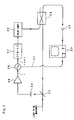
- Fig. 2 is a schematic diagram of the arrangement of the measuring device according to the first embodiment of the present invention.
- Part of light to be measured which is incident on a half mirror 22 is transmitted through this mirror 22 and guided to one input terminal of a single-mode fiber coupler (to be referred as an SMF coupler hereinafter) 23.
- the rest of the light to be measured is reflected by the half mirror 22 and is incident on a PMT 24.
- the PMT 24 has an ordinary sensitivity of one-photon absorption and one-photoelectron emission with respect to light to be measured.
- the light to be measured is linearly converted to an electrical signal by the PMT 24 and amplified by an amplifier 25.
- the electrical signal is frequency-modulated by f by a frequency modulating unit 26.
- an electrical signal having a repetition frequency f+ ⁇ f, where ⁇ f is the repetition frequency of the light to be measured is generated.
- a distributed feedback (DFB) laser diode 27 is excited by this electrical signal to generate a monochromatic light pulse having a repetition frequency f+ ⁇ f by its gain switching.
- the pulse width of the monochromatic light pulse is compressed by a pulse compressor 28 comprising, e.g., a fiber, thus obtaining a sampling optical pulse having a very short pulse width compared to the pulse width of the light to be measured.
- This sampling optical pulse is multiplexed with the light to be measured by the SMF coupler 23 and is incident on a nonlinear PMT 29.
- a sampling output proportional to the square of the sum of their incident intensities can be obtained.
- the sampling output is input to an oscilloscope 30, and the electrical signal having the repetition frequency ⁇ f is also input to the oscilloscope 30 from the frequency modulating unit 26.
- the optical waveform of the light to be measured can be displayed on the oscilloscope 30 by repeatedly sweeping the AC component of the sampling output at the repetition frequency ⁇ f.
- Fig. 3 schematically shows the arrangement of a measuring device according to the second embodiment of the present invention.
- Short pulse light from, e.g., a CPM ring laser, a YAG laser, or a YAG-pumping dye laser is incident on a half mirror M1.
- Part of the short pulse light incident on the half mirror M1 is reflected by this mirror M1, reflected by mirrors M6, M7, and M8 again, and is incident on a sample cell 36 as the pumping light.
- the pumping light incident on the sample cell 36 excites the material to be measured inside the sample cell 36 to generate fluorescence.
- the fluorescence emerging from the sample cell 36 is incident on a condenser lens 38.
- the rest of the short pulse light is transmitted through the half mirror M1 to linearly propagate as the sampling optical pulse and is incident on a mirror M2.
- the sampling optical pulse reflected by the mirror M2 reciprocates between the mirrors M2, M3 and a movable prism 32 to be delayed by an arbitrarily period of time and is then incident on the condenser lens 38 through mirrors M3, M4, and M5.
- a controller 33 displaces the movable prism 32 to control the delay time of the sampling optical pulse.
- the controller 33 also supplies a scanning signal corresponding to the delay time of the sampling optical pulse to an X-axis input terminal of an oscilloscope 34.
- the sampling optical pulse and the fluorescence incident on the condenser lens 38 are incident on a nonlinear PMT 39.
Landscapes
- Physics & Mathematics (AREA)
- General Physics & Mathematics (AREA)
- Spectroscopy & Molecular Physics (AREA)
- Photometry And Measurement Of Optical Pulse Characteristics (AREA)
Claims (26)
- Dispositif de mesure de forme d'onde optique comportant :des moyens de conversion photoélectriques (2, 29, 39), comportant des moyens de production pour produire un photoélectron lors de l'absorption de plusieurs photons ayant chacun une longueur d'onde respective supérieure a une longueur d'onde prédéterminée, pour recevoir une lumière à mesurer ayant une longueur d'onde supérieure à la longueur d'onde prédéterminée, la longueur d'onde prédéterminée correspondant à la limite supérieure de la plage de sensibilités des moyens de conversion photoélectriques, plage dans laquelle un photoélectron est produit lors de l'absorption d'un photon,caractérisé en ce qu'il comporte :une source d'impulsions lumineuses (4, 6, 24 à 28, 32, M1 à M5) destinée à produire une impulsion optique d'échantillonnage ayant une longueur d'onde supérieure à ladite longueur d'onde prédéterminée à recevoir par lesdits moyens de conversion photoélectriques, de manière à les amener à émettre un signal correspondant à la production d'un photoélectron lors de l'absorption de plusieurs photons par lesdits moyens de production lorsque la lumière à mesurer et l'impulsion optique d'échantillonnage sont incidentes simultanément sur lesdits moyens de production.
- Dispositif selon la revendication 1, dans lequel lesdits moyens de conversion photoélectriques sont constitués d'un tube électronique (2) ayant une photocathode en tant que dits moyens de production.
- Dispositif selon la revendication 2, dans lequel ledit tube électronique est un tube photomultiplicateur.
- Dispositif selon la revendication 2 ou 3, dans lequel ladite photocathode est constituée d'Au.
- Dispositif selon l'une quelconque des revendications précédentes, dans lequel l'impulsion optique d'échantillonnage et la lumière à mesurer ont une longueur d'onde de l'ordre de 600 nm.
- Dispositif selon l'une quelconque des revendications 1 à 3, dans lequel ladite photocathode est constituée de CsI.
- Dispositif selon la revendication 6, dans lequel l'impulsion optique d'échantillonnage et la lumière à mesurer sont des rayons ultraviolets.
- Dispositif selon l'une quelconque des revendications précédentes, dans lequel lesdits moyens de conversion photoélectriques (29, 39) sont constitués d'un dispositif à semi-conducteur ayant une zone photosensible en tant que dits moyens de production.
- Dispositif selon la revendication 8, dans lequel ledit dispositif à semi-conducteur est un dispositif photoconducteur.
- Dispositif selon la revendication 8, dans lequel ledit dispositif à semi-conducteur est une photodiode.
- Dispositif selon l'une quelconque des revendications précédentes, comportant en outre des moyens optiques (8, 23, 38) pour guider la lumière à mesurer et l'impulsion optique d'échantillonnage, de sorte que celles-ci se superposent l'une à l'autre à l'intérieur desdits moyens de production.
- Dispositif selon la revendication 11, dans lequel lesdits moyens optiques comportent un connecteur de fibres (23).
- Dispositif selon la revendication 11, dans lequel lesdits moyens optiques comportent une lentille (38).
- Dispositif selon l'une quelconque des revendications précédentes, comportant en outre des moyens à retard (24 à 28) pour faire varier l'instant d'incidence de la lumière à mesurer sur lesdits moyens de production en correspondance avec l'instant d'incidence de l'impulsion optique d'échantillonnage sur lesdits moyens de production.
- Dispositif selon l'une quelconque des revendications 1 à 14, comportant en outre des moyens à retard (M1 à M5, 32) pour faire varier l'instant d'incidence de l'impulsion optique d'échantillonnage sur lesdits moyens de production en correspondance avec l'instant d'incidence de la lumière à mesurer sur lesdits moyens de production.
- Dispositif selon la revendication 14, dans lequel lesdits moyens à retard sont un modulateur de fréquence (26) destiné à convertir une fréquence de répétition de la lumière à mesurer en une fréquence plus élevée.
- Dispositif selon la revendication 15, dans lequel lesdits moyens à retard sont un miroir mobile (32) destiné à augmenter ou à diminuer le chemin optique de l'impulsion optique d'échantillonnage.
- Dispositif selon l'une quelconque des revendications précédentes, dans lequel ladite source d'impulsions lumineuses est un laser à semi-conducteur.
- Dispositif selon l'une quelconque des revendications 1 à 18, dans lequel ladite source d'impulsions lumineuses est un laser à colorant.
- Dispositif selon l'une quelconque des revendications 1 à 18, dans lequel ladite source d'impulsions lumineuses est un laser solide.
- Dispositif selon l'une quelconque des revendications 1 à 18, dans lequel ladite source d'impulsions lumineuses est un laser à gaz.
- Dispositif selon la revendication 15, dans lequel lesdits moyens à retard sont un modulateur de fréquence (26) destiné à convertir une fréquence de répétition de la lumière à mesurer en une fréquence plus élevée, et ladite source d'impulsions lumineuses est un laser à semi-conducteur destiné à produire l'impulsion optique d'échantillonnage en réponse à un signal provenant desdits moyens à retard.
- Dispositif selon l'une quelconque des revendications précédentes, comportant en outre des moyens d'affichage (10, 30, 34) pour afficher de manière analytique le signal provenant desdits moyens de conversion photoélectriques (2, 29, 39).
- Dispositif selon l'une quelconque des revendications précédentes, comportant en outre des moyens (22) pour découper la lumière à mesurer ou l'impulsion optique d'échantillonnage et un amplificateur synchrone (25) pour amplifier de manière synchrone le signal provenant desdits moyens de conversion photoélectriques.
- Dispositif selon l'une quelconque des revendications précédentes, comportant en outre un amplificateur optique (36) destiné à amplifier la lumière à mesurer, relié au côté entrée des moyens de conversion photoélectriques.
- Dispositif selon la revendication 14, comportant en outre des moyens de commande (33) pour commander lesdits moyens à retard (M1 à M5, 32) afin de décaler de manière graduelle l'instant d'incidence de l'impulsion optique d'échantillonnage, et des moyens à retard (34) pour envelopper les signaux provenant desdits moyens de conversion photoélectriques à chaque instant d'incidence de l'impulsion optique d'échantillonnage et pour afficher les signaux enveloppés correspondant à la forme d'onde de la lumière à mesurer.
Applications Claiming Priority (2)
| Application Number | Priority Date | Filing Date | Title |
|---|---|---|---|
| JP63433/91 | 1991-03-27 | ||
| JP06343391A JP3176644B2 (ja) | 1991-03-27 | 1991-03-27 | 光波形の測定装置 |
Publications (3)
| Publication Number | Publication Date |
|---|---|
| EP0506397A2 EP0506397A2 (fr) | 1992-09-30 |
| EP0506397A3 EP0506397A3 (en) | 1993-02-03 |
| EP0506397B1 true EP0506397B1 (fr) | 1996-05-29 |
Family
ID=13229139
Family Applications (1)
| Application Number | Title | Priority Date | Filing Date |
|---|---|---|---|
| EP92302621A Expired - Lifetime EP0506397B1 (fr) | 1991-03-27 | 1992-03-26 | Dispositif pour mesurer une forme d'onde optique |
Country Status (4)
| Country | Link |
|---|---|
| US (1) | US5168164A (fr) |
| EP (1) | EP0506397B1 (fr) |
| JP (1) | JP3176644B2 (fr) |
| DE (1) | DE69211042T2 (fr) |
Families Citing this family (8)
| Publication number | Priority date | Publication date | Assignee | Title |
|---|---|---|---|---|
| CN1037126C (zh) * | 1994-08-30 | 1998-01-21 | 中国科学院上海光学精密机械研究所 | 激光脉冲信噪比测试仪 |
| US5682038A (en) * | 1995-04-06 | 1997-10-28 | Becton Dickinson And Company | Fluorescent-particle analyzer with timing alignment for analog pulse subtraction of fluorescent pulses arising from different excitation locations |
| FR2749721B1 (fr) * | 1996-06-07 | 1998-11-27 | Thomson Csf | Commutateur electrique a photoconducteur |
| US6891363B2 (en) * | 2002-09-03 | 2005-05-10 | Credence Systems Corporation | Apparatus and method for detecting photon emissions from transistors |
| US6943572B2 (en) * | 2002-09-03 | 2005-09-13 | Credence Systems Corporation | Apparatus and method for detecting photon emissions from transistors |
| JP2005164350A (ja) | 2003-12-02 | 2005-06-23 | Yokogawa Electric Corp | 電子ビーム発生装置及びこの装置を用いた光サンプリング装置 |
| JP5203063B2 (ja) * | 2008-06-24 | 2013-06-05 | オリンパス株式会社 | 多光子励起測定装置 |
| US8630036B2 (en) * | 2009-10-30 | 2014-01-14 | Deep Photonics Corporation | Method and system using phase modulation to reduce spectral broadening |
Family Cites Families (9)
| Publication number | Priority date | Publication date | Assignee | Title |
|---|---|---|---|---|
| US4661694A (en) * | 1985-09-13 | 1987-04-28 | Corcoran Vincent J | Infrared streak camera |
| JP2665231B2 (ja) * | 1988-05-13 | 1997-10-22 | 浜松ホトニクス株式会社 | 光波形測定装置 |
| JPH0617819B2 (ja) * | 1988-05-13 | 1994-03-09 | 浜松ホトニクス株式会社 | 電気光学式ストリークカメラ |
| JPH0758376B2 (ja) * | 1988-05-26 | 1995-06-21 | 浜松ホトニクス株式会社 | 光波形整形装置 |
| JP2659554B2 (ja) * | 1988-05-30 | 1997-09-30 | 浜松ホトニクス株式会社 | 光強度相関装置 |
| JPH0769351B2 (ja) * | 1988-05-30 | 1995-07-26 | 浜松ホトニクス株式会社 | 電気信号観測装置 |
| US5071249A (en) * | 1988-10-05 | 1991-12-10 | Hamamatsu Photonics K.K. | Light waveform measuring apparatus |
| GB2226631B (en) * | 1988-12-28 | 1992-10-21 | Hamamatsu Photonics Kk | Optical waveform observing apparatus |
| JPH0670612B2 (ja) * | 1989-03-08 | 1994-09-07 | 浜松ホトニクス株式会社 | ストリークカメラ装置 |
-
1991
- 1991-03-27 JP JP06343391A patent/JP3176644B2/ja not_active Expired - Fee Related
-
1992
- 1992-03-26 DE DE69211042T patent/DE69211042T2/de not_active Expired - Fee Related
- 1992-03-26 EP EP92302621A patent/EP0506397B1/fr not_active Expired - Lifetime
- 1992-03-27 US US07/858,861 patent/US5168164A/en not_active Expired - Fee Related
Also Published As
| Publication number | Publication date |
|---|---|
| DE69211042D1 (de) | 1996-07-04 |
| JPH04297836A (ja) | 1992-10-21 |
| JP3176644B2 (ja) | 2001-06-18 |
| US5168164A (en) | 1992-12-01 |
| EP0506397A3 (en) | 1993-02-03 |
| DE69211042T2 (de) | 1996-10-24 |
| EP0506397A2 (fr) | 1992-09-30 |
Similar Documents
| Publication | Publication Date | Title |
|---|---|---|
| GB2231958A (en) | Measuring fluorescence characteristics | |
| US4461572A (en) | Instrument for measuring light emission induced by repetitive stimulation of the same type | |
| EP0506397B1 (fr) | Dispositif pour mesurer une forme d'onde optique | |
| US4988859A (en) | Optical waveform measuring device | |
| US5032714A (en) | Light waveform measuring device including a streak camera | |
| JPS61266942A (ja) | 2次元微弱発光測定装置 | |
| US3547542A (en) | High scanning speed spectrometer | |
| US5071249A (en) | Light waveform measuring apparatus | |
| JP2680398B2 (ja) | 光波形測定装置 | |
| US5308971A (en) | Measurement apparatus and techniques for ultrashort events using electron photoemission with a superlinear photoemission active element | |
| JP2525893B2 (ja) | 螢光特性検査装置 | |
| Tsuchiya et al. | Infrared sensitive universal streak camera for use in 1.0 to 1.6 µm wavelength region | |
| JPH0262806B2 (fr) | ||
| JP6684495B2 (ja) | 吸光分析装置 | |
| Nadeev et al. | Comparison of an avalanche photodiode and a photomultiplier tube as photodetectors of near-infrared radiation in the photon-counting mode | |
| GB2172991A (en) | Concurrently measuring a plurality of light signals | |
| JP2656106B2 (ja) | 光波形測定装置 | |
| SU972341A1 (ru) | Фотометр | |
| JPH0315745A (ja) | 光波形測定装置 | |
| GB2224352A (en) | Light waveform measuring apparatus | |
| JP2991260B2 (ja) | 時間分解発光測定装置 | |
| JP4452049B2 (ja) | 時間分解二次元微弱光検出方法および装置 | |
| JPH02234050A (ja) | 光波形測定装置 | |
| SU101678A1 (ru) | Импульсный фотометр | |
| JPH0315744A (ja) | 光波形測定装置 |
Legal Events
| Date | Code | Title | Description |
|---|---|---|---|
| PUAI | Public reference made under article 153(3) epc to a published international application that has entered the european phase |
Free format text: ORIGINAL CODE: 0009012 |
|
| AK | Designated contracting states |
Kind code of ref document: A2 Designated state(s): DE FR GB |
|
| PUAL | Search report despatched |
Free format text: ORIGINAL CODE: 0009013 |
|
| AK | Designated contracting states |
Kind code of ref document: A3 Designated state(s): DE FR GB |
|
| 17P | Request for examination filed |
Effective date: 19930630 |
|
| 17Q | First examination report despatched |
Effective date: 19941104 |
|
| GRAH | Despatch of communication of intention to grant a patent |
Free format text: ORIGINAL CODE: EPIDOS IGRA |
|
| GRAA | (expected) grant |
Free format text: ORIGINAL CODE: 0009210 |
|
| AK | Designated contracting states |
Kind code of ref document: B1 Designated state(s): DE FR GB |
|
| ET | Fr: translation filed | ||
| REF | Corresponds to: |
Ref document number: 69211042 Country of ref document: DE Date of ref document: 19960704 |
|
| PLBE | No opposition filed within time limit |
Free format text: ORIGINAL CODE: 0009261 |
|
| STAA | Information on the status of an ep patent application or granted ep patent |
Free format text: STATUS: NO OPPOSITION FILED WITHIN TIME LIMIT |
|
| 26N | No opposition filed | ||
| PGFP | Annual fee paid to national office [announced via postgrant information from national office to epo] |
Ref country code: DE Payment date: 20010319 Year of fee payment: 10 |
|
| REG | Reference to a national code |
Ref country code: GB Ref legal event code: IF02 |
|
| PG25 | Lapsed in a contracting state [announced via postgrant information from national office to epo] |
Ref country code: DE Free format text: LAPSE BECAUSE OF NON-PAYMENT OF DUE FEES Effective date: 20021001 |
|
| PGFP | Annual fee paid to national office [announced via postgrant information from national office to epo] |
Ref country code: FR Payment date: 20060308 Year of fee payment: 15 |
|
| PGFP | Annual fee paid to national office [announced via postgrant information from national office to epo] |
Ref country code: GB Payment date: 20060322 Year of fee payment: 15 |
|
| GBPC | Gb: european patent ceased through non-payment of renewal fee |
Effective date: 20070326 |
|
| REG | Reference to a national code |
Ref country code: FR Ref legal event code: ST Effective date: 20071130 |
|
| PG25 | Lapsed in a contracting state [announced via postgrant information from national office to epo] |
Ref country code: GB Free format text: LAPSE BECAUSE OF NON-PAYMENT OF DUE FEES Effective date: 20070326 |
|
| PG25 | Lapsed in a contracting state [announced via postgrant information from national office to epo] |
Ref country code: FR Free format text: LAPSE BECAUSE OF NON-PAYMENT OF DUE FEES Effective date: 20070402 |