EP0506380B1 - Appareil de traitement d'images - Google Patents
Appareil de traitement d'images Download PDFInfo
- Publication number
- EP0506380B1 EP0506380B1 EP92302597A EP92302597A EP0506380B1 EP 0506380 B1 EP0506380 B1 EP 0506380B1 EP 92302597 A EP92302597 A EP 92302597A EP 92302597 A EP92302597 A EP 92302597A EP 0506380 B1 EP0506380 B1 EP 0506380B1
- Authority
- EP
- European Patent Office
- Prior art keywords
- data
- subject pixel
- luminance
- image data
- pixels
- Prior art date
- Legal status (The legal status is an assumption and is not a legal conclusion. Google has not performed a legal analysis and makes no representation as to the accuracy of the status listed.)
- Expired - Lifetime
Links
- 238000012545 processing Methods 0.000 title claims description 18
- 238000000034 method Methods 0.000 claims description 45
- 238000009499 grossing Methods 0.000 claims description 30
- 230000002093 peripheral effect Effects 0.000 claims description 20
- 238000006243 chemical reaction Methods 0.000 claims description 18
- 238000003672 processing method Methods 0.000 claims 1
- 238000010586 diagram Methods 0.000 description 13
- 230000008030 elimination Effects 0.000 description 7
- 238000003379 elimination reaction Methods 0.000 description 7
- 239000011159 matrix material Substances 0.000 description 6
- 239000000872 buffer Substances 0.000 description 3
- 230000003111 delayed effect Effects 0.000 description 3
- 230000002542 deteriorative effect Effects 0.000 description 3
- 230000000694 effects Effects 0.000 description 3
- 238000001914 filtration Methods 0.000 description 3
- 230000001934 delay Effects 0.000 description 2
- 230000006870 function Effects 0.000 description 2
- 238000012935 Averaging Methods 0.000 description 1
- 238000003705 background correction Methods 0.000 description 1
- HPNSNYBUADCFDR-UHFFFAOYSA-N chromafenozide Chemical compound CC1=CC(C)=CC(C(=O)N(NC(=O)C=2C(=C3CCCOC3=CC=2)C)C(C)(C)C)=C1 HPNSNYBUADCFDR-UHFFFAOYSA-N 0.000 description 1
- 238000007796 conventional method Methods 0.000 description 1
- 230000003247 decreasing effect Effects 0.000 description 1
- 230000006866 deterioration Effects 0.000 description 1
- 230000003287 optical effect Effects 0.000 description 1
Images

Classifications
-
- H—ELECTRICITY
- H04—ELECTRIC COMMUNICATION TECHNIQUE
- H04N—PICTORIAL COMMUNICATION, e.g. TELEVISION
- H04N1/00—Scanning, transmission or reproduction of documents or the like, e.g. facsimile transmission; Details thereof
- H04N1/40—Picture signal circuits
- H04N1/409—Edge or detail enhancement; Noise or error suppression
- H04N1/4092—Edge or detail enhancement
-
- H—ELECTRICITY
- H04—ELECTRIC COMMUNICATION TECHNIQUE
- H04N—PICTORIAL COMMUNICATION, e.g. TELEVISION
- H04N1/00—Scanning, transmission or reproduction of documents or the like, e.g. facsimile transmission; Details thereof
- H04N1/40—Picture signal circuits
- H04N1/409—Edge or detail enhancement; Noise or error suppression
Definitions
- the present invention relates to an image processing apparatus capable of eliminating noises contained in image signals.
- An image processing apparatus has been used which processes image data read by a line sensor made of charge coupled devices (CCDs) or contact sensor (CS) and prints out it from a printer.
- Multi-value signals of an image read by a line sensor are converted into density signals which are then binarized by a pseudo half-tone process using an error distribution method, a dither method, or another method, and printed out from a printer.
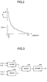
- Such a conventional apparatus uses a density-luminance conversion table which is not linear as shown in Fig. 2. Therefore, for example, a change in luminance level by one step at a low luminance level corresponds to M steps of the density level.
- noises are contained in a luminance signal read by a line sensor, the noises are emphasized at a low luminance level, i. e., at a high density level. Even if one step of the luminance level may produce a conspicuous white or black line on an output image.
- An image processing apparatus comprising a smoothing filter is for example described in EP-A-0216536 or EP-A-0 415 648.
- An embodiment of the present invention to provide an image processing apparatus capable of eliminating noises contained in image signals and improving an image resolution by performing an edge emphasis process of an area where a noise eliminating process is not applied.
- image processing apparatus as set out in claim 1.
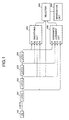
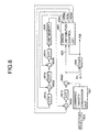
- Fig. 1 is a block diagram showing an image processing apparatus according to the first embodiment of the present invention.
- a contact sensor (CS) 100 photoelectrically converts an intensity signal of light reflected from an original into electrical signals, and outputs luminance data having six bits per pixel (64 tonal levels).
- Latches 201 to 204 constructed of D-type flip-flops receive the luminance data synchronously with pixel clocks, and output luminance data of four pixels in the main scan direction. Representing the luminance data outputted from the latch 202 as a subject pixel, outputted are the luminance data for the subject pixel, and the luminance data for preceding two pixels, and the luminance data for one succeeding pixel.
- a smoothing circuit 300 is constructed of adders 301 to 303 and a divider 304.
- the smoothing circuit 300 calculates a mean value of the luminance data for the four pixels in the main scan direction outputted from the latches 201 to 204, and outputs it to a selector 500.
- the adders 301 to 303 add together the data for the four pixels, and the divider 304 shifts the added data by two bits, i.e., the added data is divided by 4 to obtain a mean value.
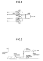
- the luminance judgment circuit 400 shown in Fig. 1 is constructed of comparators 401 to 404 and an AND gate 405 as shown in Fig. 4. If the four luminance data outputted from the latches 201 to 204 are all smaller than a value set to the comparators 401 to 404, a level "1" signal (truth) is outputted. In the other cases, a level "0" signal (falseness) is outputted.
- a selector 500 shown in Fig. 1 selects a smoothed data from the smoothing circuit if the luminance judgment circuit 400 outputs the level "1" signal, and selects the data (subject pixel data) from the latch 202 if the circuit 400 outputs the level "0" signal.
- the data selected by the selector 500 is outputted to a binarization circuit 600. Namely, if all the values of the luminance data for the subject pixel and peripheral three pixels are smaller than a predetermined value, the smoothed data is selected.
- the binarization circuit 600 performs luminance-density conversion shown in Fig. 2 for the data selected by the selector 500, and thereafter performs a pseudo half-tone process such as an error distribution method to output binarized image data.
- Fig. 8 shows an example of the structure of the binarization circuit shown in Fig. 1.
- a luminance-density conversion unit constructed of a ROM converts the luminance data into density data which is further converted into binarized data.
- Binarization may use a dither method, averaged error minimizing method, and the like.
- an error distribution method is used which binarizes density data by distributing binarization errors to peripheral pixels to obtain a variable magnification image having a good density conservation.
- 651a to 651d represent D-type flip-flops for latching data
- 652a to 652d represent adders
- 630 represents a line memory for one line delay
- 640 represents a comparator
- 660 represents an error distribution control circuit.
- image data of a multi-value (0 to 63) density outputted from a luminance-density conversion unit 601 is inputted to an adder 652d.
- the inputted multi-value density data original image multi-value data corresponding to subject pixel position (i, j)
- the comparator 640 compares the data on the signal line 650 with a predetermined threshold value TH (e.g., 32 for 6-bit data). If the data on the signal line 650 is larger than the threshold value TH, a level "1" signal (black) is outputted to a signal line 700, and if smaller, a level "0" signal (white) is outputted to the signal line 700.
- a predetermined threshold value TH e.g. 32 for 6-bit data
- the error distribution control circuit 660 If the output of the comparator 640 is "0" (white), the error distribution control circuit 660 outputs the data on the signal line 650. If the comparator 640 outputs "1" (black), the error distribution control circuit 660 calculates error quantities 656a to 656d distributed to the peripheral pixels using as an error a difference between the data on the signal line 650 and a constant T (63 for 6-bit data). The error quantity signals 656a to 656d are added at the adders 652a to 652d to the error quantities already distributed to the peripheral pixels (i - 1, j + 1), (i, j + 1), (i + 1, j + 1), and (i + 1, j), respectively of the subject pixel (i, j). The four peripheral pixels of the subject pixel are used in this embodiment. The number of pixels is not limited to this, but it may be increased or decreased as desired.
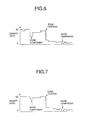
- a low luminance level where a change in luminance level by one bit is luminance-density converted into M bits change in density level, is greatly influenced by external noises contained in the luminance signal.
- the luminance signal shown in Fig. 5 is luminance-density converted into the density signal shown in Fig. 6.
- noises at a lower luminance level influence the density level more than noises at a higher luminance level.
- Eliminating noises only at a lower luminance level results in use of a noise eliminating filter only for a small image data distribution area. Therefore, as shown in Fig. 7, the edge portion is not influenced by averaging of noise elimination, and is not degraded.
- a combination of a noise elimination filter and a luminance judgment circuit allows noise elimination without deteriorating an image resolution.
- a mean value of peripheral four pixels is calculated.
- a mean value of n pixels in the main and sub scan directions may be used.
- a weighted filter such as a triangle filter may be used considering expected noise frequency components.
- a median filter for outputting a median value of reference pixel values may also be used in noise elimination.
- a noise eliminating filter operates when all reference pixel levels are lower than a predetermined luminance level, while considering a luminance-density conversion table.
- a noise eliminating filter may be used for a desired area in accordance with the characteristics of a conversion table.
- a filter is used only for an image area greatly influenced by noises. Therefore, noises can be effectively eliminated without deteriorating an image resolution.
- the second embodiment eliminates noises while performing an edge emphasis process for an area not using a noise eliminating filter, to thereby improve an image resolution.
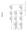
- Fig. 9 is a block diagram showing the main part of an image processing apparatus according to the second embodiment of the present invention.
- a contact sensor (CS) 1000 photoelectrically converts an intensity signal (luminance signal) of light reflected from an original into electrical signals.
- a sensor is not limited only to CS, but a line sensor of CCDs using optical reduction may also be used.
- An A/D converter 2000 converts an analog signal corrected by a shading correction circuit (not shown) and the like into digital luminance signal of six bits per pixel.
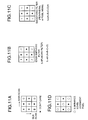
- a delay circuit 3000 is constructed of two FIFOs for two-line delay and five D-type flip-flops. Image data of two lines is delayed by the FIFOs to obtain image data of three lines at a time. The image data of three lines is inputted to the D-type flip-flops to delay it in the main scan direction. The D-type flip-flops obtain matrix image data A, B, C, D, and X shown in Fig. 11A which is then outputted to an calculation circuit at the following stage.
- a pixel X is used as a subject pixel to output a corrected value for X.
- a symbol “*" means "don't care” and is not used for calculation.
- An edge emphasis process circuit 4000 performs an edge emphasis filter (Laplacian filter) calculation process shown in Fig. 11B for the matrix pixel data A, B, C, D, and X supplied from the delay circuit 3000, and outputs resolution-compensated pixel data to a selector 7000.
- An edge emphasis filter calculation may use optional Laplacian filter values.
- a smoothing process circuit 5000 smoothes, as shown in Fig.
- the matric pixel data A, B, C, and D outputted from the delay circuit 3000 through calculation of a mean value thereof by using mean value calculating means, and outputs the smoothed pixel data (mean value of A, B, C, and D) to the selector 7000.
- a mean value of A, B, C, and D may be used for a smoothing filter.
- a luminance level judgment circuit 6000 outputs a level H (truth) signal when all the luminance values of the matrix pixel data A, B, C, D, X shown in Fig. 11D and obtained from the delay circuit 3000 are within a predetermined range, and in the other case outputs a level L (falseness) signal.
- a level H signal is outputted if the luminance value is equal to or higher than a present luminance value.
- the predetermined range is set as desired.
- the selector 7000 selects the image data from the smoothing process circuit 5000 when the level H signal is outputted from the luminance level judgment circuit 6000, and selects the image data from the edge emphasis process circuit 4000 when a level L signal is outputted.
- the image data from the selector 7000 with noises eliminated is converted into density data by LOG conversion described with Fig. 8 of the first embodiment.
- the density data is subject to a pseudo half-tone process such as an error distribution method, and is printed out from a binary value printer.
- the density data is subject to area modulation or the like to print it out.
- Fig. 10 shows the details of the delay circuit 3000.
- FIFO line buffers 2001 and 2002 delays the image data inputted from the A/D converter in the sub scan direction in units of line.
- One line is delayed by the FIFO line buffer 2001, and two lines are delayed by the FIFO line buffers 2001 and 2002.
- D-type flip-flops 2011 to 2018 delays the image data line-delayed by the FIFOs in the main scan direction in units of pixel, to thereby obtain the five matrix pixel data A, B, C, D, and X. Characters at upper right corners of the D-type flip-flops (D-FF) shown in Fig. 10 correspond to the pixel positions shown in Fig. 11A.
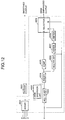
- Fig. 12 shows the details of the edge emphasis process circuit and smoothing circuit.
- An adder 4001 adds together the luminance signals for the peripheral pixels A, B, C, and D of the subject pixel.
- An output of the adder is used for both the smoothing process and edge emphasis process.
- a divider 5001 divides an output of the adder 4001 by 4 to obtain a mean value of the luminance signals. This division can be achieved by simply shifting two bits.
- a multiplier 4002 multiplies the luminance signal for the subject pixel by 4. This multiplication can be achieved by shifting two bits, similar to the case of the divider 5001.
- a sign inversion circuit 4003 inverts the sign of an output from the adder 4001 for the later subtraction.
- An adder 4004 adds together the outputs of the sign inversion circuit 4003 and the multiplier 4002.
- An output of the adder 4004 is a Laplacian filter value.
- a comparator 4005 determines whether the Laplacian filter value is within a predetermined range. If so, it supplies a selection signal to a selector 4009 to inhibit addition to the Laplacian value.
- a multiplier 4006 multiplies the Laplacian value to adjust the gain of the value.
- An adder 4007 adds the gain adjusted Laplacian value to the subject pixel value X.
- a limiter 4008 limits the data after addition of the Laplacian value to a minimum or maximum pixel value if the data is beyond the minimum or maximum pixel value.
- the selector 4009 selects the subject pixel value X if an output of the comparator 4005 indicates that the Laplacian value is within the predetermined range. In the other case, it selects the value after filtering.
- An output value of the selector 4009 becomes pixel data after the edge emphasis process.
- a block encircled by a broken line in Fig. 12 is a conventional edge emphasis circuit. In this embodiment, only the divider 5001 is added to provide the smoothing process.
- a low luminance level area is gieatly influenced by external noises contained in a luminance signal at the time of LOG conversion (luminance-density conversion), a change in luminance level by one bit resulting in a change in density level by n bits. Therefore, the smoothing filter is used only at the lower luminance level area to eliminate noise effects. On the contrary, noises at a higher luminance level have a tendency to be suppressed after LOG conversion, because of missing bits. It is therefore possible to effectively eliminate noises by performing the smoothing process only for an area having greater noise effects after LOG conversion (i.e., a smaller luminance level area).
- the smoothing filter is used only for the area having a small distribution of image data.
- the area including edge portions of an image is generally has a large data distribution. Accordingly, the smoothing process is not performed for this area. This can be easily achieved by limiting the luminance level of pixels.
- a combination of a smoothing filter and a luminance judgment circuit allows noise elimination without deteriorating an image resolution.
- a mean value of the matrix pixel data A, B, C, and D is calculated using the smoothing filter as shown in Fig. 11C. Therefore, it is possible to simplify the circuit by sharing the addition of A, B, C, and D with the calculation of 4X - (A + B + C + D) by the edge emphasis filter as shown in Fig. 11B. It is therefore unnecessary to add an adder for the smoothing process.
- the noise eliminating circuit of this embodiment can be realized by adding only the comparator for the luminance level judging circuit 6000 and the selector 7000, to a conventional edge emphasis circuit.
- the edge emphasis calculation and smoothing calculation have been performed using the peripheral pixels at the upper and lower, right and left positions of the subject pixel.
- An edge emphasis calculation may use peripheral pixels at right, left, upper, and lower positions of the subject pixel, and a smoothing calculation may use a mean value of the subject pixel and right and left peripheral pixels in the main scan direction.
- the embodiment uses a 3 x 3 matrix, other types of matrices may also be used.
- noise components superposed on a line sensor can be effectively suppressed with a small number of added circuits, while minimizing the deterioration of an image resolution.
Landscapes
- Engineering & Computer Science (AREA)
- Multimedia (AREA)
- Signal Processing (AREA)
- Facsimile Image Signal Circuits (AREA)
- Image Processing (AREA)
Claims (10)
- Appareil de traitement d'image comprenant:un moyen d'entrée (100) pour introduire des données d'image de luminance représentées par des pixels;un moyen (300) de traitement de lissage pour lisser les données d'image d'un pixel cible, en fonction des données d'image du pixel cible et de pixels prédéterminés périphériques audit pixel cible, reçues respectivement en provenance dudit moyen d'entrée; et caractérisé parun moyen de jugement (400) pour juger si le niveau des données de luminance dudit pixel cible et desdits pixels périphériques est ou non dans une plage prédéterminée; etun moyen (500) de commande de sortie pour délivrer sélectivement, soit les données d'image lissées par ledit moyen de traitement de lissage, soit les données d'image dudit pixel cible telles que reçues en provenance dudit moyen d'entrée, en fonction du résultat de jugement dudit moyen de jugement, le moyen de commande de sortie délivrant lesdites données d'image lissées lorsque ledit moyen de jugement juge que les données de luminance dudit pixel cible et desdits pixels périphériques sont dans ladite plage prédéterminée.
- Appareil selon la revendication 1, comprenant en outre un moyen de conversion (601) pour convertir lesdites données de luminance, en provenance dudit moyen de commande de sortie, en données de densité.
- Appareil selon la revendication 2, comprenant en outre un moyen (600) de mise sous forme binaire pour mettre lesdites données de densité en provenance dudit moyen de conversion sous forme binaire, par un procédé de répartition d'erreur.
- Appareil selon l'une quelconque des revendications précédentes, dans lequel ledit moyen de traitement de lissage délivre la valeur moyenne des données d'image dudit pixel cible et desdits pixels périphériques.
- Appareil selon l'une quelconque des revendications précédentes, comprenant en outre un moyen (4000) de traitement d'accentuation de bord pour exécuter un traitement d'accentuation de bord pour les données d'entrée du pixel cible, et dans lequel ledit moyen de commande de sortie délivre les données qui ont subi un traitement d'accentuation de bord si ledit moyen de jugement juge que les données de luminance du pixel cible et de ses pixels périphériques ne sont pas dans la plage prédéterminée.
- Procédé de traitement d'image comprenant les étapes suivantes:délivrance de données d'image de luminance se présentant sous la forme de pixels;lissage des données d'image d'un pixel cible reçues à partir de ladite étape d'introduction en fonction desdites données d'image du pixel cible et de pixels prédéterminés périphériques audit pixel cible;jugement du fait que le niveau desdites données d'image dudit pixel cible et desdits pixels périphériques est ou non dans une plage prédéterminée; etdélivrance sélective des données d'image lissées au cours de ladite étape de lissage, lorsqu'il est jugé que les données de luminance dudit pixel cible et des pixels périphériques sont dans ladite plage, et sinon, délivrance du pixel non lissé.
- Procédé selon la revendication 6, comprenant en outre une étape de conversion desdites données de luminance, obtenues au cours de ladite étape de commande de sortie, en données de densité.
- Procédé selon la revendication 7, comprenant en outre la mise sous forme binaire desdites données de densité obtenues au cours de ladite étape de conversion par un procédé de répartition d'erreur.
- Procédé selon l'une quelconque des revendications 6, 7 et 8, dans lequel ladite étape de traitement de lissage délivre une valeur moyenne des données d'image dudit pixel cible et desdits pixels périphériques.
- Procédé selon l'une quelconque des revendications 6 à 9, comprenant en outre une étape d'exécution d'un traitement d'accentuation de bord pour les données d'entrée du pixel cible, et dans lequel, au cours de ladite étape de commande de sortie, les données qui ont subi un traitement d'accentuation de bord sont délivrées s'il est jugé au cours de ladite étape de jugement que les données de luminance du pixel cible et de ses pixels périphériques ne sont pas dans la plage prédéterminée.
Applications Claiming Priority (2)
| Application Number | Priority Date | Filing Date | Title |
|---|---|---|---|
| JP8763491 | 1991-03-27 | ||
| JP87634/91 | 1991-03-27 |
Publications (3)
| Publication Number | Publication Date |
|---|---|
| EP0506380A2 EP0506380A2 (fr) | 1992-09-30 |
| EP0506380A3 EP0506380A3 (fr) | 1992-11-04 |
| EP0506380B1 true EP0506380B1 (fr) | 1996-07-17 |
Family
ID=13920411
Family Applications (1)
| Application Number | Title | Priority Date | Filing Date |
|---|---|---|---|
| EP92302597A Expired - Lifetime EP0506380B1 (fr) | 1991-03-27 | 1992-03-26 | Appareil de traitement d'images |
Country Status (5)
| Country | Link |
|---|---|
| US (1) | US5539541A (fr) |
| EP (1) | EP0506380B1 (fr) |
| CN (1) | CN1023918C (fr) |
| DE (1) | DE69212192T2 (fr) |
| ES (1) | ES2089393T3 (fr) |
Families Citing this family (14)
| Publication number | Priority date | Publication date | Assignee | Title |
|---|---|---|---|---|
| JP3489796B2 (ja) * | 1994-01-14 | 2004-01-26 | 株式会社リコー | 画像信号処理装置 |
| JPH09261481A (ja) * | 1996-03-22 | 1997-10-03 | Toshiba Corp | 画像形成装置 |
| US5778156A (en) * | 1996-05-08 | 1998-07-07 | Xerox Corporation | Method and system for implementing fuzzy image processing of image data |
| JP2000138833A (ja) | 1998-08-28 | 2000-05-16 | Toshiba Tec Corp | 画像処理方法及び画像処理装置 |
| US6674915B1 (en) * | 1999-10-07 | 2004-01-06 | Sony Corporation | Descriptors adjustment when using steerable pyramid to extract features for content based search |
| US6621595B1 (en) * | 2000-11-01 | 2003-09-16 | Hewlett-Packard Development Company, L.P. | System and method for enhancing scanned document images for color printing |
| DE10208290C1 (de) | 2002-02-26 | 2003-07-24 | Koenig & Bauer Ag | Verfahren zur Signalauswertung eines elektronischen Bildsensors |
| JP4135737B2 (ja) * | 2005-08-30 | 2008-08-20 | ブラザー工業株式会社 | 画像処理プログラム |
| KR101303660B1 (ko) | 2007-10-01 | 2013-09-04 | 삼성전자주식회사 | 잡음제거를 고려한 선명도 향상 방법 및 장치 그리고 잡음가중치 계산 방법 및 장치 |
| JP4933418B2 (ja) * | 2007-12-21 | 2012-05-16 | キヤノン株式会社 | 画像読取装置、マルチファンクションプリンタ装置、及び画像処理方法 |
| US8243351B2 (en) * | 2007-12-21 | 2012-08-14 | Canon Kabushiki Kaisha | Image reading apparatus, multifunction printer apparatus, and image processing method |
| JP4989444B2 (ja) * | 2007-12-21 | 2012-08-01 | キヤノン株式会社 | 画像読取装置、マルチファンクションプリンタ装置、及び画像処理方法 |
| JP6303816B2 (ja) * | 2014-05-28 | 2018-04-04 | 富士ゼロックス株式会社 | 画像処理装置及びプログラム |
| US11423515B2 (en) * | 2019-11-06 | 2022-08-23 | Canon Kabushiki Kaisha | Image processing apparatus |
Family Cites Families (6)
| Publication number | Priority date | Publication date | Assignee | Title |
|---|---|---|---|---|
| JPS60253368A (ja) * | 1983-11-10 | 1985-12-14 | Dainippon Screen Mfg Co Ltd | 複製画像記録表示等に於けるjag除去方法 |
| EP0212990B1 (fr) * | 1985-08-29 | 1992-10-28 | Canon Kabushiki Kaisha | Appareil de traitement d'images |
| JP2589298B2 (ja) * | 1987-01-28 | 1997-03-12 | キヤノン株式会社 | 符号化画像データの復号化装置 |
| JPH02250464A (ja) * | 1989-03-24 | 1990-10-08 | Sharp Corp | ファクシミリ装置 |
| DE69032318T2 (de) * | 1989-08-31 | 1998-09-24 | Canon Kk | Vorrichtung zur Bildverarbeitung |
| US5818489A (en) * | 1994-12-07 | 1998-10-06 | Canon Kabushiki Kaisha | Image forming apparatus and process cartridge having exposure device using light beam having specific spot area |
-
1992
- 1992-03-26 ES ES92302597T patent/ES2089393T3/es not_active Expired - Lifetime
- 1992-03-26 EP EP92302597A patent/EP0506380B1/fr not_active Expired - Lifetime
- 1992-03-26 DE DE69212192T patent/DE69212192T2/de not_active Expired - Lifetime
- 1992-03-27 CN CN92102968.3A patent/CN1023918C/zh not_active Expired - Lifetime
-
1994
- 1994-11-03 US US08/334,352 patent/US5539541A/en not_active Expired - Lifetime
Also Published As
| Publication number | Publication date |
|---|---|
| US5539541A (en) | 1996-07-23 |
| ES2089393T3 (es) | 1996-10-01 |
| CN1066137A (zh) | 1992-11-11 |
| DE69212192D1 (de) | 1996-08-22 |
| EP0506380A2 (fr) | 1992-09-30 |
| DE69212192T2 (de) | 1996-12-05 |
| EP0506380A3 (fr) | 1992-11-04 |
| CN1023918C (zh) | 1994-03-02 |
Similar Documents
| Publication | Publication Date | Title |
|---|---|---|
| US5068746A (en) | Image processing apparatus | |
| EP0506380B1 (fr) | Appareil de traitement d'images | |
| US5886797A (en) | Method and apparatus for controlling a spatial filtering process based on characteristics of image data | |
| US5157741A (en) | Image processing method and apparatus for out-putting dot-processed data with suppression of false contours and other noise | |
| US5570461A (en) | Image processing using information of one frame in binarizing a succeeding frame | |
| US5488672A (en) | Color image processing apparatus | |
| EP0814600B1 (fr) | Procédé et système pour le traitement de données d'images | |
| EP0575995B1 (fr) | Dispositif de réduction de bruit | |
| JP3165225B2 (ja) | 画像処理装置および画像処理方法 | |
| JP2927155B2 (ja) | 画像処理装置 | |
| JPS62242473A (ja) | 疑似中間調画像処理装置 | |
| JPH0738767A (ja) | 画像2値化処理装置 | |
| JP3245600B2 (ja) | 画像処理装置 | |
| JPH01115271A (ja) | 画像処理装置 | |
| JPH06284291A (ja) | 画像処理装置 | |
| JPH07302190A (ja) | 除算器並びにこれを用いた画像信号読取装置 | |
| JPH0668250A (ja) | 画像処理装置 | |
| JPH0145273B2 (fr) | ||
| JPS63288567A (ja) | 画像処理装置 | |
| JPH065879B2 (ja) | 画像処理装置 | |
| JP3157870B2 (ja) | 画像処理方式 | |
| JP2558915B2 (ja) | 黒判定装置及び領域識別装置 | |
| JPS61157163A (ja) | 画像処理装置 | |
| JPH07135584A (ja) | 映像信号処理装置 | |
| JPS61157162A (ja) | 画像処理装置 |
Legal Events
| Date | Code | Title | Description |
|---|---|---|---|
| PUAI | Public reference made under article 153(3) epc to a published international application that has entered the european phase |
Free format text: ORIGINAL CODE: 0009012 |
|
| PUAL | Search report despatched |
Free format text: ORIGINAL CODE: 0009013 |
|
| AK | Designated contracting states |
Kind code of ref document: A2 Designated state(s): DE ES FR GB IT |
|
| AK | Designated contracting states |
Kind code of ref document: A3 Designated state(s): DE ES FR GB IT |
|
| 17P | Request for examination filed |
Effective date: 19930319 |
|
| 17Q | First examination report despatched |
Effective date: 19950215 |
|
| GRAH | Despatch of communication of intention to grant a patent |
Free format text: ORIGINAL CODE: EPIDOS IGRA |
|
| GRAA | (expected) grant |
Free format text: ORIGINAL CODE: 0009210 |
|
| AK | Designated contracting states |
Kind code of ref document: B1 Designated state(s): DE ES FR GB IT |
|
| GRAH | Despatch of communication of intention to grant a patent |
Free format text: ORIGINAL CODE: EPIDOS IGRA |
|
| REF | Corresponds to: |
Ref document number: 69212192 Country of ref document: DE Date of ref document: 19960822 |
|
| ET | Fr: translation filed | ||
| REG | Reference to a national code |
Ref country code: ES Ref legal event code: FG2A Ref document number: 2089393 Country of ref document: ES Kind code of ref document: T3 |
|
| ITF | It: translation for a ep patent filed | ||
| REG | Reference to a national code |
Ref country code: ES Ref legal event code: FG2A Ref document number: 2089393 Country of ref document: ES Kind code of ref document: T3 |
|
| PLBE | No opposition filed within time limit |
Free format text: ORIGINAL CODE: 0009261 |
|
| STAA | Information on the status of an ep patent application or granted ep patent |
Free format text: STATUS: NO OPPOSITION FILED WITHIN TIME LIMIT |
|
| 26N | No opposition filed | ||
| REG | Reference to a national code |
Ref country code: GB Ref legal event code: IF02 |
|
| PGFP | Annual fee paid to national office [announced via postgrant information from national office to epo] |
Ref country code: ES Payment date: 20100225 Year of fee payment: 19 |
|
| PGFP | Annual fee paid to national office [announced via postgrant information from national office to epo] |
Ref country code: GB Payment date: 20100309 Year of fee payment: 19 |
|
| PGFP | Annual fee paid to national office [announced via postgrant information from national office to epo] |
Ref country code: FR Payment date: 20100414 Year of fee payment: 19 |
|
| PGFP | Annual fee paid to national office [announced via postgrant information from national office to epo] |
Ref country code: IT Payment date: 20100329 Year of fee payment: 19 |
|
| PGFP | Annual fee paid to national office [announced via postgrant information from national office to epo] |
Ref country code: DE Payment date: 20110331 Year of fee payment: 20 |
|
| GBPC | Gb: european patent ceased through non-payment of renewal fee |
Effective date: 20110326 |
|
| REG | Reference to a national code |
Ref country code: FR Ref legal event code: ST Effective date: 20111130 |
|
| PG25 | Lapsed in a contracting state [announced via postgrant information from national office to epo] |
Ref country code: FR Free format text: LAPSE BECAUSE OF NON-PAYMENT OF DUE FEES Effective date: 20110331 |
|
| PG25 | Lapsed in a contracting state [announced via postgrant information from national office to epo] |
Ref country code: GB Free format text: LAPSE BECAUSE OF NON-PAYMENT OF DUE FEES Effective date: 20110326 Ref country code: IT Free format text: LAPSE BECAUSE OF NON-PAYMENT OF DUE FEES Effective date: 20110326 |
|
| REG | Reference to a national code |
Ref country code: DE Ref legal event code: R071 Ref document number: 69212192 Country of ref document: DE |
|
| REG | Reference to a national code |
Ref country code: DE Ref legal event code: R071 Ref document number: 69212192 Country of ref document: DE |
|
| REG | Reference to a national code |
Ref country code: ES Ref legal event code: FD2A Effective date: 20120423 |
|
| PG25 | Lapsed in a contracting state [announced via postgrant information from national office to epo] |
Ref country code: DE Free format text: LAPSE BECAUSE OF EXPIRATION OF PROTECTION Effective date: 20120327 |
|
| PG25 | Lapsed in a contracting state [announced via postgrant information from national office to epo] |
Ref country code: ES Free format text: LAPSE BECAUSE OF NON-PAYMENT OF DUE FEES Effective date: 20110327 |