EP0505751B1 - Circuit amplificateur logarithmique - Google Patents
Circuit amplificateur logarithmique Download PDFInfo
- Publication number
- EP0505751B1 EP0505751B1 EP92103178A EP92103178A EP0505751B1 EP 0505751 B1 EP0505751 B1 EP 0505751B1 EP 92103178 A EP92103178 A EP 92103178A EP 92103178 A EP92103178 A EP 92103178A EP 0505751 B1 EP0505751 B1 EP 0505751B1
- Authority
- EP
- European Patent Office
- Prior art keywords
- transistors
- full
- emitter resistor
- differential
- wave rectifiers
- Prior art date
- Legal status (The legal status is an assumption and is not a legal conclusion. Google has not performed a legal analysis and makes no representation as to the accuracy of the status listed.)
- Expired - Lifetime
Links
Images


Classifications
-
- H—ELECTRICITY
- H03—ELECTRONIC CIRCUITRY
- H03G—CONTROL OF AMPLIFICATION
- H03G7/00—Volume compression or expansion in amplifiers
- H03G7/001—Volume compression or expansion in amplifiers without controlling loop
-
- H—ELECTRICITY
- H03—ELECTRONIC CIRCUITRY
- H03G—CONTROL OF AMPLIFICATION
- H03G7/00—Volume compression or expansion in amplifiers
- H03G7/06—Volume compression or expansion in amplifiers having semiconductor devices
Definitions
- This invention relates to a logarithmic amplification circuit.
- a logarithmic amplification circuit shown in Fig. 1 is well-known as a conventional one, which is a logarithmic amplification circuit described in the Plessey Corporation's Catalogue SL521, and comprises a differential amplifier consisting of transistors TR1 and TR2 as a first stage and a half-wave rectifier consisting of a differential transistor pair TR4 and TR5 only one transistor of which has an emitter resistor RE (the emitter resistor RE is connected to the transistor TR5 in Fig. 1) as a second stage.
- the operational principle thereof will be explained below.
- a voltage to be applied between the transistors TR4 and TR5 is expressed as VB4.5.
- base voltages of the transistors TR4 and TR5 are respectively expressed as VBE4 and VBE5.
- the maximum absolute value may satisfy the following equation
- Fig. 2 shows a relation of a voltage between the bases VB4,5 and the collector current Ic5.
- the inter-base voltage VB4,5 is required to be provided with a voltage offset of about 4VT (about 100 mV). Therefore, the conventional logarithmic amplification circuit is unavoidably necessary to have a circuit for providing a voltage offset to the differential input voltage (VB4,5), which means that there exists such a problem that not only the input circuit is complicated, but also the dynamic range is difficult to be expanded.
- it utilizes the half - wave rectification characteristic, resulting in arising a problem that amplification is difficult to be carried out with high accuracy.
- EP-A-0 248 428 discloses a bipolar logarithmic amplifier having half-or full-wave rectifiers consisting of unbalanced emitter-coupled transistor pairs whose emitter areas are different from each other.
- the emitter area difference adds an input offset voltage to the emitter-coupled pair. Therefore, the emitter-coupled pair whose emitter area ratio is K (K > 1) is a half-wave rectifier.
- the cross-coupled, emitter-coupled transistor pair whose emitter area ratio is K operates as a full-wave rectifier. To make the rectification characteristic of the rectifier different from each other, a very large value of K and an emitter resistor are required.
- US-A-4 990 803 discloses a similar bipolar logarithmic amplifier. The difference between the two amplifiers is that an input offset voltage is produced outside the transistor pair in EP-A-0 248 428, and that the input offset voltage is produced within the transistor pair in the amplifier of US-A-4 990 803.
- JP-A-2-265310 discloses a logarithmic compression amplifier with cascade-connected half-wave rectifiers and an adder without any differential amplifier and which has a pseudo - logarithmic half-wave rectifier characteristic.
- EP-A-0 484 139 discloses a logarithmic amplifying circuit, and it is cited here because it falls under Art. 54(3) EPC.
- an object of this invention is to provide a logarithmic amplification circuit which has a simple input circuit and a wide dynamic range as compared with conventional ones.
- Another object of this invention is to provide a logarithmic amplification circuit capable of performing high accuracy amplification.
- a logarithmic full-wave rectifier is used as the full-wave rectifier.
- the logarithmic full - wave rectifier comprises two sets of differential transistor pair only one transistor of which has an emitter resistor.
- a plurality of logarithmic full-wave rectifiers as shown above are provided so as to be different in the product of a resistance value of the emitter resistor and a current value of the constant current source from each other and connected in series to each other.
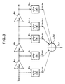
- Fig. 3 schematically shows a logarithmic amplification circuit according to one embodiment of this invention.
- the logarithmic amplification circuit shown in Fig. 3 comprises n differential amplifiers A1 to An (gains GV1 to GVn) connected in series, (n+1) full-wave rectifiers B0 to Bn respectively receiving input signals to or output signals from the differential amplifiers A1 to An for rectification, and an adder ADD for adding the output currents IOUT0 to IOUTn from the (n+1) full-wave rectifiers B0 to Bn.
- the rectifier B0 receives an input signal to be inputted to the differential amplifier A1, the rectifiers B1 to Bn receive output signals outputted from the differential amplifiers A1 to An, respectively.
- the adder ADD adds the outputs IOUT0 through IOUTn outputted respectively from the (n+1) rectifiers B0 to Bn and outputs an output current IOUT.
- the full-wave rectifiers B0 to Bn each is arranged as shown in Fig. 4.
- transistors Q1 and Q2 form a first differential transistor pair whose emitters are connected with each other through an emitter resistor
- transistors Q3 and Q4 form a second differential transistor pair whose emitters are connected with each other through an emitter resistor.
- each ofthe transistors Q2 and Q3 only has an emitter resistor.
- the collectors of the transistors Q2 and Q3 each having an emitter resistor are connected with each other, while the collectors of the transistors Q1 and Q4 each not having an emitter resistor are also connected with each other.
- the bases of the transistor Q1 not having an emitter resistor and the transistor Q3 having an emitter resistor and the bases of the transistor Q2 having an emitter resistor and the transistor Q4 not having an emitter resistor are connected with each other, respectively, and a differential input voltage Vi which is an input signal to or an output signal from said differential amplifier is applied between the common bases.
- the differential transistor pairs Q1, Q2 and Q3, Q4 are connected respectively to constant current sources I0.
- this full-wave rectifier includes two differential transistor pairs, wherein only one of the transistors of each pair has an emitter resistor, the differential transistor pair each has the same structure as the circuit shown in Fig.1, and their inputs are connected inversely to each other. Namely, these are arranged so that an input signal of the second differential transistor pair Q3 and Q4 is made inverse in phase to an input signal of the first differential transistor pair Q1 and Q2. As a result, respective collector currents Ic1, Ic2, Ic3, and Ic4 of the transistors Q1, Q2, Q3 and Q4 are varied equally to those shown in Fig. 2 (see Fig. 5).
- Fig. 7 shows another arrangement of the (n+1) full-wave rectifiers B0 to Bn shown in Fig. 3.
- the circuit shown in Fig. 7 is a pseudo logarithmic full-wave rectifier including a plurality of full-wave rectifiers shown in Fig. 4 connected in parallel, which respectively have emitter resistor having different resistance values RE, RE', RE'', ⁇ from each other, and constant current sources having different current values I0, I0', I0'', ## from each other.
- emitter resistor having different resistance values RE, RE', RE'', ⁇ from each other
- constant current sources having different current values I0, I0', I0'', ## from each other.
- a first full-wave rectifier including a differential transistor pair Q1 and Q2 and a differential transistor pair Q3 and Q4, a second full-wave rectifier including a differential transistor pair Q1' and Q2' and a differential transistor pair Q3' and Q4', and a third full-wave rectifier including a differential transistor pair Q1'' and Q2'' and a differential transistor pair Q3'' and Q4' are shown.
- the input voltage Vi is applied between the common bases of each full - wave rectifier, that is, in the first rectifier, it is applied between the common base of the transistors Q1 and Q3 and the common base of the transistors Q2 and Q4, in the second rectifier, it is applied between the common base of the transistors Q1' and Q3' and the common base of the transistors Q2' and Q4', and in the third rectifier, it is applied between the common base of the transistors Q1'' and Q3'' and the common base of the transistors Q2'' and Q4''.
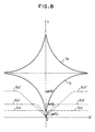
- the output currents I3 and I4 are logarithmic in characteristic and can be approximated by the dotted lines in the negative range and the positive range of the input voltage Vi, respectively (see Fig. 8).
- the change of I7 becomes as shown in Fig. 8.
- the circuit shown in Fig. 7 has a logarithmic full-wave rectification characteristic.
- this rectification characteristic has the positive range and negative range of Vi symmetrical with respect to each other.
- the I7 can be approximated to the logarithmic full - wave rectification characteristic even when the condition shown by Eq. (14) is not existing.
- the output currents I7 and I8 are inverse in phase to each other, so that the output current I8 also can be approximated to a logarithmic characteristic similar to the case shown above.
- the circuit shown in Fig. 7 has a logarithmic full-wave rectification characteristic as shown in Fig. 8.
- the n differential amplifiers A1, A2, ⁇ , and An connected in series shown in Fig. 3 have the gains [dB] GV1, GV2, ⁇ , and GVn. respectively, however, if a signal having a large amplitude is inputted, the output is saturated, resulting in effecting a limiting operation.
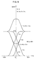
- the full-wave rectifier as shown in Fig. 4 as each of the rectifiers B0, B1, ⁇ and Bn and adding the respective outputs IOUT0 to IOUTn to each other through the adder ADD, the output current IOUT thereof has a logarithmic amplification characteristic as shown in Fig. 9.
- the circuit shown in Fig. 3 is a logarithmic amplification circuit.
- This logarithmic amplification circuit can eliminate a voltage offset, so that an input circuit can be made simple, and yet the dynamic range can be widened by lowering the lower limit thereof.
- each of the rectifiers B0, B1, ⁇ , and Bn uses two sets of differential transistor pair, so that a dispersion in characteristic of components can be set off to each other, being possible to effect high accuracy amplification.
- the logarithmic amplification characteristic of the output current IOUT of the logarithmic amplification circuit of this invention can be improved by appropriately selecting each of the gains GV1, GV2, ⁇ , and GVn of respective differential amplifiers A1, A2, ⁇ , and An, and the current value of the constant current source I0, the resistance value of the emitter resistor RE and the current amplification factor ⁇ F of each of the full-wave rectifiers B0, B1, ⁇ , and Bn. For example, by lowering the gains GV1, GV2, ⁇ , and GVn of respective differential amplifiers A1, A2, ⁇ , and An, the logarithmic characteristic can be improved. On the other hand, however, this disadvantageously results in a decrease in dynamic range of the output.
- the dynamic range of the full-wave rectifier shown in Fig. 4 is only at a level of about 10 dB as shown in Fig. 6, so that the logarithmic output IOUT becomes irregular, resulting in being inferior in linearity.
- the dynamic range can be expanded while improving the logarithmic characteristic. Therefore, even if the number of stages of the differential amplifiers to be used is reduced, a high accuracy logarithmic amplification circuit with a wide dynamic range can be realized.
Landscapes
- Tone Control, Compression And Expansion, Limiting Amplitude (AREA)
- Amplifiers (AREA)
Claims (6)
- Circuit d'amplification logarithmique bipolaire comprenant:un amplificateur différentiel (A1 à An);au moins deux redresseurs pleines ondes (B0 à Bn) englobant chacun deux redresseurs demi-ondes (Q1, Q2; Q3, Q4, respectivement) reliés de telle sorte que leurs signaux d'entrée se trouvent en inversion de phase l'un par rapport à l'autre et dans lesquels les redresseurs pleines ondes reçoivent un signal d'entrée et un signal de sortie dudit amplificateur différentiel, respectivement; etun additionneur (ADD) pour additionner les signaux de sortie desdits redresseurs pleines ondes;dans lequel chacun desdits redresseurs demi-ondes englobe une paire de transistors différentiels couplés à un émetteur asymétrique et un seul transistor de chacune desdites paires de transistors possède une résistance d'émetteur (RE).
- Circuit selon la revendication 1, dans lequel lesdits deux jeux de paires de transistors différentiels sont arrangés de telle sorte que les collecteurs des transistors possédant respectivement une résistance d'émetteur sont reliés l'un à l'autre, les collecteurs des transistors ne possédant pas respectivement une résistance d'émetteur sont reliés l'un à l'autre, un signal parmi le signal de sortie et le signal d'entrée dudit amplificateur différentiel est appliqué à la base d'un des transistors possédant respectivement une résistance d'émetteur et d'un des transistors ne possédant pas respectivement une résistance d'émetteur, l'autre signal parmi le signal de sortie et le signal d'entrée dudit amplificateur différentiel est appliqué à la base de l'autre transistor possédant respectivement une résistance d'émetteur et de l'autre transistor ne possédant pas respectivement une résistance d'émetteur, et les transistors de chaque paire sont reliés à une source de courant constant d'une manière respective.
- Circuit d'amplification logarithmique comprenant:n amplificateurs différentiels (A1 à An), n représentant un entier égal à deux ou plus, montés en série l'un à l'autre;(n+1) redresseurs pleines ondes (B0 à Bn) englobant chacun deux redresseurs demi-ondes dont les signaux d'entrée se trouvent en inversion de phase l'un par rapport à l'autre, dans lesquels le premier desdits (n+1) redresseurs pleines ondes reçoit un signal d'entrée vers le premier desdits n amplificateurs différentiels et les autres redresseurs pleines ondes reçoiventdes signaux de sortie desdits n amplificateurs différentiels, d'une manière respective ; etun additionneur (ADD) pour additionner les signaux de sortie desdits (n+1) redresseurs pleines ondes;dans lequel chacun desdits redresseurs demi-ondes englobe une paire de transistors différentiels couplés à un émetteur asymétrique et un seul transistor de chacune desdites paires de transistors possède une résistance d'émetteur (RE).
- Circuit selon la revendication 3, dans lequel lesdits deux jeux de paires de transistors différentiels sont arrangés de telle sorte que les collecteurs des transistors possédant respectivement une résistance d'émetteur sont reliés l'un à l'autre, les collecteurs des transistors ne possédant pas respectivement une résistance d'émetteur sont reliés l'un à l'autre, un signal parmi le signal de sortie et le signal d'entrée de chacun desdits n amplificateurs différentiels est appliqué à la base d'un des transistors possédant respectivement une résistance d'émetteur et d'un des transistors ne possédant pas respectivement une résistance d'émetteur, l'autre signal parmi le signal de sortie et le signal d'entrée de chacun desdits n amplificateurs différentiels est appliqué à la base de l'autre transistor possédant respectivement une résistance d'émetteur et de l'autre transistor ne possédant pas respectivement une résistance d'émetteur, et les transistors de chaque paire sont reliés à des sources de courant constant d'une manière respective.
- Circuit selon l'une quelconque des revendications 1 à 4, dans lequel lesdits redresseurs pleines ondes comprennent un redresseur pleine onde logarithmique.
- Circuit selon la revendication 5, dans lequel ledit redresseur pleine onde logarithmique comprend plusieurs redresseurs pleines ondes englobant chacun deux jeux de paires de transistors différentiels, dont seulement un transistor possède une résistance d'émetteur, et des sources de courant constant pour alimenter en courant électrique lesdits deux jeux de paires de transistors différentiels d'une manière respective, dans lequel lesdits plusieurs redresseurs pleines ondes sont différents les uns des autres en ce qui concerne le produit de la valeur de résistance de ladite résistance d'émetteur et de la valeur de courant de chacune desdites sources de courant constant et sont montés en parallèle l'un à l'autre.
Applications Claiming Priority (3)
| Application Number | Priority Date | Filing Date | Title |
|---|---|---|---|
| JP3057918A JP2995886B2 (ja) | 1991-02-28 | 1991-02-28 | 対数増幅回路 |
| JP57918/91 | 1991-02-28 | ||
| JP5791891 | 1991-02-28 |
Publications (3)
| Publication Number | Publication Date |
|---|---|
| EP0505751A2 EP0505751A2 (fr) | 1992-09-30 |
| EP0505751A3 EP0505751A3 (en) | 1993-03-17 |
| EP0505751B1 true EP0505751B1 (fr) | 2001-11-07 |
Family
ID=13069380
Family Applications (1)
| Application Number | Title | Priority Date | Filing Date |
|---|---|---|---|
| EP92103178A Expired - Lifetime EP0505751B1 (fr) | 1991-02-28 | 1992-02-25 | Circuit amplificateur logarithmique |
Country Status (7)
| Country | Link |
|---|---|
| US (1) | US5561392A (fr) |
| EP (1) | EP0505751B1 (fr) |
| JP (1) | JP2995886B2 (fr) |
| AU (1) | AU651432B2 (fr) |
| CA (1) | CA2062010C (fr) |
| DE (1) | DE69232182T2 (fr) |
| ES (1) | ES2162790T3 (fr) |
Families Citing this family (18)
| Publication number | Priority date | Publication date | Assignee | Title |
|---|---|---|---|---|
| EP0514929B1 (fr) * | 1991-05-23 | 1999-09-22 | Nec Corporation | Amplificateur logarithmique IF |
| JP2836452B2 (ja) * | 1993-07-14 | 1998-12-14 | 日本電気株式会社 | 対数増幅回路 |
| US5489868A (en) * | 1994-10-04 | 1996-02-06 | Analog Devices, Inc. | Detector cell for logarithmic amplifiers |
| JPH08330861A (ja) * | 1995-05-31 | 1996-12-13 | Nec Corp | 低電圧オペレーショナルトランスコンダクタンスアンプ |
| JP2778537B2 (ja) * | 1995-07-14 | 1998-07-23 | 日本電気株式会社 | Agcアンプ |
| US5815039A (en) * | 1995-07-21 | 1998-09-29 | Nec Corporation | Low-voltage bipolar OTA having a linearity in transconductance over a wide input voltage range |
| AU6572296A (en) * | 1995-09-19 | 1997-03-27 | Nec Corporation | Bipolar operational transconductance amplifier |
| JP2874616B2 (ja) * | 1995-10-13 | 1999-03-24 | 日本電気株式会社 | Ota及びマルチプライヤ |
| JPH09219630A (ja) * | 1995-12-08 | 1997-08-19 | Nec Corp | 差動回路 |
| JPH09238032A (ja) * | 1996-02-29 | 1997-09-09 | Nec Corp | Otaおよびバイポーラマルチプライヤ |
| DE19608861A1 (de) * | 1996-03-07 | 1997-09-11 | Philips Patentverwaltung | Schaltungsanordnung mit einer logarithmischen Übertragungsfunktion |
| US5920215A (en) * | 1997-06-30 | 1999-07-06 | Sun Microsystems, Inc. | Time-to-charge converter circuit |
| US6166592A (en) * | 1998-07-31 | 2000-12-26 | Lucent Technologies Inc. | Linear CMOS transconductor with rail-to-rail compliance |
| US5994959A (en) * | 1998-12-18 | 1999-11-30 | Maxim Integrated Products, Inc. | Linearized amplifier core |
| US20050057298A1 (en) * | 2003-09-16 | 2005-03-17 | Kevin Gamble | Demodulating logarithmic amplifier and method of amplification |
| US7002395B2 (en) * | 2003-09-16 | 2006-02-21 | Yuantonix, Inc. | Demodulating logarithmic amplifier |
| US7417485B1 (en) | 2003-09-23 | 2008-08-26 | Cypress Semiconductor Corporation | Differential energy difference integrator |
| EP2713507B1 (fr) | 2012-10-01 | 2014-12-10 | Nxp B.V. | Détecteur de puissance RF utilisant FET |
Citations (2)
| Publication number | Priority date | Publication date | Assignee | Title |
|---|---|---|---|---|
| US4990803A (en) * | 1989-03-27 | 1991-02-05 | Analog Devices, Inc. | Logarithmic amplifier |
| EP0484139A1 (fr) * | 1990-10-30 | 1992-05-06 | Nec Corporation | Circuit amplificateur logarithmique |
Family Cites Families (9)
| Publication number | Priority date | Publication date | Assignee | Title |
|---|---|---|---|---|
| US4794342A (en) * | 1986-06-04 | 1988-12-27 | Nec Corporation | Intermediate frequency amplification circuit capable of detecting a field strength with low electric power |
| JPH0622304B2 (ja) * | 1986-06-12 | 1994-03-23 | 日本電気株式会社 | 対数if増幅回路 |
| DE68912363T2 (de) * | 1988-02-29 | 1994-07-28 | Philips Nv | Logarithmischer Verstärker. |
| NL8800510A (nl) * | 1988-02-29 | 1989-09-18 | Philips Nv | Schakeling voor het lineair versterken en demoduleren van een am-gemoduleerd signaal en geintegreerd halfgeleiderelement daarvoor. |
| JPH02265310A (ja) * | 1989-04-05 | 1990-10-30 | Nec Corp | 対数圧縮増幅回路 |
| JP2643516B2 (ja) * | 1990-02-01 | 1997-08-20 | 日本電気株式会社 | 対数増幅回路 |
| US5070303A (en) * | 1990-08-21 | 1991-12-03 | Telefonaktiebolaget L M Ericsson | Logarithmic amplifier/detector delay compensation |
| US5319267A (en) * | 1991-01-24 | 1994-06-07 | Nec Corporation | Frequency doubling and mixing circuit |
| US5298811A (en) * | 1992-08-03 | 1994-03-29 | Analog Devices, Inc. | Synchronous logarithmic amplifier |
-
1991
- 1991-02-28 JP JP3057918A patent/JP2995886B2/ja not_active Expired - Fee Related
-
1992
- 1992-02-25 EP EP92103178A patent/EP0505751B1/fr not_active Expired - Lifetime
- 1992-02-25 DE DE69232182T patent/DE69232182T2/de not_active Expired - Fee Related
- 1992-02-25 ES ES92103178T patent/ES2162790T3/es not_active Expired - Lifetime
- 1992-02-26 AU AU11258/92A patent/AU651432B2/en not_active Ceased
- 1992-02-27 CA CA002062010A patent/CA2062010C/fr not_active Expired - Fee Related
-
1993
- 1993-08-05 US US08/102,493 patent/US5561392A/en not_active Expired - Fee Related
Patent Citations (2)
| Publication number | Priority date | Publication date | Assignee | Title |
|---|---|---|---|---|
| US4990803A (en) * | 1989-03-27 | 1991-02-05 | Analog Devices, Inc. | Logarithmic amplifier |
| EP0484139A1 (fr) * | 1990-10-30 | 1992-05-06 | Nec Corporation | Circuit amplificateur logarithmique |
Also Published As
| Publication number | Publication date |
|---|---|
| US5561392A (en) | 1996-10-01 |
| EP0505751A3 (en) | 1993-03-17 |
| JPH04273708A (ja) | 1992-09-29 |
| CA2062010A1 (fr) | 1992-08-29 |
| AU1125892A (en) | 1992-09-03 |
| JP2995886B2 (ja) | 1999-12-27 |
| ES2162790T3 (es) | 2002-01-16 |
| DE69232182T2 (de) | 2002-04-11 |
| EP0505751A2 (fr) | 1992-09-30 |
| AU651432B2 (en) | 1994-07-21 |
| CA2062010C (fr) | 1997-04-22 |
| DE69232182D1 (de) | 2001-12-13 |
Similar Documents
| Publication | Publication Date | Title |
|---|---|---|
| EP0505751B1 (fr) | Circuit amplificateur logarithmique | |
| EP0665639B1 (fr) | Démodulateur aux amplificateurs logarithmiques synchronisés | |
| JPH01261008A (ja) | 線形増幅兼検波回路装置 | |
| EP0938188B1 (fr) | Amplificateur à gain variable | |
| GB2107947A (en) | Improvements in or relating to transistor mixer and amplifier input stages for radio receivers | |
| US3921091A (en) | Amplifier circuit | |
| KR890001892B1 (ko) | 전압가산회로 | |
| US4468628A (en) | Differential amplifier with high common-mode rejection | |
| US4187537A (en) | Full-wave rectifier | |
| JP2000504900A (ja) | 温度補償された対数検出器 | |
| US4547741A (en) | Noise reduction circuit with a main signal path and auxiliary signal path having a high pass filter characteristic | |
| JPH0738554B2 (ja) | 対数増幅器 | |
| EP0025977A2 (fr) | Amplificateur à gain commandé | |
| US4431970A (en) | Quadrature detector using a double balanced differential circuit and a constant current circuit | |
| US4121161A (en) | AM receiver | |
| US4794348A (en) | Linear wideband differential amplifier and method for linearizing the same | |
| US4385400A (en) | Automatic gain control arrangement useful in an FM radio receiver | |
| EP0051362B1 (fr) | Circuit de commande de gain électronique | |
| US4236117A (en) | FM Detector using a phase shift network and an analog multiplier | |
| US4567441A (en) | Circuit and method for linearizing the output signal of an FM detector | |
| US6661286B2 (en) | Variable gain amplifier | |
| EP0178936B1 (fr) | Circuit de préaccentuation variable | |
| US4758797A (en) | Amplifier with compressor and expander function for ground symmetrical electrical signals | |
| JPH071854B2 (ja) | 非線形圧伸回路 | |
| JPH0474887B2 (fr) |
Legal Events
| Date | Code | Title | Description |
|---|---|---|---|
| PUAI | Public reference made under article 153(3) epc to a published international application that has entered the european phase |
Free format text: ORIGINAL CODE: 0009012 |
|
| 17P | Request for examination filed |
Effective date: 19920318 |
|
| AK | Designated contracting states |
Kind code of ref document: A2 Designated state(s): DE ES GB IT NL SE |
|
| PUAL | Search report despatched |
Free format text: ORIGINAL CODE: 0009013 |
|
| AK | Designated contracting states |
Kind code of ref document: A3 Designated state(s): DE ES GB IT NL SE |
|
| 17Q | First examination report despatched |
Effective date: 19951024 |
|
| GRAG | Despatch of communication of intention to grant |
Free format text: ORIGINAL CODE: EPIDOS AGRA |
|
| GRAG | Despatch of communication of intention to grant |
Free format text: ORIGINAL CODE: EPIDOS AGRA |
|
| GRAG | Despatch of communication of intention to grant |
Free format text: ORIGINAL CODE: EPIDOS AGRA |
|
| GRAH | Despatch of communication of intention to grant a patent |
Free format text: ORIGINAL CODE: EPIDOS IGRA |
|
| GRAH | Despatch of communication of intention to grant a patent |
Free format text: ORIGINAL CODE: EPIDOS IGRA |
|
| GRAA | (expected) grant |
Free format text: ORIGINAL CODE: 0009210 |
|
| AK | Designated contracting states |
Kind code of ref document: B1 Designated state(s): DE ES GB IT NL SE |
|
| REF | Corresponds to: |
Ref document number: 69232182 Country of ref document: DE Date of ref document: 20011213 |
|
| REG | Reference to a national code |
Ref country code: GB Ref legal event code: IF02 |
|
| REG | Reference to a national code |
Ref country code: ES Ref legal event code: FG2A Ref document number: 2162790 Country of ref document: ES Kind code of ref document: T3 |
|
| PLBE | No opposition filed within time limit |
Free format text: ORIGINAL CODE: 0009261 |
|
| STAA | Information on the status of an ep patent application or granted ep patent |
Free format text: STATUS: NO OPPOSITION FILED WITHIN TIME LIMIT |
|
| 26N | No opposition filed | ||
| REG | Reference to a national code |
Ref country code: GB Ref legal event code: 732E |
|
| NLS | Nl: assignments of ep-patents |
Owner name: NEC ELECTRONICS CORPORATION |
|
| REG | Reference to a national code |
Ref country code: ES Ref legal event code: PC2A |
|
| PGFP | Annual fee paid to national office [announced via postgrant information from national office to epo] |
Ref country code: SE Payment date: 20040204 Year of fee payment: 13 |
|
| PGFP | Annual fee paid to national office [announced via postgrant information from national office to epo] |
Ref country code: NL Payment date: 20040205 Year of fee payment: 13 |
|
| PGFP | Annual fee paid to national office [announced via postgrant information from national office to epo] |
Ref country code: GB Payment date: 20040225 Year of fee payment: 13 |
|
| PGFP | Annual fee paid to national office [announced via postgrant information from national office to epo] |
Ref country code: ES Payment date: 20040227 Year of fee payment: 13 |
|
| PGFP | Annual fee paid to national office [announced via postgrant information from national office to epo] |
Ref country code: DE Payment date: 20040304 Year of fee payment: 13 |
|
| PG25 | Lapsed in a contracting state [announced via postgrant information from national office to epo] |
Ref country code: IT Free format text: LAPSE BECAUSE OF NON-PAYMENT OF DUE FEES Effective date: 20050225 Ref country code: GB Free format text: LAPSE BECAUSE OF NON-PAYMENT OF DUE FEES Effective date: 20050225 |
|
| PG25 | Lapsed in a contracting state [announced via postgrant information from national office to epo] |
Ref country code: SE Free format text: LAPSE BECAUSE OF NON-PAYMENT OF DUE FEES Effective date: 20050226 Ref country code: ES Free format text: LAPSE BECAUSE OF NON-PAYMENT OF DUE FEES Effective date: 20050226 |
|
| PG25 | Lapsed in a contracting state [announced via postgrant information from national office to epo] |
Ref country code: NL Free format text: LAPSE BECAUSE OF NON-PAYMENT OF DUE FEES Effective date: 20050901 Ref country code: DE Free format text: LAPSE BECAUSE OF NON-PAYMENT OF DUE FEES Effective date: 20050901 |
|
| EUG | Se: european patent has lapsed | ||
| GBPC | Gb: european patent ceased through non-payment of renewal fee |
Effective date: 20050225 |
|
| NLV4 | Nl: lapsed or anulled due to non-payment of the annual fee |
Effective date: 20050901 |
|
| REG | Reference to a national code |
Ref country code: ES Ref legal event code: FD2A Effective date: 20050226 |