EP0502624B1 - Verbindungsanordnung für Prüfeinrichtung - Google Patents
Verbindungsanordnung für Prüfeinrichtung Download PDFInfo
- Publication number
- EP0502624B1 EP0502624B1 EP92301302A EP92301302A EP0502624B1 EP 0502624 B1 EP0502624 B1 EP 0502624B1 EP 92301302 A EP92301302 A EP 92301302A EP 92301302 A EP92301302 A EP 92301302A EP 0502624 B1 EP0502624 B1 EP 0502624B1
- Authority
- EP
- European Patent Office
- Prior art keywords
- link
- module
- links
- tester
- series
- Prior art date
- Legal status (The legal status is an assumption and is not a legal conclusion. Google has not performed a legal analysis and makes no representation as to the accuracy of the status listed.)
- Expired - Lifetime
Links
Images






Classifications
-
- G—PHYSICS
- G01—MEASURING; TESTING
- G01R—MEASURING ELECTRIC VARIABLES; MEASURING MAGNETIC VARIABLES
- G01R31/00—Arrangements for testing electric properties; Arrangements for locating electric faults; Arrangements for electrical testing characterised by what is being tested not provided for elsewhere
- G01R31/28—Testing of electronic circuits, e.g. by signal tracer
- G01R31/2832—Specific tests of electronic circuits not provided for elsewhere
- G01R31/2834—Automated test systems [ATE]; using microprocessors or computers
Definitions
- the present invention is directed to automatic circuit testers and in particular to an arrangement for interconnecting test instruments to the tester's system pins.
- test instruments The high speeds of many modern electronic circuits have imposed stringent performance constraints on the automatic equipment for testing them. A specific constraint applies to the multiplexing of test instruments. Although complete testing of a particular circuit board may require that connections be made between test instruments and a large number of test points on the board, the number of test instruments required in the automatic test equipment typically is only a small fraction of the total number of possible board test points, since only a fraction of the test points are typically in use in any given part of the test. The test instruments can therefore be multiplexed.
- the typical way of distributing a common signal selectively to a large number of test points, or of according a large number of test points access to a common destination selectively is to employ a bus arrangement, i.e., to run a common signal conductor among the various potential sources or destinations and tap onto the conductor at those various sources and destinations.
- a bus arrangement i.e., to run a common signal conductor among the various potential sources or destinations and tap onto the conductor at those various sources and destinations.
- a drawback of such systems is that they conventionally leave transmission-line "stubs." That is, signal paths typically extend from, say, a signal source not only to the current intended destination but also most of the way to destinations intended during other parts of the test. These alternate paths, or stubs , serve as sources of reflection, reducing signal fidelity. Test-signal fidelity is significantly degraded if the round-trip propagation time along a stub line approaches the signal rise time. A goal of the test-system designer concerned with higher-bandwidth signal fidelity is thus to minimize the cumulative stub-length effects so that the signal degradation is within the system rise-time specifications.
- the present invention sets out to provide a circuit tester that retains the advantages of a bus-type organization without suffering the stub-length problems normally associated with conventional buses.
- an automatic circuit tester comprising:
- the signal bus differs from conventional buses in that each of a number of the bus lines that serve as signal paths between the DUT test points and the test instruments is repeatedly interrupted along its length to form a sequence of links.
- Each connection module is disposed between the two adjacent links and separately connected to them.
- the connection module includes switching circuitry that can assume at least first, second, and third module states. In the first state, the connection module connects its two adjacent links together. In the second state, the module connects a first one of the links to a system pin or test instrument and leaves the second link isolated. In the third state, the first link is the one that is isolated and the second is the one connected to the system pin or test instrument.
- connection module between those through which the test instrument and system pin respectively communicate assume their first states so as to provide continuity in the bus path between those two modules, which assume respective second and third states so as to connect the sytem pin and test instrument to opposite ends of the path thus created without connecting them to links beyond the path in either direction.
- This arrangement eliminates the stubs that would result from a conventional bus organization, but it affords the common-path advantages that such bus organizations provide.
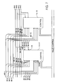
- FIG. 1 represents in block-diagram form one of the many types of automatic circuit testers in which the teachings of the present invention can be employed.
- the tester 10 tests a device under test (DUT) 12 by using digital test instruments in the form of driver/sensors 14 to apply signals to the DUT and observe the resulting signals that appear on the DUT.
- DUT device under test
- driver/sensors 14 to apply signals to the DUT and observe the resulting signals that appear on the DUT.
- a tester may also use analog instruments, such as a waveform generator 16 or a digital voltmeter 18.
- typical automatic test equipment employs a scanner 20 and a fixture 22.
- the scanner 20 provides a large number of fixed-position system pins 24, and these pins are used to carry signals to and from the DUT. However, they are not physically positioned to line up with test points on any particular circuit board, and signals on the system pins 24 have to be directed to different physical positions for every board type or family.
- the number of necessary nails 26 is very large, but only a small number of them are employed at any one time.
- a DUT may have a large number of components, which in total require a large number of test points, but each test of an individual component or circuit may involve only the test points that electrically communicate with the particular terminals of that component or circuit and a few others, whose operation must be affected in order to isolate that component or circuit.
- the tester leaves all other test points idle. Subsequently, when the system tests other components or circuits on the board, it uses another small subset of the test points and thus another small subset of the nails 26.
- the tester therefore includes the scanner 20, which is a matrix of switches and other circuitry that switches the connections between instruments and system pins 24 between bursts so that individual instruments can be used for different nails for different parts of a test.
- the control circuitry for the tester may be embodied in a computer 28, a sequencer 30, and a scanner driver 34.
- the computer 28 communicates with the scanner driver-34 by means of, for instance, industry-standard MXI and VXI buses 36 and 38 to specify the connections that the scanner 20 is to make between the instruments and the system pins 24.
- the scanner driver 34 responds by applying scanner-control signals to the scanner by means of a separate scanner bus to be described below.
- the VXI bus also serves as an instrument bus, carrying instrument-control signals such as those by which the computer 28 loads a pin memory 32 with values representing the signals that the individual test points are to receive or are expected to produce during the burst.
- the computer 28 may similarly program an analog instrument such as the digital voltmeter 18 if such an instrument is included as a standard part of the tester.
- an analog instrument such as the waveform generator 16, which may not be an ordinary part of the system and is not plugged into the VXI bus, may be connected to the scanner 20 and programmed separately, possibly by the computer 28.
- the computer 28 turns control over to the high-speed sequencer 30, which clocks the driver/sensors 14 and the pin memory 32 and may control other instruments as well.
- the computer 28 reads the results from the pin memories 32 and, for instance, the digital voltmeter 18 and uses appropriate equipment such as a display 40 to produce an indication of the results, either then or after further bursts.
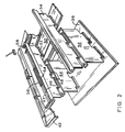
- FIG. 2 shows the physical arrangement that certain of the elements of FIG. 1 might assume in an embodiment of the present invention.
- FIG. 2 shows that the VXI bus 38 is provided, in the conventional manner, as a backplane bus lying in a horizontal plane near the bottom of a tester chassis 42.
- the driver/sensors 14 and digital voltmeter 18 of FIG. 1 are provided by a number of circuit boards plugged into the VXI backplane 38 to receive the instrument-control signals that program and otherwise control their operation.
- FIG. 2 depicts only one of those boards 44, but a typical tester will employ many such boards arrayed physically in parallel.
- FIG. 2 omits the connectors into which such further boards would be plugged.
- the circuit tester provides the scanner 20 in a plurality of circuit boards. Only two scanner boards 46 and 47 appear in FIG. 2, but the typical arrangement will employ a larger number. Also included in the scanner 20 of FIG. 1 is a scanner backplane bus 50, whose physical orientation is more or less parallel to that of the VXI bus 38. Scanner board 46 plugs into connectors 48 at the upper edge of board 44, where the board provides the ports at which the analog instrument or driver/sensors drive and/or sense signals. Scanner boards 46 and 47 also plug into connectors such as connector 51 on the scanner bus 50, from which they receive scanner-control signals. They also send and receive instrument and DUT signals over bus 50.
- FIG. 2 shows edge connectors 48 as making the connection between boards 44 and 46
- instrument boards not made by the tester manufacturer will not in general be arranged to mate in such a manner with the tester manufacturer's scanner boards.
- the tester manufacturer preferably makes the height of its own instrument boards greater than the standard VXI-board height. This will leave a space between the scanner-board lower edge and the upper edges of the other suppliers' (standard-height) instrument boards, where, say, coaxial-cable connections can be made between the boards.
- FIG. 2 does not show the largely conventional connection of the VXI backplane 38 to the MXI bus by which the computer 28 communicates with the scanner 20.
- the computer does send signals to the VXI backplane 38, and some of those signals, appropriately decoded, are forwarded to the scanner 20 by the scanner driver 34, which is shown in FIG. 2 as being embodied in a circuit board oriented parallel to scanner boards 46 and 48.
- a "slot zero" board 52 makes the connections between the VXI backplane 38 and the scanner driver 34.
- the upper edges of the scanner boards 46 and 47 provide connectors 54 and 56, which, together with corresponding connectors on other scanner boards not shown, contain part of the system pins 24 of FIG. 1. Also included on the upper edges of scanner boards 46 and 47 are connectors 58 for attaching coaxial cables from, for instance, the external waveform generator 16 of FIG. 1. (Of course, the waveform generator could be provided as the driver/sensors and the voltmeter are; i.e., it could be connected between a scanner board and the VXI bus.) It is through a discussion of the connection between the system pins and analog instruments such as the waveform generator 16 and the digital voltmeter 18 that the present invention will now be illustrated, although the broader principles of the invention can also be applied to connecting digital instruments.
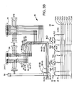
- FIGS. 3A and 3B depict in schematic form part of the switching functions performed by scanner board 46.
- the sixteen pairs of contacts 68 arrayed along the lower portions of FIGS. 3A and 3B represent contacts on the mating connectors 51 (FIG. 2) by which scanner board 46 is connected to eight pairs of conduction-path links in eight respective sequences of many links on the scanner backplane 50.
- the scanner backplane 50 also carries scanner-control signals on lines not shown in FIGS. 3A and 3B; i.e., the scanner backplane 50 provides a control bus as well as the signal bus that consists of the link sequences.
- Each sequence forms a conduction path that runs the length of the scanner bus 50 when its component links are connected in series by switches on the various scanner boards, which, as will be explained presently, act as connection modules for those link sequences.
- a first set of conductor links 70A-H extends to connector 51 from the next connector to the left on the scanner backplane 50.
- a second set of links 72A-H extends to connector 51 from the next connector to the right.
- a waveform generator connected to a scanner board disposed to the left of the scanner board 46 depicted in FIGS. 3A and 3B has placed a signal on conductor link 70A in a manner to be described below.
- this signal is to be forwarded to one of the system pins 24 on the scanner board depicted in FIGS. 3A and 3B.
- This result is achieved by operating first-link and second-link switches 74A and 76A and internal switch 78A, all of which are associated with the link sequence of which link 70A is a part (the "A sequence"). Specifically, switches 74A and 78A are closed, while switch 76A remains open. Also open is the internal switch 78E associated with the E sequence. The result of these switch states is that the signal from link 70A is steered to the upper circuitry in FIGS. 3A and 3B and is not forwarded to the next link 72A in the A sequence.
- the signal originates in a waveform generator connected to a scanner board to the right of the board in FIGS. 3A and 3B and that its destination is a scanner board to the left of that in FIGS. 3A and 3B; that is, the signal is not intended to be directed to any of the system pins 24 on board 26 of FIGS. 3A and 3B.
- internal switch 78A is opened, and the first-link and second-link switches 74A and 76A are both closed so as to connect first link 70A to second link 72A through the common node to which switches 70A and 72A are connected. That is, the board illustrated in FIGS. 3A and 3B acts to provide continuity in the otherwise interrupted A sequence, which includes links 70A and 72A.
- a waveform-generator signal comes from the upper circuitry in FIGS. 3A and 3B in a manner that will be described later.
- this signal is to be forwarded to a system pin 24 on a scanner board to the left of that depicted in FIGS. 3A and 3B.
- the signal is to be sent to the left along the A sequence of links, i.e., along link 70A.
- internal switch 78E is open, internal switch 78A is closed, first-link switch 74A is closed, and second-link switch 76A is open.
- This transmission scheme is that it automatically adjusts the length of the signal path so as to minimize stub lengths. Specifically, when signals are to be transmitted from one scanner board to another, only the scanner-bus links disposed between those two boards are connected; the other scanner-bus links are isolated from those links, so the reflections that would otherwise result are avoided despite the common-path feature that results from a bus organization.
- FIGS. 3A and 3B These matrices represent four parallel tree structures. Each tree structure has a respective one of four internal "trunk" conductors 80A-D at its lowest level.
- Conductor 80A the trunk of the first tree, is associated with the A and E sequences of links.
- conductor 80B is associated with the B and F sequences, conductor 80C with the C and G sequences, and conductor 80D with the D and H sequences.
- trunk conductor 80A at the lowest level of the A tree fans out to four "limb" conductors 84-1A, 84-2A, 84-3A, and 84-4A at the next higher level.
- Limb conductors 84-3A and 84-4A lead directly to coaxial-cable connectors 58, while connectors 84-1A and 84-2A both fan out further.
- tree switches 86-1A, 86-2A, 86-3A, and 86-4A for instance, limb conductor 84-1A fans out to four "branch" conductors 88-1A, 88-2A, 88-3A, and 88-4A.
- Each of these branch conductors fans out to four respective system pins 24.
- conductor 88-1A fans out to four respective system pins 24-1, 24-2, 24-3, and 24-4.
- trunk conductor 80A can be connected to any of the system pins 24 through a proper selection of switch closures. Since trunk conductor 80A can in turn be connected to left link 70A or 70E or to right link 72A or 72E, signals on the A and E sequences can be steered to any of the system pins 24. Inspection of FIGS. 3A and 3B reveals that each of the other trunk conductors 80B, 80C, and 80D can similarly be connected through a respective parallel tree to any of the system pins 24, so the system pins can additionally be connected to the link sequences associated with those trunk conductors.
- the trunk conductors 80 can be connected selectively not only to the system pins but also to the analog instruments to which the scanner is connected. Switches such as switch 82-3A can connect a trunk conductor to a limb conductor such as conductor 84-3A, which leads to an analog instrument. If board 44 is an analog-instrument board, conductor 84-3A leads to the lower-edge contact pads that the instrument-board connector 48 (FIG. 2) receives. In order to show the range of features that a scanner board might have, however, FIG. 3A includes driver-sensor signal paths, which a scanner board of the type connected to a driver/sensor board would include. Such a scanner board would have its analog-instrument paths such as conductor 84-3A connected to the upper-edge connector 58, so FIG. 3A shows such a connection.
- the scanner bus can provide connections to as many as eight different instruments, although the system pins 24 on a single scanner board can be connected to only four of them at the same time.
- conductors 88-5A, 88-5B, 88-5C, and 88-5D represent the beginnings of paths that the tester provides to separate instruments on other boards when proper connections are made.
- the DUT conductor path 96-17 associated with system pin 24-17 can be connected to any one of four instrument conduction paths that begin with respective branch conductors 88-5A, 88-5B, 88-5C, and 88-5D.
- FIGS. 3A and 3B include the signal paths and other circuitry that would be provided by a scanner board of the type intended for connection to a driver/sensor board, which contains a group of digital instruments, i.e., driver/sensors.
- a scanner board of the type intended for connection to a driver/sensor board, which contains a group of digital instruments, i.e., driver/sensors.
- each of the system pins 24 is connectable not only to the analog instruments to which connector 58 and the scanner bus 50 provide connection but also to a respective dedicated driver/sensor on board 44.
- closure of a switch 102-1 connects system pin 24-1 to a conductor 100-1 that leads to a driver/sensor on board 44.
- an overvoltage-protection circuit provided on board 46 but not shown in the drawings, can be connected to system pin 24-1 by operation of a switch not shown in FIG. 3A but designated switch 104-1 in FIG 6.
- the board provides further switches 106-1 and 108-1.
- the scanner board 46 For each of the thirty-two system pins 24, therefore, the scanner board 46 must provide eight switches: a driver/sensor switch such as switch 102-1, an overvoltage-protector switch such as switch 104-1 (FIG. 6), two isolation switches such as switches 106-1 and 108-1, and four matrix/tree switches such as switches 90-1A, 90-1B, 90-1C, and 90-1D. These are required in addition to the lower-level tree switches and the switches for selecting the mode of connection to the scanner bus 50.
- the scanner provides this large number of switches as mechanical relays, which, because of their size, can present layout and stub-length problems.
- a structure of the type depicted in FIG. 4 reduces both the layout and the stub-length problems by extending the layout into a third dimension.
- the resulting arrangement simplifies the layout problem so as to enable the designer to provide more channels than an equivalent-sized two-dimensional layout would permit, and it reduces to a fraction the stub length required to provide the flexible layout illustrated in FIGS. 3A and 3B.
- FIG. 4 depicts representative parts of scanner board 46, showing two connectors 110 and 112 by which it plugs into the driver/sensor board 44.
- FIG. 4 also depicts the connector 51 by which board 46 plugs into the scanner bus 50.
- the various layers of (multi-layer) board 46 provide many of the conduction paths depicted in FIGS. 3A and 3B.
- auxiliary boards 114 which in turn are mounted on the main board 46 and extend transversely from its surface.
- auxiliary boards 114-1 through 114-50 There are fifty auxiliary boards, labeled 114-1 through 114-50, of which FIG. 4 shows only seven.
- Boards 114-1 through 114-46 contain eight relays apiece.
- Boards 114-47 through 114-50 contain six apiece.
- Each board also contains circuitry, such as integrated circuits 116 and 118 on board 114-10, for controlling the relays on that auxiliary board.
- Circuitry provided on the main board 46 but not shown in the drawings receives instructions coupled to it by means of connector 51 from the scanner bus 50, which in turn receives those signals from the computer 28 by way of the scanner driver 34 (FIG. 2), the "slot zero" board 52 (FIG. 2), and buses 36 and 38 (FIG. 1).
- This circuitry receives signals from the computer 28 that designate the states that the relays are to assume, and it drives the relays so that they assume the proper states.
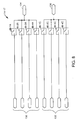
- FIG. 5 shows the interconnection of the next four boards 114-9, 114-10, 114-11, and 114-12, which contain the sixteen relays 90-1A through 90-1D, 90-2A through 90-2D, 90-3A through 90-3D, and 90-4A through 90-4D that interconnect system pins 24-1, 24-2, 24-3, and 24-4 with branch conductors 88-1A through 88-1D.
- the main board contains branch conductive paths 88-1A, 88-1B, 88-1C, and 88-1D, to which corresponding terminals in each of auxiliary boards 114-9 through 114-12 are connected.
- FIG. 6, which is a schematic diagram of the switching connections on board 114-9, depicts these terminals 120 on board 114-9 and shows that they lead to the matrix switches 90-1A, 90-1B, 90-1C, and 90-1D, which auxiliary board 114-9 provides.
- Another terminal 122 connects isolation relay 106-1 to system pin 24-1 by way of the main board, while yet another terminal 124 connects relay 102-1 to driver/sensor pin 100-1 by way of the main board.
- Further terminals 126 and 128 provide the connections between the auxiliary board 114-9 and the overvoltage-protection circuitry on the main board 46.
- FIG. 6 omits the relay-driver and other control connections needed to interpret and retain instructions regarding the required relay states. Raising these connections, as well as the connections illustrated in FIG. 6, out of the plane of the main board 46 greatly simplifies the conduction-path layout and, as will be explained later in greater detail, reduces the stub lengths required-to achieve circuit versatility.
- Auxiliary boards 114-10, 114-11, and 114-12 are identical to board 114-9; each provides the switching necessary to connect its associated system pin 24 to one of the trees through their respective branch conductors 88-1A, 88-1B, 88-1C, and 88-1D, each of which fans out into four system pins.
- the outputs of these groups of switches are eight four-conductor groups such as group 88-1 of FIG. 5, each of which contains four corresponding branch conductors, one for each of the four trees.
- FIG. 7 shows four of these four-conductor groups 88-1, 88-2, 88-3, and 88-4 leading to two auxiliary boards 114-17 and 114-18.
- the other four four-conductor groups lead in an identical manner to the thirty-fifth and thirty-sixth auxiliary boards 114, which are not shown in the drawings.
- These four boards contain the relays 86 that provide the concentration from the branch conductors 88 to the limb conductors 84.
- FIG. 8 is a schematic diagram of the internal switch arrangement of auxiliary board 114-17.
- Terminals 130 of auxiliary board 114-17 receive the A-tree conductors from the four branch-conductor groups that lead to boards 114-17 and 114-18, while terminals 132 of that board receive the C-tree conductors from those groups.
- Corresponding terminals on board 114-18 receive the B-tree and D-tree conductors, respectively, from those groups.
- the identical pair of auxiliary boards that receives the other four branch-conductor groups segregates the A, B, C, and D conductors similarly.
- Board 114-17 concentrates its eight branches into two limbs in a manner that is apparent from its schematic diagram in FIG. 8, which identifies its relays in accordance with the numbering scheme followed in FIGS. 3A and 3B.
- FIG. 9 depicts auxiliary board 114-45, whose terminals 138 are connected to the limb conductor 84-1A from terminal 134 (FIG. 8) of auxiliary board 114-17, limb conductor 84-2A from the corresponding terminal on the thirty-fifth auxiliary board, and two lines 84-3A and 84-4A from two of the coaxial-cable connectors 58.
- Board 114-45 provides the concentration of all of the A-tree limb conductors into the A-tree trunk conductor 80A.
- Board 114-45 also receives all of the C-tree limb conductors at its terminals 140 and provides the concentration into the C-tree trunk conductor 80C.
- Board 114-45 is identical internally to the board 114-17 depicted in FIG. 8, but FIG. 10 depicts its internal connections schematically in order to show the correspondence of its relays to those depicted in FIGS. 3A and 3B.
- the forty-sixth auxiliary board performs a similar concentration function for the B and D trees.
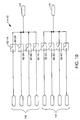
- each of the "trunk" conductors 80A-D can be connected selectively to two links in each of two respective link sequences.
- a separate auxiliary card for each tree provides the relays that perform this switching.
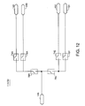
- FIGS. 11 and 12 depict one of those auxiliary boards 114-50, whose relays perform this switching for the A tree. Board 114-50 is internally identical to the forty-seventh, forty-eighth, and forty-ninth boards, which perform the same junctions for the D, C, and B trees, respectively.
- a common terminal 146 is connected to the trunk conductor 80A of the A tree.
- auxiliary-board terminal 148 provides the connection from relay 74A to the conductor path on the main board that leads to the main-board terminal 68 by which the main board is connected to link 70A.
- terminals 150, 152, and 154 provide the connections to links 72A, 70E, and 72E, respectively.
- the sixteen relays 90-1A through 90-1D, 90-2A through 90-2D, 90-3A through 90-3D, and 90-4A through 90-4D form a cross-point matrix of switches that perform what can be thought of as a reciprocal treeing operation: not only can a branch 88-1 of a given tree be connected to any one of four system pins 24-1 through 24-4, but any of those system pins can also be connected to top branch 88-1 of any of the four trees.
- Each of these selections results in transmission stubs; that is, although a main path is formed through the closed switch, a stub path branches from the main path to the open switches. It is important to keep these stub lengths short enough that the round-trip propagation time through them is short in comparison with the rise times of the signals that the system is intended to handle.
- relay 90-4A will be closed, while relays 90-4B, 90-4C, and 90-4D will be open.
- a stub will accordingly be present on conductor 96-4, which, as FIG. 4 shows, is T-shaped.
- the signal path that includes conductor 96-4 appears at the bottom of board 114-12 and forks when it reaches the top of that board.
- the signal is intended to proceed to the left to one side of relay 90-4A, which directs it to branch conductor 88-1A.
- the signal also propagates to the right until it reaches the open relay 90-4D, which reflects it.
- the signal received from system pin 24-4 (FIG. 3A) is intended to propagate from the bottom of relay 90-4A on board 114-12 to the right along conductor 88-1A to board 114-17, it also propagates to the left along conductor 88-1A until it reaches open relay 90-1A on auxiliary board 114-9, from which it reflects back to the right. It is important for this reflection time to be short, and it therefore is also important for the stub length determined by the distance between the corresponding ends of relays 90-1A and 90-4A to be short. It would be virtually impossible to accomplish this goal and keep the stub on branch conductor 88-1A short, too, in a two-dimensional layout.
- stubs on both conductors can be kept short simultaneously by placing auxiliary boards 114-9 through 114-12 on their edges, physically in parallel, and relatively close together.
- a three-dimensional layout thus yields a higher packaging density and hence shorter signal stubs.
Landscapes
- Engineering & Computer Science (AREA)
- General Engineering & Computer Science (AREA)
- Computer Hardware Design (AREA)
- Microelectronics & Electronic Packaging (AREA)
- Physics & Mathematics (AREA)
- General Physics & Mathematics (AREA)
- Tests Of Electronic Circuits (AREA)
Claims (5)
- Automatische Schaltungsprüfeinrichtung (10) mit:
Systemstiften (24), die zum Verbinden mit Prüfpunkten in einer zu prüfenden Vorrichtung (12) geeignet sind;
Meßgeräten (14, 16, 18) zum Erzeugen von Signalen oder zum Überwachen von an diese angelegten Signalen;
mindestens drei Verbindungsmodulen (74A-H, 76A-H, 78A-H), von denen jeweils mindestens drei mindestens einem entsprechenden aus einer Vielzahl von Prüfeinrichtungshilfsmitteln (14, 16, 18, 24) zugeordnet sind, wobei mindestens eines der Prüfeinrichtungshilfsmittel ein Systemkontaktstift (24) und mindestens ein anderes der Prüfeinrichtungshilfsmittel eines der Meßgeräte (14, 16, 18) ist; und
einer Steuerschaltung (28, 30, 34), die zum selektiven Annehmen eines aus einer Vielzahl von Steuerzuständen eingerichtet ist;
dadurch gekennzeichnet, daß:A) die Prüfeinrichtung ferner einen Signalbus (50) mit mindestens einer Busleitung aufweist, wobei mindestens eine der Busleitungen unterbrochen ist, um eine geordnete Serie von Verbindungen (70A-H, 72A-H) zu bilden, wobei jede der Verbindungen ein erstes und ein zweites Ende hat, die sich gegenüberliegen;B) jedes der Verbindungsmodule (74A-H, 76A-H, 78A-H) einem entsprechenden Paar erster (70A-H) und zweiter (72A-H) benachbarter Verbindungen zugeordnet ist, die mit dem zweiten Ende der ersten Verbindung des ihm zugeordneten Paares und mit dem ersten Ende der zweiten Verbindung des ihm zugeordneten Paares verbunden werden, wobei jedes Verbindungsmodul in einem ersten, zweiten und dritten Modulzustand betriebsfähig ist, so daß:i. in seinem ersten Modulzustand jedes Verbindungsmodul das zweite und das erste Ende der ersten bzw. der zweiten Verbindung eines Paares von ihm zugeordneten Verbindungen miteinander koppelt, um Durchgang zwischen diesen Verbindungen herzustellen, sie jedoch von jedem ihm zugeordneten Prüfeinrichtungshilfsmittel zu trennen;ii. in seinem zweiten Modulzustand jedes Verbindungsmodul das zweite Ende der ersten ihm zugeordneten Verbindung mit einem ihm zugeordneten Prüfeinrichtungshilfsmittel verbindet und das erste Ende der zweiten ihm zugeordneten Verbindung vom ersten Ende und von jedem ihm zugeordneten Prüfeinrichtungshilfsmittel trennt; undiii. in seinem dritten Zustand jedes Verbindungsmodul das erste Ende der zweiten ihm zugeordneten Verbindung mit einem ihm zugeordneten Prüfeinrichtungshilfsmittel koppelt und das zweite Ende der ersten ihm zugeordneten Verbindung von jedem ihm zugeordneten Prüfeinrichtungshilfsmittel und von der zweiten ihm zugeordneten Verbindung trennt; undC) jeder aus der Vielzahl von Steuerzuständen der Steuerschaltung einem anderen Paar von Verbindungsmodulen zugeordnet ist; undD) die Steuerschaltung eines der zugeordneten Paare von Verbindungsmodulen in seinen zweiten Zustand, den anderen in seinen dritten Zustand und alle Verbindungsmodule zwischen den Modulen, die diesem Steuerzustand zugeordnet sind, in ihre ersten Zustände schaltet, wodurch in jedem Steuerzustand die Prüfeinrichtung einen Signalweg zwischen Prüfeinrichtungshilfsmitteln, die den Verbindungsmodulen zugeordnet sind, die diesem Steuerzustand zugeordnet sind, herstellt, während sie diese Hilfsmittel von Verbindungen im Bus jenseits des Teils davon trennt, wobei die Verbindung zwischen den Verbindungsmodulen, die diesem Steuerzustand zugeordnet sind, hergestellt wird. - Automatische Schaltungsprüfeinrichtung nach Anspruch 1, wobei:A) eine Vielzahl von Busleitungen eines Signalbusses (50) unterbrochen werden, um jeweils eine Vielzahl von geordneten Serien von Verbindungen (70A-H, 72A-H) mit jeder der Verbindungen mit einem ersten (70A-H) und einem zweiten (72A-H) Ende, die sich gegenüberliegen, zu bilden; undB) jeder Verbindungsmodul (74A-H, 76A-H, 78A-H) einem Paar erster und zweiter benachbarter Verbindungen in der Serie von Verbindungen, das Teil einer Busleitung (z.B. 70A und 72A) ist, zugeordnet ist und jeweils Paaren erster und zweiter benachbarten Verbindungen in der Serie von Verbindungen zugeordnet ist, die Teile von anderen Busleitungen (z.B. 70B und 72B, 70C und 72C, 70D und 72D) sind, wobei der Verbindungsmodul mit dem zweiten Ende der ersten Verbindung jedes ihm zugeordneten Paares und mit dem ersten Ende der zweiten Verbindung jedes ihm zugeordneten Paares verbunden wird; undC) jedes Verbindungsmodul in einem ersten, zweiten und dritten Modulzustand mit jeder der geordneten Serien von Verbindungen, der er zugeordnet ist, betriebsfähig ist.
- Automatische Schaltungsprüfeinrichtung nach Anspruch 1 oder 2 mit:A) einer im allgemeinen ebenen Scanner-Rückwandplatine (50). die den Signalbus darstellt; undB) einer Vielzahl von im allgemeinen ebenen Leiterplatten (46, 47), die mit der Scanner-Rückwandplatine so verbunden sind, daß sie sich quer zu dieser erstrecken, wobei jede Leiterplatte einen anderen der Verbindungsmodule darstellt.
- Automatische Schaltungsprüfeinrichtung nach Anspruch 1 oder 3, wobei jedes Modul aufweist:A) einen gemeinsamen Knoten;B) einen internen Knoten, der durch dieses Modul mit ihm zugeordneten Prüfeinrichtungshilfsmittel verbindbar ist;C) einen Erstverbindungsschalter, der jeder ersten Verbindung zugeordnet ist, die diesem Modul zugeordnet ist, und der zwischen die zugeordnete erste Verbindung und den gemeinsamen Knoten geschaltet ist, wobei der Erstverbindungsschalter im ersten und im zweiten Zustand dieses Moduls geschlossen ist und in seinem dritten Zustand geöffnet ist;D) einen Zweitverbindungsschalter, der der zweiten Verbindung zugeordnet ist, der dieser Modul zugeordnet ist, und der zwischen die zugeordnet zweite Verbindung und den gemeinsamen Knoten geschaltet ist, wobei der Zweitverbindungsschalter im ersten und im dritten Modulzustand dieses Moduls geschlossen ist und in seinem zweiten Modulzustand geöffnet ist; undE) einen internen Schalter, der zwischen den gemeinsamen Knoten und den internen Knoten geschaltet ist, wobei der interne Schalter im ersten Modulzustand dieses Moduls geöffnet ist und in seinem zweiten und dritten Modulzustand geschlossen ist.
- Automatische Schaltungsprüfeinrichtung nach Anspruch 4, wobei jeder Modul ferner aufweist:A) einen gemeinsamen Knoten, der jeder Serie von Verbindungen zugeordnet ist; undB) einen internen Schalter (78A-H), der jeder Serie von Verbindungen zugeordnet ist und zwischen den gemeinsamen Knoten, der dieser Serie von Verbindungen zugeordnet ist, und den internen Knoten. der dieser Serie von Verbindungen zugeordnet ist, geschaltet ist, wobei jeder interne Schalter im ersten Modulzustand geöffnet ist und im zweiten und dritten Zustand geschlossen ist; und ferner istC) der Erstverbindungsschalter (74A-H), der jeder ersten Verbindung (70A-H) gehört, die diesem Modul zugeordnet ist, zwischen die zugeordnete erste Verbindung (70A-H) und den gemeinsamen Knoten, der der Serie zugeordnet ist, von der die zugeordnete erste Verbindung ein Teil ist, geschaltet, wobei jeder Erstverbindungsschalter im ersten und im zweiten Zustand dieses Moduls, die den Serienverbindungen zugeordnet sind, zu denen die erste Verbindung gehört, der dieser Erstverbindungsschalter zugeordnet ist, geschlossen ist und in seinem dritten Zustand, der dieser gleichen Serie von Verbindungen zugeordnet ist, geöffnet ist; undD) der Zweitverbindungsschalter (76A-H), der jeder zweiten Verbindung (72A-H) zugeordnet ist, der dieser Modul zugeordnet ist, zwischen die zugeordnete zweite Verbindung und den gemeinsamen Knoten, der der Serie von Verbindungen zugeordnet ist, von der die zugeordnete zweite Verbindung ein Teil ist, verbunden, wobei der Zweitverbindungsschalter im ersten und im zweiten Modulzustand dieses Moduls, der der Serie von Verbindungen zugeordnet ist, zu der die zweite Verbindung gehört, der dieser Zweitverbindungsschalter zugeordnet ist, geschlossen ist und in seinem zweiten Modulzustand, der dieser gleichen Serie von Verbindungen zugeordnet ist, geöffnet ist.
Applications Claiming Priority (2)
| Application Number | Priority Date | Filing Date | Title |
|---|---|---|---|
| US659755 | 1991-02-22 | ||
| US07/659,755 US5124636A (en) | 1991-02-22 | 1991-02-22 | Tester interconnect system |
Publications (2)
| Publication Number | Publication Date |
|---|---|
| EP0502624A1 EP0502624A1 (de) | 1992-09-09 |
| EP0502624B1 true EP0502624B1 (de) | 1995-12-20 |
Family
ID=24646697
Family Applications (1)
| Application Number | Title | Priority Date | Filing Date |
|---|---|---|---|
| EP92301302A Expired - Lifetime EP0502624B1 (de) | 1991-02-22 | 1992-02-18 | Verbindungsanordnung für Prüfeinrichtung |
Country Status (4)
| Country | Link |
|---|---|
| US (1) | US5124636A (de) |
| EP (1) | EP0502624B1 (de) |
| JP (1) | JP3285212B2 (de) |
| DE (1) | DE69206848T2 (de) |
Families Citing this family (19)
| Publication number | Priority date | Publication date | Assignee | Title |
|---|---|---|---|---|
| US5534774A (en) * | 1992-04-23 | 1996-07-09 | Intel Corporation | Apparatus for a test access architecture for testing of modules within integrated circuits |
| US5406197A (en) * | 1992-07-31 | 1995-04-11 | International Business Machines Corporation | Apparatus for controlling test inputs of circuits on an electronic module |
| US6101457A (en) * | 1992-10-29 | 2000-08-08 | Texas Instruments Incorporated | Test access port |
| US5752216A (en) * | 1994-07-06 | 1998-05-12 | Dimensions International, Inc. | Non-intrusive data interface system for air traffic control |
| US6175230B1 (en) * | 1999-01-14 | 2001-01-16 | Genrad, Inc. | Circuit-board tester with backdrive-based burst timing |
| US6552528B2 (en) * | 2001-03-15 | 2003-04-22 | Advantest Corporation | Modular interface between a device under test and a test head |
| US8161144B2 (en) * | 2001-08-15 | 2012-04-17 | National Instruments Corporation | Defining a switch device route based on required signal characteristics and resource dependencies |
| US20030043757A1 (en) * | 2001-08-15 | 2003-03-06 | Jason White | Optimizing switch device route transitions |
| US6954904B2 (en) | 2001-08-15 | 2005-10-11 | National Instruments Corporation | Creating a graphical program to configure one or more switch devices |
| US7017138B2 (en) * | 2001-08-15 | 2006-03-21 | National Instruments Corporation | Dynamically determining a route through one or more switch devices at program execution time |
| US7062719B2 (en) | 2001-08-15 | 2006-06-13 | National Instruments Corporation | Graphically defining a route through one or more switch devices |
| US6701270B1 (en) * | 2001-09-20 | 2004-03-02 | Lsi Logic Corporation | Method for reliability testing leakage characteristics in an electronic circuit and a testing device for accomplishing the source |
| US20050232256A1 (en) * | 2002-03-29 | 2005-10-20 | Jason White | Applying object oriented concepts to switch system configurations |
| US7154257B2 (en) * | 2002-09-30 | 2006-12-26 | Intel Corporation | Universal automated circuit board tester |
| US6999888B2 (en) * | 2002-09-30 | 2006-02-14 | Intel Corporation | Automated circuit board test actuator system |
| US6958598B2 (en) * | 2003-09-30 | 2005-10-25 | Teradyne, Inc. | Efficient switching architecture with reduced stub lengths |
| US7279919B2 (en) * | 2005-01-14 | 2007-10-09 | Verigy (Singapore) Pte. Ltd. | Systems and methods of allocating device testing resources to sites of a probe card |
| ES2303415B2 (es) * | 2005-10-20 | 2010-03-04 | Universidad De Malaga | Banco de ensayos automatizado para ensayos de rutina segun dc 73/23/cee. |
| CN102565518A (zh) * | 2010-12-16 | 2012-07-11 | 鸿富锦精密工业(深圳)有限公司 | 电流平衡测试系统 |
Family Cites Families (7)
| Publication number | Priority date | Publication date | Assignee | Title |
|---|---|---|---|---|
| US3854125A (en) * | 1971-06-15 | 1974-12-10 | Instrumentation Engineering | Automated diagnostic testing system |
| DE2909268C2 (de) * | 1979-03-09 | 1980-09-11 | Wandel & Goltermann Gmbh & Co, 7412 Eningen | Verfahren und Einrichtung zur Oberwachung der Funktion der in einem MeIistellenumschalter befindlichen Schalter |
| US4354268A (en) * | 1980-04-03 | 1982-10-12 | Santek, Inc. | Intelligent test head for automatic test system |
| US4724379A (en) * | 1984-03-14 | 1988-02-09 | Teradyne, Inc. | Relay multiplexing for circuit testers |
| US4746855A (en) * | 1984-03-14 | 1988-05-24 | Teradyne, Inc. | Relay multiplexing for circuit testers |
| US4719459A (en) * | 1986-03-06 | 1988-01-12 | Grumman Aerospace Corporation | Signal distribution system switching module |
| US4989202A (en) * | 1988-10-14 | 1991-01-29 | Harris Corporation | ISDN testing device and method |
-
1991
- 1991-02-22 US US07/659,755 patent/US5124636A/en not_active Expired - Lifetime
-
1992
- 1992-02-18 DE DE69206848T patent/DE69206848T2/de not_active Expired - Lifetime
- 1992-02-18 EP EP92301302A patent/EP0502624B1/de not_active Expired - Lifetime
- 1992-02-20 JP JP03326492A patent/JP3285212B2/ja not_active Expired - Lifetime
Also Published As
| Publication number | Publication date |
|---|---|
| EP0502624A1 (de) | 1992-09-09 |
| JPH04323577A (ja) | 1992-11-12 |
| US5124636A (en) | 1992-06-23 |
| DE69206848T2 (de) | 1996-08-29 |
| JP3285212B2 (ja) | 2002-05-27 |
| DE69206848D1 (de) | 1996-02-01 |
Similar Documents
| Publication | Publication Date | Title |
|---|---|---|
| US5124638A (en) | Automatic circuit tester employing a three-dimensional switch-matrix layout | |
| US5124636A (en) | Tester interconnect system | |
| US5101150A (en) | Automatic circuit tester with separate instrument and scanner buses | |
| CA1208373A (en) | Integrated circuit test apparatus | |
| JP2641214B2 (ja) | 回路試験方法 | |
| KR0163756B1 (ko) | 전자 모듈 소켓장치 | |
| US5717329A (en) | Analog autonomous test bus framework for testing integrated circuits on a printed circuit board | |
| US4348759A (en) | Automatic testing of complex semiconductor components with test equipment having less channels than those required by the component under test | |
| US5162728A (en) | Functional at speed test system for integrated circuits on undiced wafers | |
| GB2322203A (en) | Integrated circuit device tester | |
| JPH01501033A (ja) | 素早い注文設計及び独特な試験能力の為の集積回路パッケージ形式 | |
| US5068602A (en) | DUT board for a semiconductor device tester having a reconfigurable coaxial interconnect grid and method of using same | |
| US6964574B2 (en) | Daughter board for a prototyping system | |
| JPS62212757A (ja) | 信号分散システムスイツチングモジユ−ル | |
| US6181146B1 (en) | Burn-in board | |
| US7511517B2 (en) | Semi-automatic multiplexing system for automated semiconductor wafer testing | |
| US5132614A (en) | Semiconductor device and method and apparatus for testing the same | |
| EP0682259A1 (de) | Schaltungstesthalterung mit zusammengeschalteten Sonden | |
| JP3037043B2 (ja) | プリント基板のテスト容易化回路実装方式 | |
| KR100761894B1 (ko) | 반도체 디바이스 시험장치 및 디바이스 인터페이스 보드 | |
| US6507205B1 (en) | Load board with matrix card for interfacing to test device | |
| HK1002259B (en) | Automatic circuit tester with separate instrument and scanner busses | |
| CN219266942U (zh) | 一种导控计算机测试平台的自检系统 | |
| CN220629352U (zh) | 一种基于vpx平台架构的高密度高速互联通道测试装置 | |
| JPS6421374A (en) | Apparatus for testing integrated circuit |
Legal Events
| Date | Code | Title | Description |
|---|---|---|---|
| PUAI | Public reference made under article 153(3) epc to a published international application that has entered the european phase |
Free format text: ORIGINAL CODE: 0009012 |
|
| AK | Designated contracting states |
Kind code of ref document: A1 Designated state(s): DE FR GB |
|
| 17P | Request for examination filed |
Effective date: 19921012 |
|
| 17Q | First examination report despatched |
Effective date: 19940617 |
|
| GRAA | (expected) grant |
Free format text: ORIGINAL CODE: 0009210 |
|
| AK | Designated contracting states |
Kind code of ref document: B1 Designated state(s): DE FR GB |
|
| REF | Corresponds to: |
Ref document number: 69206848 Country of ref document: DE Date of ref document: 19960201 |
|
| ET | Fr: translation filed | ||
| PLBE | No opposition filed within time limit |
Free format text: ORIGINAL CODE: 0009261 |
|
| 26N | No opposition filed | ||
| REG | Reference to a national code |
Ref country code: GB Ref legal event code: IF02 |
|
| PGFP | Annual fee paid to national office [announced via postgrant information from national office to epo] |
Ref country code: FR Payment date: 20100303 Year of fee payment: 19 |
|
| PGFP | Annual fee paid to national office [announced via postgrant information from national office to epo] |
Ref country code: DE Payment date: 20100226 Year of fee payment: 19 Ref country code: GB Payment date: 20100224 Year of fee payment: 19 |
|
| GBPC | Gb: european patent ceased through non-payment of renewal fee |
Effective date: 20110218 |
|
| REG | Reference to a national code |
Ref country code: FR Ref legal event code: ST Effective date: 20111102 |
|
| REG | Reference to a national code |
Ref country code: DE Ref legal event code: R119 Ref document number: 69206848 Country of ref document: DE Effective date: 20110901 |
|
| PG25 | Lapsed in a contracting state [announced via postgrant information from national office to epo] |
Ref country code: FR Free format text: LAPSE BECAUSE OF NON-PAYMENT OF DUE FEES Effective date: 20110228 |
|
| PG25 | Lapsed in a contracting state [announced via postgrant information from national office to epo] |
Ref country code: GB Free format text: LAPSE BECAUSE OF NON-PAYMENT OF DUE FEES Effective date: 20110218 |
|
| PG25 | Lapsed in a contracting state [announced via postgrant information from national office to epo] |
Ref country code: DE Free format text: LAPSE BECAUSE OF NON-PAYMENT OF DUE FEES Effective date: 20110901 |