EP0501279A1 - Microwave heterojunction bipolar transistors suitable for low-power, low-noise and high-power applications and method for fabricating same - Google Patents
Microwave heterojunction bipolar transistors suitable for low-power, low-noise and high-power applications and method for fabricating same Download PDFInfo
- Publication number
- EP0501279A1 EP0501279A1 EP92102659A EP92102659A EP0501279A1 EP 0501279 A1 EP0501279 A1 EP 0501279A1 EP 92102659 A EP92102659 A EP 92102659A EP 92102659 A EP92102659 A EP 92102659A EP 0501279 A1 EP0501279 A1 EP 0501279A1
- Authority
- EP
- European Patent Office
- Prior art keywords
- emitter
- layer
- heterojunction bipolar
- base
- microwave
- Prior art date
- Legal status (The legal status is an assumption and is not a legal conclusion. Google has not performed a legal analysis and makes no representation as to the accuracy of the status listed.)
- Withdrawn
Links
Images




Classifications
-
- H—ELECTRICITY
- H10—SEMICONDUCTOR DEVICES; ELECTRIC SOLID-STATE DEVICES NOT OTHERWISE PROVIDED FOR
- H10D—INORGANIC ELECTRIC SEMICONDUCTOR DEVICES
- H10D10/00—Bipolar junction transistors [BJT]
- H10D10/01—Manufacture or treatment
- H10D10/021—Manufacture or treatment of heterojunction BJTs [HBT]
-
- H—ELECTRICITY
- H10—SEMICONDUCTOR DEVICES; ELECTRIC SOLID-STATE DEVICES NOT OTHERWISE PROVIDED FOR
- H10D—INORGANIC ELECTRIC SEMICONDUCTOR DEVICES
- H10D10/00—Bipolar junction transistors [BJT]
-
- H—ELECTRICITY
- H10—SEMICONDUCTOR DEVICES; ELECTRIC SOLID-STATE DEVICES NOT OTHERWISE PROVIDED FOR
- H10D—INORGANIC ELECTRIC SEMICONDUCTOR DEVICES
- H10D10/00—Bipolar junction transistors [BJT]
- H10D10/01—Manufacture or treatment
-
- H—ELECTRICITY
- H10—SEMICONDUCTOR DEVICES; ELECTRIC SOLID-STATE DEVICES NOT OTHERWISE PROVIDED FOR
- H10D—INORGANIC ELECTRIC SEMICONDUCTOR DEVICES
- H10D10/00—Bipolar junction transistors [BJT]
- H10D10/80—Heterojunction BJTs
- H10D10/821—Vertical heterojunction BJTs
-
- H—ELECTRICITY
- H10—SEMICONDUCTOR DEVICES; ELECTRIC SOLID-STATE DEVICES NOT OTHERWISE PROVIDED FOR
- H10D—INORGANIC ELECTRIC SEMICONDUCTOR DEVICES
- H10D62/00—Semiconductor bodies, or regions thereof, of devices having potential barriers
- H10D62/10—Shapes, relative sizes or dispositions of the regions of the semiconductor bodies; Shapes of the semiconductor bodies
- H10D62/13—Semiconductor regions connected to electrodes carrying current to be rectified, amplified or switched, e.g. source or drain regions
- H10D62/133—Emitter regions of BJTs
-
- H—ELECTRICITY
- H10—SEMICONDUCTOR DEVICES; ELECTRIC SOLID-STATE DEVICES NOT OTHERWISE PROVIDED FOR
- H10D—INORGANIC ELECTRIC SEMICONDUCTOR DEVICES
- H10D62/00—Semiconductor bodies, or regions thereof, of devices having potential barriers
- H10D62/10—Shapes, relative sizes or dispositions of the regions of the semiconductor bodies; Shapes of the semiconductor bodies
- H10D62/13—Semiconductor regions connected to electrodes carrying current to be rectified, amplified or switched, e.g. source or drain regions
- H10D62/133—Emitter regions of BJTs
- H10D62/136—Emitter regions of BJTs of heterojunction BJTs
-
- H—ELECTRICITY
- H10—SEMICONDUCTOR DEVICES; ELECTRIC SOLID-STATE DEVICES NOT OTHERWISE PROVIDED FOR
- H10D—INORGANIC ELECTRIC SEMICONDUCTOR DEVICES
- H10D62/00—Semiconductor bodies, or regions thereof, of devices having potential barriers
- H10D62/10—Shapes, relative sizes or dispositions of the regions of the semiconductor bodies; Shapes of the semiconductor bodies
- H10D62/13—Semiconductor regions connected to electrodes carrying current to be rectified, amplified or switched, e.g. source or drain regions
- H10D62/137—Collector regions of BJTs
-
- H—ELECTRICITY
- H10—SEMICONDUCTOR DEVICES; ELECTRIC SOLID-STATE DEVICES NOT OTHERWISE PROVIDED FOR
- H10D—INORGANIC ELECTRIC SEMICONDUCTOR DEVICES
- H10D62/00—Semiconductor bodies, or regions thereof, of devices having potential barriers
- H10D62/10—Shapes, relative sizes or dispositions of the regions of the semiconductor bodies; Shapes of the semiconductor bodies
- H10D62/17—Semiconductor regions connected to electrodes not carrying current to be rectified, amplified or switched, e.g. channel regions
- H10D62/177—Base regions of bipolar transistors, e.g. BJTs or IGBTs
-
- H—ELECTRICITY
- H10—SEMICONDUCTOR DEVICES; ELECTRIC SOLID-STATE DEVICES NOT OTHERWISE PROVIDED FOR
- H10D—INORGANIC ELECTRIC SEMICONDUCTOR DEVICES
- H10D64/00—Electrodes of devices having potential barriers
- H10D64/118—Electrodes comprising insulating layers having particular dielectric or electrostatic properties, e.g. having static charges
-
- H—ELECTRICITY
- H10—SEMICONDUCTOR DEVICES; ELECTRIC SOLID-STATE DEVICES NOT OTHERWISE PROVIDED FOR
- H10D—INORGANIC ELECTRIC SEMICONDUCTOR DEVICES
- H10D84/00—Integrated devices formed in or on semiconductor substrates that comprise only semiconducting layers, e.g. on Si wafers or on GaAs-on-Si wafers
- H10D84/01—Manufacture or treatment
- H10D84/0107—Integrating at least one component covered by H10D12/00 or H10D30/00 with at least one component covered by H10D8/00, H10D10/00 or H10D18/00, e.g. integrating IGFETs with BJTs
- H10D84/0109—Integrating at least one component covered by H10D12/00 or H10D30/00 with at least one component covered by H10D8/00, H10D10/00 or H10D18/00, e.g. integrating IGFETs with BJTs the at least one component covered by H10D12/00 or H10D30/00 being a MOS device
-
- H—ELECTRICITY
- H10—SEMICONDUCTOR DEVICES; ELECTRIC SOLID-STATE DEVICES NOT OTHERWISE PROVIDED FOR
- H10D—INORGANIC ELECTRIC SEMICONDUCTOR DEVICES
- H10D62/00—Semiconductor bodies, or regions thereof, of devices having potential barriers
- H10D62/80—Semiconductor bodies, or regions thereof, of devices having potential barriers characterised by the materials
- H10D62/85—Semiconductor bodies, or regions thereof, of devices having potential barriers characterised by the materials being Group III-V materials, e.g. GaAs
Definitions
- This invention generally relates to microwave heterojunction bipolar transistors suitable for low-power, low-noise, and high-power applications.
- heterojunction bipolar transistor (HBT) fabrication methods have predominately been specific to the application for which the HBT was intended.
- Low-power circuits such as digital circuits, require small-area devices to minimize power consumption.
- High-power circuits such as power amplifiers, require a maximization of device area without the degradation of device performance.
- Low-noise devices such as receivers, on the other hand, require low base resistance and low recombination current operation.
- HBT fabrication methods have been reported in the past to address these needs, but these methods have always been applicable to only one application at a time. For instance, a fabrication method that produces good high-power devices will usually be unable to produce a good low-noise device, etc.
- most HBT power amplifiers are fabricated with multiple emitter and base fingers running parallel to each other, as illustrated in Figure 1.
- the finger dimensions and finger-to-finger spacings are determined from power gain and power output (thermal) considerations.
- all emitter fingers 10 and base fingers 12 are conned to each other on semi-insulating substrate 14.
- the device active area 16 is defined by ion implantation.
- HBT circuits will be required to perform multiple functions within a single integrated circuit.
- An example of this would be a transceiver chip in a radar or communication system. This would require the fabrication of low-noise, low-power devices for the receiver section simultaneously with power devices for the transmitter section.
- microwave heterojunction bipolar transistor suitable for both low-power, low-noise and for high-power applications.
- One object of the present invention is directed towards meeting those needs.
- a microwave heterojunction bipolar transistor suitable for low-power, low-noise and high-power applications having an emitter, a base and a collector
- the emitter composed of one or more islands of semiconductor material having a wider energy bandgap than the base.
- the islands are formed so that they do not cross any boundaries of the active area of the transistor.
- low-power, low-noise devices might have only one island while medium-power devices might have two islands and high-power devices might have more than two islands.
- a microwave heterojunction bipolar transistor suitable for low-power, low-noise and high-power applications, and a method for making same, comprising a semi-insulating semiconductor substrate, a collector layer of a first conductivity type disposed on the substrate, a base layer of a second conductivity type disposed on the collector layer, an active area defined in the substrate, collector layer and base layer, and one or more emitter islands of the first conductivity type having a wider energy bandgap than the base layer, the emitter islands being disposed on the base layer without crossing any boundaries of the active area, and conductive contacts disposed on the collector layer, base layer and emitter islands.
- a monolithic microwave integrated circuit including a plurality of electrically interconnected microwave heterojunction bipolar transistors suitable for low-power, low-noise and high-power applications disposed on a semi-insulating semiconductor substrate, and a method for making same, wherein each of said transistors comprises a collector layer of a first conductivity type disposed on the substrate, a base layer of a second conductivity type disposed on the collector layer, an active area defined in the substrate, collector layer and base layer, and one or more emitter islands of the first conductivity type having a wider energy bandgap than the base layer, the emitter islands being disposed on the base layer without crossing any boundaries of the active area, and conductive contacts disposed on the collector layer, base layer and emitter islands.
- MMIC monolithic microwave integrated circuit
- An advantage of the invention is that a single device design philosophy and process can be used to fabricate devices that are suitable for low-power, low-noise and high-power applications.
- the fabrication technique of the present invention makes use of the breaking up of the device active area into smallest geometry areas and the low-loss combination of these areas for each specific application.
- the first preferred embodiment method will describe the fabrication of a high-power device. Subsequent preferred embodiments will describe other device types.
- Figure 2 illustrates a cross sectional view of the semiconductor wafer used to construct a first preferred embodiment device.
- a semi-insulating semiconductor substrate 20 such as (100)GaAs
- an n+-type subcollector layer 22, such as GaAs is epitaxially grown by a suitable process (such as Metal Organic Chemical Vapor Deposition, or MOCVD) and in situ doped with Si at a concentration of approximately >2x10¹⁸.
- MOCVD Metal Organic Chemical Vapor Deposition
- an n-type collector epitaxial layer 24, such as GaAs is grown and doped with Si at a concentration of approximately 1x10¹⁶.
- a p-type base layer 26, such as GaAs is then epitaxially grown and doped with C or Zn at a concentration of approximately 1-2x10¹⁹.
- the active area 60 is defined by protecting the active area with a photoresist/Si2N4/Au mask during a high energy ion implantation of the wafer. Ions such as oxygen, gallium, boron, etc. are suitable for this process.
- the implantation deactivates the dopants and converts the implanted non-active regions into a highly resistive (semi-insulating) state. Note that the implanted ions are not activated by annealing.
- Figure 3 contains a plan view of the first preferred embodiment of the present invention.
- the device is constructed on substrate 20 and epitaxial layers 22-28 of Figure 2.
- the device area is divided up into a series of small emitter disks 30 (although the present invention comprehends the use of alternative geometries to define the emitter portions, such as squares, rectangles, etc.)which are formed inside the active area 60.
- Emitter disks 30 and emitter conductors 40 each consist of a metal contact overlying a region of semiconductor material which has a wider bandgap than that of the base layer 26.
- Emitter disks 30 and emitter conductors 40 may be later connected by an air bridge.
- Base contact metallization 50 is provided which completely surrounds the emitter disks 30.
- the device also includes an active area 60 formed by ion implantation into the substrate as well as collector contacts 70.
- the base contact 50 completely surrounds the emitter active area, thus reducing the base contact resistance by at least a factor of two. This is due to the fact that base contacts are made from two sides of a standard emitter finger (such as 10 in Figure 1). If this emitter 10 were, for example, 2 um x 20 um, the base-emitter interface would be 40 um, or 20 um per side.
- the base contact will be made around the entire circumference of each emitter disk.
- the total base-emitter interface (total disk 30 circumference)is 81.64 um. Therefore, the base-emitter interface is twice as long, the base resistance is then half as much, and the maximum frequency of the device increases by approximately 40%.
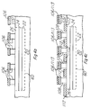
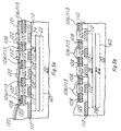
- a second preferred embodiment of the present invention is a method for fabricating high power heterojunction bipolar transistors (HBTs) using the circuit of Figure 3 as a basis and includes the following steps as illustrated in the cross sectional elevation views (taken through axis A-A in Figure 3) of Figures 4A-4E.
- HBTs high power heterojunction bipolar transistors
- a third preferred embodiment fabrication method of the present invention is also directed toward the fabrication of high-power HBTs. This method is identical to the second preferred embodiment method with the exception of different steps (f) and (g) as follows:
- the polyimide layer 120 can either be removed, or left in place as a protective coating.
- a fourth preferred embodiment of the present invention is illustrated in Figure 6 and is directed toward the fabrication of low-power, low-noise HBTs.
- the circuit of Figure 6 contains an emitter disk 30, emitter contact 40, base metallization 50, active area 60 and collector contact 70. These elements are analogous to the like numbered structures in Figure 3. In the low-power, low-noise embodiment, however, only a small emitter disk 30 area is required (for example, one disk 30 is shown in Figure 6).
- the second and third preferred embodiment fabrication techniques can be used to make the device of Figure 6 with no modifications to the process.
- the artwork of the various photoresist masks will determine whether a high-power device or a low-power, low-noise device is formed. In either case, the fabrication process steps are the same.
- the fourth preferred embodiment of the present invention will provide improved low-power, low-noise performance over prior art devices due to the fact that the emitter area does not cross over the implantation edge defining the active area 60, as it does in prior art devices.
- the advantage is achieved because most of the recombination current, which is responsible for increased noise in the device, has been found to be at the edge of the active area 60 (the interface between the implanted and non-implanted areas). If the emitter were to cross this boundary, recombination currents would increase,thereby increasing the noise of the device. Consequently, good low-noise performance is available from devices constructed according to the present invention, as is good high-power performance.
- the same process may be used to construct both types of devices on the same substrate, such as in a monolithic microwave integrated circuit (MMIC), without sacrificing the performance of either device type.
- MMIC monolithic microwave integrated circuit
- Internal and external connections can be ohmic, capacitive, direct or indirect, via intervening circuits or otherwise. Implementation is contemplated in discrete components or fully integrated circuits in silicon, gallium arsenide, or other electronic materials families.
Landscapes
- Bipolar Transistors (AREA)
Applications Claiming Priority (2)
| Application Number | Priority Date | Filing Date | Title |
|---|---|---|---|
| US66209391A | 1991-02-28 | 1991-02-28 | |
| US662093 | 1991-02-28 |
Publications (1)
| Publication Number | Publication Date |
|---|---|
| EP0501279A1 true EP0501279A1 (en) | 1992-09-02 |
Family
ID=24656356
Family Applications (1)
| Application Number | Title | Priority Date | Filing Date |
|---|---|---|---|
| EP92102659A Withdrawn EP0501279A1 (en) | 1991-02-28 | 1992-02-18 | Microwave heterojunction bipolar transistors suitable for low-power, low-noise and high-power applications and method for fabricating same |
Country Status (5)
| Country | Link |
|---|---|
| US (1) | US5528060A (cg-RX-API-DMAC7.html) |
| EP (1) | EP0501279A1 (cg-RX-API-DMAC7.html) |
| JP (1) | JPH07169776A (cg-RX-API-DMAC7.html) |
| KR (1) | KR920017278A (cg-RX-API-DMAC7.html) |
| TW (1) | TW204412B (cg-RX-API-DMAC7.html) |
Cited By (1)
| Publication number | Priority date | Publication date | Assignee | Title |
|---|---|---|---|---|
| US5773353A (en) * | 1994-12-15 | 1998-06-30 | Electronics And Telecommunications Research Institute | Method of fabricating a semiconductor substrate |
Families Citing this family (2)
| Publication number | Priority date | Publication date | Assignee | Title |
|---|---|---|---|---|
| US5761028A (en) * | 1996-05-02 | 1998-06-02 | Chrysler Corporation | Transistor connection assembly having IGBT (X) cross ties |
| CN101189728A (zh) * | 2005-06-01 | 2008-05-28 | Nxp股份有限公司 | 利用改进的npn双极晶体管基极接入电阻的方法和器件 |
Citations (3)
| Publication number | Priority date | Publication date | Assignee | Title |
|---|---|---|---|---|
| FR2309981A1 (fr) * | 1975-04-30 | 1976-11-26 | Sony Corp | Dispositif semi-conducteur comportant une heterojonction |
| FR2352404A1 (fr) * | 1976-05-20 | 1977-12-16 | Comp Generale Electricite | Transistor a heterojonction |
| EP0335720A2 (en) * | 1988-03-30 | 1989-10-04 | Kabushiki Kaisha Toshiba | Bipolar transistor device and method of manufacturing the same |
Family Cites Families (5)
| Publication number | Priority date | Publication date | Assignee | Title |
|---|---|---|---|---|
| US3444443A (en) * | 1966-12-26 | 1969-05-13 | Hitachi Ltd | Semiconductor device for high frequency and high power use |
| KR900001394B1 (en) * | 1985-04-05 | 1990-03-09 | Fujitsu Ltd | Super high frequency intergrated circuit device |
| US5063427A (en) * | 1987-10-13 | 1991-11-05 | Northrop Corporation | Planar bipolar transistors including heterojunction transistors |
| US5097312A (en) * | 1989-02-16 | 1992-03-17 | Texas Instruments Incorporated | Heterojunction bipolar transistor and integration of same with field effect device |
| JP2804095B2 (ja) * | 1989-07-10 | 1998-09-24 | 株式会社東芝 | ヘテロ接合バイボーラトランジスタ |
-
1992
- 1992-02-18 EP EP92102659A patent/EP0501279A1/en not_active Withdrawn
- 1992-02-27 KR KR1019920003077A patent/KR920017278A/ko not_active Ceased
- 1992-02-28 JP JP4043614A patent/JPH07169776A/ja active Pending
- 1992-10-22 TW TW081108412A patent/TW204412B/zh active
-
1994
- 1994-08-17 US US08/291,789 patent/US5528060A/en not_active Expired - Lifetime
Patent Citations (3)
| Publication number | Priority date | Publication date | Assignee | Title |
|---|---|---|---|---|
| FR2309981A1 (fr) * | 1975-04-30 | 1976-11-26 | Sony Corp | Dispositif semi-conducteur comportant une heterojonction |
| FR2352404A1 (fr) * | 1976-05-20 | 1977-12-16 | Comp Generale Electricite | Transistor a heterojonction |
| EP0335720A2 (en) * | 1988-03-30 | 1989-10-04 | Kabushiki Kaisha Toshiba | Bipolar transistor device and method of manufacturing the same |
Non-Patent Citations (2)
| Title |
|---|
| IEEE MTT-S INTERNATIONAL MICROWAVE SYMPOSIUM DIGEST vol. I, 13 June 1989, LONG BEACH USA pages 1061 - 1064; G.W. WANG ET AL.: 'design optimization of microwave power heterojunction bipolar transistor cells' * |
| MICROELECTRONICS JOURNAL vol. 19, no. 5, September 1988, OXFORD GREAT BRITAIN pages 23 - 27; J.K. SINGH ET AL.: 'Air bridge and via hole technology for GaAs based microwave devices' * |
Cited By (1)
| Publication number | Priority date | Publication date | Assignee | Title |
|---|---|---|---|---|
| US5773353A (en) * | 1994-12-15 | 1998-06-30 | Electronics And Telecommunications Research Institute | Method of fabricating a semiconductor substrate |
Also Published As
| Publication number | Publication date |
|---|---|
| US5528060A (en) | 1996-06-18 |
| KR920017278A (ko) | 1992-09-26 |
| TW204412B (cg-RX-API-DMAC7.html) | 1993-04-21 |
| JPH07169776A (ja) | 1995-07-04 |
Similar Documents
| Publication | Publication Date | Title |
|---|---|---|
| EP0747964B1 (en) | Fully self-aligned submicron heterojunction bipolar transistor and method of fabricating the same | |
| US5268315A (en) | Implant-free heterojunction bioplar transistor integrated circuit process | |
| US5512496A (en) | Method of making collector-up bipolar transistor having improved emitter injection efficiency | |
| US5208184A (en) | P-n junction diffusion barrier employing mixed dopants | |
| US5155561A (en) | Permeable base transistor having an electrode configuration for heat dissipation | |
| US6159816A (en) | Method of fabricating a bipolar transistor | |
| JP3248941B2 (ja) | ヘテロ接合バイポーラ・トランジスタをピン・ダイオードと統合する方法 | |
| US6462362B1 (en) | Heterojunction bipolar transistor having prevention layer between base and emitter | |
| US5344786A (en) | Method of fabricating self-aligned heterojunction bipolar transistors | |
| US5270223A (en) | Multiple layer wide bandgap collector structure for bipolar transistors | |
| US5648278A (en) | Method for fabricating microwave heterojunction bipolar transistors suitable for low-power, low-noise and high-power applications | |
| US5171697A (en) | Method of forming multiple layer collector structure for bipolar transistors | |
| US5757039A (en) | Collector up heterojunction bipolar transistor | |
| US20030157777A1 (en) | Method of fabricating self-aligned silicon carbide semiconductor devices | |
| US5528060A (en) | Microwave heterojunction bipolar transistors suitable for low-power, low-noise, and high-power applications | |
| US5332912A (en) | Heterojunction bipolar transistor | |
| KR100296705B1 (ko) | 이종 접합 쌍극자 소자를 이용한 집적 회로 소자의 제조 방법 | |
| US5471078A (en) | Self-aligned heterojunction bipolar transistor | |
| US5073508A (en) | Method of manufacturing an integrated semiconductor circuit including a bipolar heterojunction transistor and/or buried resistors | |
| JP4092597B2 (ja) | 半導体装置及びその製造方法 | |
| JP3235574B2 (ja) | ヘテロバイポーラトランジスタを有する半導体装置の製造方法 | |
| EP0520482A2 (en) | Multiple layer collector structure for bipolar transistors | |
| JP2000124226A (ja) | ヘテロ接合バイポーラトランジスタ及びかかるトランジスタを形成する方法 | |
| JPH06168954A (ja) | 水平コレクタヘテロ接合バイポーラトランジスタおよび形成方法 | |
| JPH0290626A (ja) | 半導体装置の製造方法 |
Legal Events
| Date | Code | Title | Description |
|---|---|---|---|
| PUAI | Public reference made under article 153(3) epc to a published international application that has entered the european phase |
Free format text: ORIGINAL CODE: 0009012 |
|
| AK | Designated contracting states |
Kind code of ref document: A1 Designated state(s): DE FR GB IT NL |
|
| 17P | Request for examination filed |
Effective date: 19930225 |
|
| 17Q | First examination report despatched |
Effective date: 19941214 |
|
| STAA | Information on the status of an ep patent application or granted ep patent |
Free format text: STATUS: THE APPLICATION IS DEEMED TO BE WITHDRAWN |
|
| 18D | Application deemed to be withdrawn |
Effective date: 19970524 |