EP0498457B1 - Dispositif de modulation à bande résiduelle, de type numérique - Google Patents
Dispositif de modulation à bande résiduelle, de type numérique Download PDFInfo
- Publication number
- EP0498457B1 EP0498457B1 EP92102087A EP92102087A EP0498457B1 EP 0498457 B1 EP0498457 B1 EP 0498457B1 EP 92102087 A EP92102087 A EP 92102087A EP 92102087 A EP92102087 A EP 92102087A EP 0498457 B1 EP0498457 B1 EP 0498457B1
- Authority
- EP
- European Patent Office
- Prior art keywords
- output
- component
- multiplier
- frequency
- adder
- Prior art date
- Legal status (The legal status is an assumption and is not a legal conclusion. Google has not performed a legal analysis and makes no representation as to the accuracy of the status listed.)
- Expired - Lifetime
Links
Images


Classifications
-
- H—ELECTRICITY
- H04—ELECTRIC COMMUNICATION TECHNIQUE
- H04L—TRANSMISSION OF DIGITAL INFORMATION, e.g. TELEGRAPHIC COMMUNICATION
- H04L27/00—Modulated-carrier systems
- H04L27/02—Amplitude-modulated carrier systems, e.g. using on-off keying; Single sideband or vestigial sideband modulation
- H04L27/04—Modulator circuits; Transmitter circuits
Definitions
- the present invention relates to a digital type VSB modulation apparatus for generating a VSB (vestigial sideband) modulation signal from a digital baseband signal.
- a video modulation means used in a conventional television transmission apparatus AM-modulates an analog baseband signal to convert it into a DSB (double sideband) modulation signal, and limits the bandwidth of the DSB modulation signal using a band-pass filter included in an intermediate frequency circuit or a transmission frequency circuit, thereby obtaining a VSB modulation signal (see, e.g., "Broadcast Technology Library 10, Broadcast Equipment, Chapter 3, Television Broadcast Equipment” issued on April 20, 1983 by Nippon Hoso Publishing Inc.).
- the band-pass filter a surface acoustic filter is generally used as the band-pass filter.
- the surface acoustic filter is economically disadvantageous since separate filters must be prepared in units of use frequencies.
- the surface acoustic filter suffers from large ripples of group delay time characteristics due to its structure. For this reason, the group delay time characteristics of a transmission apparatus itself depend on the surface acoustic filter.
- Document FR-A-2 633 127 discloses a numerical method and an apparatus for VSB modulation comprising a signal processor as complex filter means. Furthermore, a SSB generator is known from document EP-A-0 323 675 to provide a digitized SSB signal having a desired carrier frequency. In this generator, a digitized analog signal is processed in accordance with Weavers method.
- the present invention has been made in consideration of the above situation, and has as its object to provide a digital type VSB modulation apparatus, which can generate a VSB modulation signal from a digital baseband signal with a simple arrangement.
- a digital type VSB modulation apparatus comprising: generation means having filter means for extracting a low-frequency component from a digitalized baseband signal, delay means for executing a delay process of delaying the baseband signal for a period of time corresponding to a processing time of the filter means, and subtracter means for obtaining a high-frequency component of the baseband signal by subtracting a low-frequency component extracted by the filter means from an output of the delay means, for generating an in-phase component of a modulation signal having a frequency spectrum having a high-frequency component whose level is a half of that of a low-frequency component thereof, and an orthogonal component of the modulation signal of a high-frequency component having a frequency spectrum whose level is a half of that of the low-frequency component; carrier wave component generation means for multiplying the in-phase component and the orthogonal component output from the generation means by carrier wave signals in order to obtain a carrier wave in-phase component and a carrier wave orthogonal component;
- Fig. 1A shows the frequency spectrum of a VSB modulation signal.
- DSB double sideband modulation
- SSB modulation single sideband modulation
- the first term of the right-hand side of equation (1) corresponds to the DSB modulation signal, and the second term thereof corresponds to the SSB modulation signal.
- Fig. 1B shows the frequency spectrum of the DSB modulation signal
- Fig. 1C shows the frequency spectrum of the SSB modulation signal.
- the first term of the right-hand side of equation (2) represents a carrier in-phase component, and the second term thereof represents a carrier orthogonal component.
- Fig. 1D shows the frequency spectrum of the carrier in-phase component
- Fig. 1E shows the frequency spectrum of the carrier orthogonal component.
- a synthesized spectrum of the carrier in-phase component and the carrier orthogonal components becomes the frequency spectrum of the VSB modulation signal shown in Fig. 1.
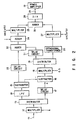
- reference numeral 11 denotes an input terminal, which is supplied with a baseband signal digital-converted at a sampling frequency fs.
- the sampling frequency fs satisfies relations fs > 2f H and fs > 2fc.
- the digital baseband signal supplied to the input terminal 11 is multiplied with the modulation index k by a multiplier 12 so as to be converted to a frequency spectrum shown in Fig. 3A. Thereafter, the baseband signal is supplied to a distributor 13.
- One output of the distributor 13 is supplied to an LPF (low-pass filter) 14, so that the high-frequency components of the baseband signal are cut, thereby extracting low-frequency components falling within a range between 0 and f L Hz, as shown in Fig. 3B.
- the output from the LPF 14 is distributed to two outputs by a distributor 15, and one output is supplied to the negative input terminal "-" of a subtracter 16.
- the other output from the distributor 13 is delayed by a processing time of the LPF 14 by a delay circuit 17, and the delayed output is supplied to the positive input terminal "+" of the subtracter 16.
- the subtracter 16 subtracts the low-frequency components of the baseband signal (Fig. 3B) supplied to its negative input terminal "-" from the original baseband signal (Fig. 3A) supplied to its positive input terminal "+”, thereby extracting high-frequency components of the baseband signal falling within a range between f L and f H Hz, as shown in Fig. 3C.
- the high-frequency baseband signal output from the subtracter 16 is multiplied with a fixed coefficient "0.5" by a multiplier 18 so as to be converted into a frequency spectrum shown in Fig. 3D. Thereafter, the baseband signal is supplied to a distributor 19.
- One output from the distributor 19 is supplied to an orthogonal transformer 20.
- the orthogonal transformer 20 has a function, known as the Hilbert transformation, of shifting the phase of a signal in the entire target frequency band through 90°. More specifically, if the input to the orthogonal transformer 20 is given by: (k/2) ⁇ cos2 ⁇ f 2 ⁇ t then, the transformer transforms its output to: -(k/2) ⁇ sin2 ⁇ f 2 ⁇ t
- the other output from the distributor 19, which output is given by: (k/2) ⁇ cos2 ⁇ f 2 ⁇ t is delayed by a processing time of the orthogonal transformer 20 by a delay circuit 23, and the delayed output is supplied to one input terminal of an adder 22.
- the other output from the distributor 15, which output is given by: k ⁇ cos2 ⁇ f 1 ⁇ t is delayed by a processing time of the orthogonal transformer 20 by a delay circuit 23, and the delayed output is supplied to the other input terminal of the adder 22.
- the adder 22 adds the low-frequency baseband signal shown in Fig. 3B to the high-frequency baseband signal shown in Fig. 3D, thereby generating a baseband signal having a frequency spectrum shown in Fig. 3E.
- the output from the adder 22 is added to a constant "1" by an adder 24, and the sum output is multiplied, by a multiplier 25, with a carrier component given by: cos2 ⁇ fc ⁇ t
- a carrier in-phase component shown in Fig. 4A i.e., the first term of the right-hand side of equation (2) described above, is obtained, and is supplied to one input terminal of an adder 26.
- the output from the orthogonal transformer 20, which output is given by: -(k/2) ⁇ sin2 ⁇ f 2 ⁇ t is multiplied, by a multiplier 27, with the carrier component given by: sin2 ⁇ fc ⁇ t
- a carrier orthogonal component shown in Fig. 4B i.e., the second term of the right-hand side of equation (2) described above is obtained, and is supplied to the other input terminal of the adder 26.
- cos2 ⁇ fc ⁇ t and sin2 ⁇ fc ⁇ t the spectrum levels at two sides of a carrier become half the spectrum level of the original baseband signal.
- the adder 26 adds the carrier in-phase component and the carrier orthogonal component shown in Figs. 4A and 4B, thereby generating a VSB modulation signal having a frequency spectrum shown in Fig. 4C. Thereafter, the VSB modulation signal output from the adder 26 is converted into an analog signal by a D/A (digital-to-analog) converter 28, and is output through an output terminal 29. The VSB modulation signal is then supplied to a power amplifier 10 for, e.g., transmission.
- the carrier in-phase component and the carrier orthogonal component are generated from a digital baseband signal, and these components are added to each other to obtain the VSB modulation signal, the arrangement can become very simple and compact as compared with the prior art wherein circuit sections are simply replaced with digital circuits having the same functions.
- FIG. 2 exemplifies a case wherein the condition fs > 2fc is satisfied.
- Fig. 5 shows a modification when this condition is not satisfied.
- the same reference numerals in Fig. 5 denote the same parts as in Fig. 2.
- interpolators 30 and 31 are respectively inserted between the adder 24 and the multiplier 25, and between the orthogonal transformer 20 and the multiplier 27. These interpolators 30 and 31 have a function of converting the sampling frequency fs to a frequency corresponding to an integer multiple of the frequency fs while preserving the spectrum of an input signal.
- an output sampling frequency fs 1 of the interpolators 30 and 31 is set to satisfy: fs1 > 2fc the above embodiment can also be applied to a case wherein the carrier frequency fc is high, and the sampling frequency fs of the baseband signal is lower than a frequency twice the carrier frequency fc.
- Fig. 6 shows another modification of the embodiment shown in Fig. 2.
- the outputs from the adder 24 and the orthogonal transformer 20 are converted into analog signals respectively through D/A (digital-to-analog) converters 32 and 33.
- the multipliers 25 and 27 and the adder 26 after the D/A converters 32 and 33 are constituted by analog circuits, and the D/A converter 28 after the adder 26 is omitted.
- the multipliers 25 and 27 and the adder 26 have a function equivalent to that in digital processing, and the adder 26 can output a VSB modulation signal given by equation (2) described above.
- the analog multipliers 25 and 27 can be easily realized by balanced modulators, and the analog adder 26 can be easily realized by a resistor mixing circuit, a transformer, or the like, thus simplifying the arrangement.
- Fig. 7 shows the second embodiment of the present invention. More specifically, reference numeral 34 denotes an input terminal, which is supplied with a baseband signal digital-converted at a sampling frequency fs.
- the sampling frequency fs satisfies relations fs > 2f H and fs > 2fc.
- the digital baseband signal supplied to the input terminal 34 is multiplied with a modulation index k/2 by a multiplier 35, and is then supplied to a distributor 36.
- One output from the distributor 36 is supplied to an LPF 37, so that the high-frequency component of the baseband signal are cut, thereby extracting low-frequency components falling within a range between 0 and f L Hz.
- the output from the LPF 37 is distributed to two outputs by a distributor 38, and one output is supplied to the negative input terminal "-" of a subtracter 39.
- the other output from the distributor 36 is delayed by a processing time of the LPF 37 by a delay circuit 40, and the delayed output is distributed to two outputs by a distributor 41.
- One output from the distributor 41 is supplied to the positive input terminal "+" of the subtracter 39.
- the subtracter 39 subtracts the low-frequency components of the baseband signal from the original baseband signal supplied to its positive input terminal "+", thereby extracting high-frequency components of the baseband signal falling within a range between f L and f H Hz.
- the high-frequency baseband signal output from the subtracter 39 is supplied to an orthogonal transformer 42.
- the orthogonal transformer 42 has a function, known as, e.g., the Hilbert transformation, of shifting the phase of a signal in the entire target frequency band through 90°. More specifically, if the input to the orthogonal transformer 20 is given by: (k/2) ⁇ cos2 ⁇ f 2 ⁇ t then, the transformer transforms its output to: -(k/2) ⁇ sin2 ⁇ f 2 ⁇ t
- the other outputs from the distributors 38 and 41 are added by an adder 43, thus generating a baseband signal having the frequency spectrum previously shown in Fig. 3E.
- the baseband signal is delayed by a processing time of the orthogonal transformer 42 by a delay circuit 44, and the delayed signal is added to a constant "1" by an adder 45. Thereafter, the sum signal is multiplied, by a multiplier 46, with a carrier component given by: cos2 ⁇ fc ⁇ t
- a carrier in-phase component shown in Fig. 4A i.e., the first term of the right-hand side of equation (2) described above is obtained, and is supplied to one input terminal of an adder 47.
- the output from the orthogonal transformer 42 which output is given by: -(k/2) ⁇ sin2 ⁇ f 2 ⁇ t is multiplied, by a multiplier 48, with a carrier component given by: sin2 ⁇ fc ⁇ t
- a carrier orthogonal component shown in Fig. 4B i.e., the second term of the right-hand side of equation (2) described above, is obtained, and is supplied to the other input terminal of the adder 47.
- the adder 47 adds the carrier in-phase component and the carrier orthogonal component shown in Figs. 4A and 4B, thereby generating a VSB modulation signal having a frequency spectrum shown in Fig. 4C. Thereafter, the VSB modulation signal output from the adder 47 is converted into an analog signal by a D/A converter 49, and is output through an output terminal 50. The VSB modulation signal is supplied to a power amplifier for transmission.
- the carrier in-phase component and the carrier orthogonal component are generated from a digital baseband signal, and these components are added to each other to obtain the VSB modulation signal, the arrangement can become very simple and compact as compared with the prior art wherein circuit sections are simply replaced with digital circuits having the same functions.
- FIG. 7 exemplifies a case wherein the condition fs > 2fc is satisfied.
- Fig. 8 shows a modification when this condition is not satisfied.
- the same reference numerals in Fig. 8 denote the same parts as in Fig. 7.
- interpolators 51 and 52 are respectively inserted between the adder 45 and the multiplier 46, and between the orthogonal transformer 42 and the multiplier 48. These interpolators 51 and 52 have a function of converting the sampling frequency fs to a frequency corresponding to an integer multiple of the frequency fs while preserving the spectrum of an input signal.
- an output sampling frequency fs 1 of the interpolators 51 and 52 is set to satisfy: fs1 > 2fc the above embodiment can also be applied to a case wherein the carrier frequency fc is high, and the sampling frequency fs of the baseband signal is lower than a frequency twice the carrier frequency fc.
- Fig. 9 shows another modification of the second embodiment shown in Fig. 7.
- the outputs from the adder 45 and the orthogonal transformer 42 are converted into analog signals respectively through D/A converters 53 and 54.
- the multipliers 46 and 48 and the adder 47 after the D/A converters 53 and 54 are constituted by analog circuits, and the D/A converter 49 after the adder 47 is omitted.
- the multipliers 46 and 48 and the adder 47 have a function equivalent to that in digital processing, and the adder 47 can output a VSB modulation signal given by equation (2) described above.
- the analog multipliers 46 and 48 can be easily realized by balanced modulators, and the analog adder 47 can be easily realized by a resistor mixing circuit, a transformer, or the like, thus simplifying the arrangement.
- the low-frequency components are extracted from the original baseband signal by cutting the high-frequency components, and the extracted low-frequency components are subtracted from the original baseband signal, thereby obtaining the high-frequency components.
- the baseband signal In order to separate the baseband signal into low- and high-frequency components, it can be passed through low- and high-pass filters.
- the VSB modulation signal generated like in each of the above embodiments is amplified by the power amplifier 10.
Landscapes
- Engineering & Computer Science (AREA)
- Computer Networks & Wireless Communication (AREA)
- Signal Processing (AREA)
- Amplitude Modulation (AREA)
Claims (9)
- Dispositif de modulation VSB du type numérique comprenant :caractérisé en ce que le moyen de génération (11 à 22 ; 34 à 44) comprend en outre :un moyen de génération (11 à 22 ; 34 à 44) ayantun moyen de filtre (14 ; 37) pour extraire une composante basse fréquence d'un signal de bande de base numérisé,le moyen de génération fournissant une composante en phase et une composante orthogonale d'un signal de modulation ;un moyen de génération de composante d'onde de porteuse (24, 25, 27 ; 45, 46, 48) pour multiplier la composante en phase et la composante orthogonale fournie par ledit moyen de génération (11 à 22, 34 à 44) par des signaux d'onde de porteuse afin d'obtenir une composante en phase d'onde de porteuse et une composante orthogonale d'onde de porteuse ; etun moyen de synthèse (26, 47) pour synthétiser la composante en phase d'onde de porteuse et la composante orthogonale d'onde de porteuse fournie par ledit moyen de génération de composante d'onde de porteuse (24, 25, 27 ; 45, 46, 48) afin d'obtenir un signal de modulation VSB,un moyen à retard (17 ; 40) pour exécuter un traitement de retard pour retarder ledit signal de bande de base pendant une période de temps correspondant à un temps de traitement dudit moyen de filtre (14 ; 37), etun moyen de soustracteur (16 ; 39) pour obtenir une composante haute fréquence du signal de bande de base en soustrayant une composante basse fréquence extraite par ledit moyen de filtre (14 ; 37) à partir d'une sortie dudit moyen à retard (17 ; 40), pour générer la composante en phase du signal de modulation ayant un spectre de fréquence ayant une composante haute fréquence dont le niveau est la moitié de celui de la composante basse fréquence de celui-ci, et la composante orthogonale de modulation d'une composante haute fréquence ayant un spectre de fréquence dont le niveau est la moitié de celui de la composante haute fréquence.
- Appareil selon la revendication 1 caractérisé en ce que ledit moyen de génération (11 à 22) comprend :un premier moyen de multiplieur (12) pour multiplier le signal de bande de base par un indice de modulation prédéterminé : un moyen de filtre (14) pour extraire une composante basse fréquence d'une sortie dudit premier moyen de multiplieur (12) ; un moyen à retard (14) pour exécuter un traitement de retard pour retarder ledit signal de bande de base pendant une période de temps correspondant à un temps de traitement dudit moyen de filtre (14) ;un moyen de soustracteur (16) pour obtenir une composante haute fréquence du signal de bande de base en soustrayant une sortie dudit moyen de filtre (14) à partir d'une sortie dudit moyen à retard (17) ; un second moyen de multiplieur (18) pour multiplier un niveau de sortie dudit premier moyen de soustracteur (16) par 1/2 ; un moyen de transformation orthogonale (20) pour exécuter un traitement de transformation orthogonale d'une sortie dudit second moyen de multiplieur (18) pour obtenir la composante orthogonale, et un premier moyen d'additionneur (22) pour additionner une sortie dudit second moyen de multiplieur (18) et une sortie dudit moyen de filtre (14) pour obtenir la composante en phase.
- Appareil selon la revendication 2, caractérisée en ce que ledit moyen de génération de composante de porteuse (24, 25, 27) comprend : un second moyen d'additionneur (24) pour additionner une sortie du type premier moyen d'additionneur (22) à une constante 1 ; un troisième moyen de multiplieur (25) pour multiplier une sortie dudit second moyen d'additionneur (24) avec un signal de porteuse ; et un quatrième moyen de multiplieur (27) pour multiplier une sortie dudit moyen de transformateur orthogonal (20) avec un signal de porteuse ayant un déphasage de 90° par rapport au signal de porteuse multiplié par ledit troisième moyen de multiplieur (25).
- Appareil selon la revendication 3, caractérisé en ce qu'il comprend en outre : des interpolateurs (30, 31), insérés entre ledit second moyen d'additionneur (24) et ledit troisième moyen de multiplieur (25), et entre ledit moyen de transformateur orthogonal (20) et ledit quatrième moyen de multiplieur (27), pour convertir une fréquence d'échantillonnage afin de générer le signal de modulation VSB même lorsque la fréquence d'échantillonnage du signal de bande de base est inférieure à une fréquence double de la fréquence de porteuse.
- Appareil selon la revendication 3, caractérisé en ce qu'il comprend en outre : un moyen de convertisseur numérique analogique (32, 33), disposé entre ledit second moyen d'additionneur (24) et ledit troisième moyen d'additionneur (25), et entre ledit moyen de transformateur orthogonal (20) et ledit quatrième moyen de multiplieur (27), de sorte que ledit troisième moyen de multiplieur (25), ledit quatrième moyen de multiplieur (27), et ledit moyen de synthèse (26) sont constitués par des circuits analogiques.
- Appareil selon la revendication 1, caractérisé en ce que ledit moyen de génération (34 à 44) comprend : un premier moyen de multiplieur (35) pour multiplier le signal de bande de base par un indice de modulation prédéterminé ; un moyen de filtre (37) pour extraire une composante basse fréquence d'une sortie dudit premier moyen de multiplier (35); un moyen à retard (40) pour exécuter un traitement de retard pour retarder ledit signal de bande de base pendant une période de temps correspondant à un temps de traitement dudit moyen de filtre (37) ; un moyen de soustracteur (39) pour obtenir une composante haute fréquence du signal de bande de base en soustrayant une sortie dudit moyen de filtre (37) d'une sortie dudit moyen à retard (40) ; un moyen de transformateur orthogonal (42) pour exécuter un traitement de transformation orthogonale d'une sortie dudit moyen de soustracteur (39) pour obtenir la composante orthogonale ; et un premier moyen d'additionneur (43) pour additionner une sortie dudit moyen à retard (40) et une sortie dudit moyen de filtre (37) pour obtenir la composante en phase.
- Appareil selon la revendication 6, caractérisé en ce que ledit moyen de génération de composante de porteuse (45, 46, 48) comprend : un second moyen d'additionneur (45) pour additionner une sortie dudit premier moyen d'additionneur (43) à une constante 1 ; un second moyen de multiplieur (46) pour multiplier une sortie dudit second moyen d'additionneur (45) avec un signal de porteuse ; et un troisième moyen de multiplieur (48) pour multiplier une sortie dudit moyen de transformateur orthogonal (42) avec un signal de porteuse ayant un déphasage de 90° par rapport au signal de porteuse multiplié par ledit second moyen de multiplieur (46).
- Appareil selon la revendication 7, caractérisé en ce qu'il comprend en outre : des interpolateurs (51, 52), insérés entre ledit second moyen d'additionneur (45) et ledit second moyen de multiplieur (46), et entre ledit moyen de transformateur orthogonal (42) et ledit troisième moyen de multiplieur (48), pour convertir une fréquence d'échantillonnage afin de générer le signal de modulation VSB même lorsque la fréquence d'échantillonnage du signal de bande de base est inférieure à une fréquence double d'une fréquence de porteuse.
- Appareil selon la revendication 7, caractérisé en ce qu'il comprend en outre : un moyen de convertisseur numérique-analogique (53, 54) disposé entre ledit second moyen d'additionneur (45) et ledit second moyen de multiplieur (46), et entre ledit moyen de transformateur orthogonal (42) et ledit troisième moyen de multiplieur (48), pour que ledit second moyen de multiplieur (46), ledit troisième moyen de multiplieur (48), et ledit moyen de synthèse (47) soient constitués par des circuits analogiques.
Applications Claiming Priority (4)
| Application Number | Priority Date | Filing Date | Title |
|---|---|---|---|
| JP18030/91 | 1991-02-08 | ||
| JP1803091 | 1991-02-08 | ||
| JP208200/91 | 1991-08-20 | ||
| JP03208200A JP3086723B2 (ja) | 1991-02-08 | 1991-08-20 | デジタル型vsb変調装置 |
Publications (3)
| Publication Number | Publication Date |
|---|---|
| EP0498457A2 EP0498457A2 (fr) | 1992-08-12 |
| EP0498457A3 EP0498457A3 (en) | 1993-09-15 |
| EP0498457B1 true EP0498457B1 (fr) | 1999-05-06 |
Family
ID=26354643
Family Applications (1)
| Application Number | Title | Priority Date | Filing Date |
|---|---|---|---|
| EP92102087A Expired - Lifetime EP0498457B1 (fr) | 1991-02-08 | 1992-02-07 | Dispositif de modulation à bande résiduelle, de type numérique |
Country Status (3)
| Country | Link |
|---|---|
| US (1) | US5327462A (fr) |
| EP (1) | EP0498457B1 (fr) |
| JP (1) | JP3086723B2 (fr) |
Families Citing this family (8)
| Publication number | Priority date | Publication date | Assignee | Title |
|---|---|---|---|---|
| EP0617531A1 (fr) * | 1993-03-25 | 1994-09-28 | Matsushita Electric Industrial Co., Ltd. | Système de transmission multirésolution |
| US5596606A (en) * | 1994-04-05 | 1997-01-21 | Scientific-Atlanta, Inc. | Synchronous detector and methods for synchronous detection |
| US5764701A (en) * | 1996-03-04 | 1998-06-09 | Zenith Electronics Corporation | VSB modulator |
| US5801595A (en) * | 1997-01-10 | 1998-09-01 | Harris Corporation | Device and method for digital vestigial sideband modulation |
| US5946047A (en) * | 1997-03-12 | 1999-08-31 | Hybrid Networks, Inc. | Network system for handling digital data over a TV channel |
| US5946048A (en) * | 1997-03-12 | 1999-08-31 | Hybrid Networks, Inc. | Network device for handling digital data over a TV channel |
| JPH1168696A (ja) * | 1997-08-19 | 1999-03-09 | Sony Corp | 通信方法及び送信装置及び受信装置並びにセルラー無線通信システム |
| JP2006311353A (ja) * | 2005-04-28 | 2006-11-09 | Samsung Electronics Co Ltd | ダウンコンバータおよびアップコンバータ |
Family Cites Families (4)
| Publication number | Priority date | Publication date | Assignee | Title |
|---|---|---|---|---|
| DE1165104B (de) * | 1959-06-16 | 1964-03-12 | Fernseh Gmbh | Verfahren und Anordnung zur weitgehenden Kompensation der bei der Restseitenbanduebertragung auftretenden Signalfehler |
| GB1166153A (en) * | 1967-06-30 | 1969-10-08 | Standard Telephones Cables Ltd | Signal Transmission System |
| GB2214374A (en) * | 1988-01-06 | 1989-08-31 | Philips Electronic Associated | Ssb signal generator |
| FR2633127A1 (fr) * | 1988-06-17 | 1989-12-22 | Trt Telecom Radio Electr | Procede de modulation d'un signal en bande laterale unique et modulateur par lequel est mis en oeuvre le procede |
-
1991
- 1991-08-20 JP JP03208200A patent/JP3086723B2/ja not_active Expired - Lifetime
-
1992
- 1992-02-07 US US07/832,724 patent/US5327462A/en not_active Expired - Lifetime
- 1992-02-07 EP EP92102087A patent/EP0498457B1/fr not_active Expired - Lifetime
Also Published As
| Publication number | Publication date |
|---|---|
| US5327462A (en) | 1994-07-05 |
| EP0498457A3 (en) | 1993-09-15 |
| JP3086723B2 (ja) | 2000-09-11 |
| JPH04297112A (ja) | 1992-10-21 |
| EP0498457A2 (fr) | 1992-08-12 |
Similar Documents
| Publication | Publication Date | Title |
|---|---|---|
| US4974236A (en) | Arrangement for generating an SSB signal | |
| US4799214A (en) | Two-wire full duplex frequency division multiplex modem system having echo cancellation means | |
| EP0676880A2 (fr) | Modulateur/démodulateur avec filtrage en bande de base | |
| KR20000052914A (ko) | 전송방법 및 그 방법의 실행을 위한 장치 | |
| EP0498457B1 (fr) | Dispositif de modulation à bande résiduelle, de type numérique | |
| JPH01231575A (ja) | ゴースト除去装置 | |
| KR100957426B1 (ko) | 무선기 | |
| US5682431A (en) | FM stereo broadcasting apparatus and method | |
| KR960014117B1 (ko) | 신호 분리 장치 | |
| JP2918857B2 (ja) | デジタルセンターラインフィルタ | |
| KR950013627B1 (ko) | 고스트 제거 회로 | |
| US8379740B2 (en) | Wide-band signal processor | |
| EP0623269B1 (fr) | Echantillonnage de signal | |
| JP2991509B2 (ja) | デジタル型vsb変調装置 | |
| US6920471B2 (en) | Compensation scheme for reducing delay in a digital impedance matching circuit to improve return loss | |
| EP1160978A1 (fr) | Filtre numérique | |
| EP0970563B1 (fr) | Filtre a temps discret | |
| KR100550629B1 (ko) | 피드포워드 방식을 이용하여 스퓨리어스 특성을 개선하기위한직접 디지털 주파수 합성 장치 및 그 방법 | |
| US7139326B2 (en) | Image-canceling quadrature modulator and method | |
| JPH06311134A (ja) | 直交周波数分割多重信号発生器 | |
| KR100745770B1 (ko) | 복소 계수 트랜스버설 필터 및 이것을 적용한 무선 통신시스템 | |
| US7705760B2 (en) | Method and device for the filtering and analogue/digital conversion of analogue signal | |
| Udalov | Digital Hilbert transformer for single-sideband generation | |
| JPH06120990A (ja) | 直交変調回路 | |
| JP2705363B2 (ja) | 自動干渉除去装置 |
Legal Events
| Date | Code | Title | Description |
|---|---|---|---|
| PUAI | Public reference made under article 153(3) epc to a published international application that has entered the european phase |
Free format text: ORIGINAL CODE: 0009012 |
|
| 17P | Request for examination filed |
Effective date: 19920304 |
|
| AK | Designated contracting states |
Kind code of ref document: A2 Designated state(s): FR GB |
|
| PUAL | Search report despatched |
Free format text: ORIGINAL CODE: 0009013 |
|
| AK | Designated contracting states |
Kind code of ref document: A3 Designated state(s): FR GB |
|
| 17Q | First examination report despatched |
Effective date: 19960905 |
|
| GRAG | Despatch of communication of intention to grant |
Free format text: ORIGINAL CODE: EPIDOS AGRA |
|
| GRAG | Despatch of communication of intention to grant |
Free format text: ORIGINAL CODE: EPIDOS AGRA |
|
| GRAH | Despatch of communication of intention to grant a patent |
Free format text: ORIGINAL CODE: EPIDOS IGRA |
|
| GRAH | Despatch of communication of intention to grant a patent |
Free format text: ORIGINAL CODE: EPIDOS IGRA |
|
| GRAA | (expected) grant |
Free format text: ORIGINAL CODE: 0009210 |
|
| AK | Designated contracting states |
Kind code of ref document: B1 Designated state(s): FR GB |
|
| ET | Fr: translation filed | ||
| PLBE | No opposition filed within time limit |
Free format text: ORIGINAL CODE: 0009261 |
|
| STAA | Information on the status of an ep patent application or granted ep patent |
Free format text: STATUS: NO OPPOSITION FILED WITHIN TIME LIMIT |
|
| 26N | No opposition filed | ||
| REG | Reference to a national code |
Ref country code: GB Ref legal event code: IF02 |
|
| PGFP | Annual fee paid to national office [announced via postgrant information from national office to epo] |
Ref country code: FR Payment date: 20110120 Year of fee payment: 20 |
|
| PGFP | Annual fee paid to national office [announced via postgrant information from national office to epo] |
Ref country code: GB Payment date: 20110209 Year of fee payment: 20 |
|
| REG | Reference to a national code |
Ref country code: GB Ref legal event code: PE20 Expiry date: 20120206 |
|
| PG25 | Lapsed in a contracting state [announced via postgrant information from national office to epo] |
Ref country code: GB Free format text: LAPSE BECAUSE OF EXPIRATION OF PROTECTION Effective date: 20120206 |