EP0492548B1 - Méthode pour réduire un bruit de phase introduit par une resynchronisation de signaux numériques à l'aide de justification et circuits intégrés pour la mise en oeuvre d'une telle méthode - Google Patents
Méthode pour réduire un bruit de phase introduit par une resynchronisation de signaux numériques à l'aide de justification et circuits intégrés pour la mise en oeuvre d'une telle méthode Download PDFInfo
- Publication number
- EP0492548B1 EP0492548B1 EP91122022A EP91122022A EP0492548B1 EP 0492548 B1 EP0492548 B1 EP 0492548B1 EP 91122022 A EP91122022 A EP 91122022A EP 91122022 A EP91122022 A EP 91122022A EP 0492548 B1 EP0492548 B1 EP 0492548B1
- Authority
- EP
- European Patent Office
- Prior art keywords
- block
- signal
- clock signal
- local
- justification
- Prior art date
- Legal status (The legal status is an assumption and is not a legal conclusion. Google has not performed a legal analysis and makes no representation as to the accuracy of the status listed.)
- Expired - Lifetime
Links
Images


Classifications
-
- H—ELECTRICITY
- H04—ELECTRIC COMMUNICATION TECHNIQUE
- H04J—MULTIPLEX COMMUNICATION
- H04J3/00—Time-division multiplex systems
- H04J3/02—Details
- H04J3/06—Synchronising arrangements
- H04J3/07—Synchronising arrangements using pulse stuffing for systems with different or fluctuating information rates or bit rates
- H04J3/076—Bit and byte stuffing, e.g. SDH/PDH desynchronisers, bit-leaking
Definitions
- the present invention relates to a method for reducing a phase noise introduced in a resynchronisation by justification of digital signals used in the data and/or voice transmission, and a device for the implementation of such a method.
- the justification method is widely used for desynchronising a plesiochronous stream, characterised by using a local clock.
- An international standard (CITT, e.g. recommendations G707 - G709 for the multiplexers of the synchronous hierarchy) establishes the characteristics of tributary streams, the characteristics of aggregated streams, the structures of frames and the position and the number of justification digits for each level of the consolidated multiplexing hierarchies.
- the traditional structure of a resynchronizer using justification includes an elastic memory into which data is written with the clock rate associated to the plesiochronous stream and from which data read out by the local clock, to which is appended a frame that includes digits of the so-called justification or filling.
- justification method Three types of the justification method can be distinguished: positive, negative or positive-negative justification, according to whether the filling digits are normally used as information, not usually used as information, or both types of justification digits are present in each frame.
- justification digits is established once for each frame, based on the comparison between the digital signal representing the phase difference between the local and remote clock and one (in case of positive or negative justification) or two (in case of positive-negative justification) fixed thresholds.
- phase noise is particularly high when the filling factor reaches values near to a rational number p/q, where p and q are integer positive numbers.
- the international standard establishes the limits related to the phase noise present in the desynchronized stream (CCITT, e.g. recomm. G783 for the synchronous multiplexers) and, in case of plesiochronous multiplexers, it establishes the frame structures so that these limits have to be respected when operating the justification by the above mentioned conventional method.
- the drawback is that the reduction value is limited by the presence of "peaks" in the phase noise obtained after the desynchronization towards the detuning of the plesiochronous stream with respect to the nominal frequency value.
- Figure 1 refers the result of a simulation made for the case of a plesiochronous tributary at 2,048 Mb/sec mapped by the positive-negative justification in a VC-12 ("Virtual Container with level 1,2") of a frame STM-1.
- the ordinates indicate the peak-peak amplitude App of the phase noise or jitter, obtained in response of the desynchronization made by PLL, while the abscisses refer the detuning D freq between the real frequency of the plesiochronous flow and the nominal frequency, normalized at the frame frequency.
- a phase comparison signal between a local clock signal and a remote clock signal is obtained, said phase comparison signal is modified by a suitable scale factor, the modified phase comparison signal is integrated with a suitable frequency, the integrated signal is quantised with a suitable pitch, and the justification events which are to be overlapped to a local unjustified clock signal are determined in conjunction with the transitions of the quantised signal and with the justification opportunities relating to the used frame format.
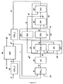
- Figure 2 shows a block b1 (COMP) representing the phase comparison function between a remote clock signal s1, coming from a far source (not shown) and associated with a data stream to be resynchronized, and a local justified clock signal s7.
- COMP block b1
- a block processing b1 is a signal having a phase difference s2, which is multiplied in a block b2 (MOLT) by a constant K1, thus generating a signal s3.
- a block b3 (INT) carries out the integration of the signal s3 at a clock frequency s10 and generates an integrated signal s4, which is compared with the thresholds, assumed to be infinite, of an ideal quantizer (block b4, QUANT), K being the separation between the thresholds.
- the output of a block b4 is a signal s5 quantized with step K, whose transitions, sampled at a clock frequency s11, generate the justification events in a block b5 (JUST); these events are overlapped at prefixed time periods to a local clock signal s6 for generating the resynchronized clock signal for the justification s7.
- the described structure is a discrete, nonlinear and sampled control system since the justification events can occur only in prefixed time periods.
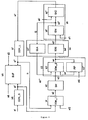
- FIG. 3 A possible implementation of the method, using a completely digital technique, is shown in Figure 3, wherein an elastic memory (block b8, BUF) works as an interface between data (s8) associated to the remote clock signal s1 and data (s9) resynchronized by the justification with the local clock signal s7.
- an elastic memory block b8, BUF
- the reference symbol s1' indicates the numerical value, encoded in binary system as a complement to 2, of the phase associated to the writing clock of the elastic memory, generated by a writing counter controlled by s1 (block b6, CON_S) and s7' that is the similar signal related to the reading clock generated by a reading counter controlled by s7 (block b7, CON_L).
- the reading and writing phases are compared in the block b1 (SOM_1), which is a digital adder (as a complement to 2), and added to a constant polarization value s12, whose value depends on the mean frequency of the unjustified clock signal s6 and the dimension of the memory b8.
- SOM_1 is a digital adder (as a complement to 2)
- the resulting digital signal s2 is multiplied by a constant coefficient K1, dimensioned as a power of 2 and therefore can be realized by a shifter (block b2, SHI), generating the digital signal s3.
- This signal is applied to a digital storage b3, formed by blocks b3' (SOM_2) and b3" (PIP), to a digital adder (as a complement to 2) and to a register of the "parallel input - parallel output” type.
- the register is clocked at frequency s10; according to the described embodiment this clock rate is associated to the reading of the elastic memory (that is the clock signal on which the counter b7 (CON_L) evolves).
- this clock rate is associated to the reading of the elastic memory (that is the clock signal on which the counter b7 (CON_L) evolves).
- any frequency value under the Shannon's theorem relatively to the signal s7' sampling is suitable.
- the cumulated value s4 is quantized with step K in the block b4, which is formed by a circuit with one or two thresholds (b4', SOG), by a feedback line 12 and a gain block b4" (GUA).
- step K is formed by a circuit with one or two thresholds (b4', SOG), by a feedback line 12 and a gain block b4" (GUA).
- a block b4' includes a threshold in the case the system must apply the decisions related to purely positive or negative justifications, and two thresholds in the case the system must apply the decisions related to both of justification types.
- the result of the comparison with a thresholds s5' is applied to the justifier b5, formed by a pulse generator b5' (GIM) and by a suppressor/adder of clock pulses b5" (SAD).
- GEM pulse generator
- SAD suppressor/adder of clock pulses b5"
- the block b5' generates pulses in conjunction with the shootings of thresholds of b4', with positive or negative polarity according to the sign of exceeded threshold.
- the operation frequency of the device is s11, which is equal to the maximum possible frequency allowed for the evolution of justification events.
- a polarized pulse series s5" on one side is applied by the line 12 to the gain block b4", on the other side causes in the block b5" the overlapping of positive or negative justifications according to the sign of pulses, the local clock signal s6, generating the resynchronized clock rate for the justification s7.
- the line 12 and the block b4" establish a value K at the input of the accumulator b3, in conjunction with each justification event, and having a sign depending on the sign of the introduced justification.
- the reading counter b7 of the elastic memory reconstructs s7', which is applied again to the block b1 of phase comparison, causing the closing of the feeback loop.
- Figure 4 represents a variant of the scheme of Figure 3, in which a circuit having one sole threshold (block b4', SOG) is used also for the case of a frame characterized by positive-negative justification.
- the local unjustified clock signal s6 is formed by a signal s6' on which rigidly preestablished justifyings of determined polarity are overlapped at suitable frequency.
- the invention accomplishes the sole justifications of polarity opposite to the preestablished polarities, necessary and sufficient to reach the resynchronization.
- f I K1/K ⁇ D f CAMP f CAMP being the value of the frequency associated to the clock s10.
- a system of this type has a low-pass characteristic with respect to a signal sent in input towards the phase comparator, and a high-pass characteristic with respect to a signal sent to output towards the controlled oscillator.
- phase resynchronization noise is an effect of the quantization related to the justification process, it can be considered a signal sent into the feedback loop to the output of the block b5, and then to the output of controlled oscillator.
- the device carries out an operation of high-pass filtering onto the resynchronization phase noise with a notch frequency given by the equation (4), and therefore it can be suitably sized by the selection of the coefficients K and K1 for each operation condition related to the frequency of the incoming plesiochronous flow and to the type of used justification.
- This filtering allows to eliminate the components of low frequency of phase noise; the components of the high frequency components are automatically cut by the PLL, that makes the desynchronization in reception.
Landscapes
- Engineering & Computer Science (AREA)
- Computer Networks & Wireless Communication (AREA)
- Signal Processing (AREA)
- Synchronisation In Digital Transmission Systems (AREA)
- Time-Division Multiplex Systems (AREA)
- Stabilization Of Oscillater, Synchronisation, Frequency Synthesizers (AREA)
- Semiconductor Integrated Circuits (AREA)
- Digital Transmission Methods That Use Modulated Carrier Waves (AREA)
Claims (10)
- Procédé pour réduire un bruit de phase introduit pendant la resynchronisation par justification de signaux numériques utilisés en transmission de données et/ou de paroles, comportant les étapes consistant à :obtenir un signal (s2) de comparaison de phase entre un signal d'horloge local justifié (s7) et un signal d'horloge distant (s1) ;modifier par un facteur d'échelle approprié le signal (s2) de comparaison de phase ;intégrer avec une fréquence appropriée le signal de comparaison de phase modifié (s3) ;quantifier le signal intégré (s4) ; etdéterminer les événements de justification qui doivent être superposés à un signal d'horloge local non justifié (s6) en conjonction avec les transitions du signal quantifié (s5) pour générer ledit signal d'horloge local justifié (s7).
- Procédé selon la revendication 1, dans lequel le facteur d'échelle, la fréquence pour l'intégration et l'étape de quantification sont sélectionnés en fonction de la largeur de bande de transmission.
- Procédé selon la revendication 1 ou 2, dans lequel des justifications sont établies dans une direction ou dans l'autre direction selon que le signal intégré (s4) a un comportement d'augmentation ou de diminution.
- Procédé selon l'une quelconque des revendications 1 à 3, dans lequel un cas de justification positive-négative est réduit à un cas de justification purement positive ou négative en introduisant dans le signal d'horloge local non justifié (S6) des justifications préétablies à polarité prédéterminée avec une fréquence appropriée.
- Dispositif pour réduire un bruit de phase introduit pendant la resynchronisation par justification de signaux numériques utilisés en transmission de données et/ou de paroles, comprenant :un moyen (bloc b1) pour générer un signal (s2) de comparaison de phase entre un signal d'horloge justifié (s7) et un signal d'horloge distant (s1) ;un moyen (bloc b2) pour modifier par un facteur d'échelle approprié le signal de comparaison (s2) ;un moyen (bloc b3) pour intégrer avec une fréquence appropriée le signal de comparaison de phase modifié (s3) ;un moyen (bloc b4) pour quantifier le signal intégré (s4) ; etun moyen (bloc b5) pour générer le signal d'horloge local justifié (s7) en utilisant des transitions du signal quantifié (s5) pour déterminer quels événements de justification doivent être superposés à un signal d'horloge local non justifié (s6) pour générer ledit signal d'horloge local justifié (s7).
- Dispositif selon la revendication 5, dans lequel ledit moyen (bloc 1) pour générer un signal de comparaison de phase comprend un additionneur numérique, ledit moyen (bloc b2) pour modifier le signal de comparaison comprenant un système de déplacement numérique, ledit moyen d'intégration (bloc b3) comprend un additionneur numérique (bloc b3') et un registre à entrée parallèle/sortie parallèle (bloc b3"), ledit moyen de quantification (bloc b4) comprend un comparateur avec un ou deux seuils (bloc b4'), et ledit moyen (bloc b5) pour générer le signal d'horloge local justifié comprend un générateur d'impulsions (bloc b5') et un suppresseur/additionneur de signaux d'horloge (bloc b5") de signaux d'horloge.
- Dispositif selon la revendication 6, comportant en outre une mémoire élastique constituée par une mémoire tampon (bloc b8), un compteur d'écriture (bloc b6) et un compteur de lecture (bloc b7), ladite mémoire élastique servant d'interface entre les données associées au signal d'horloge distant (si) et les données associées au signal d'horloge local justifié (s7).
- Dispositif selon la revendication 7, dans lequel le moyen (bloc b1) pour générer un signal de comparaison de phase effectue la génération du signal (s2) de comparaison de phase sous une forme numérique par soustraction binaire comme complément à 2 de données issues des compteurs d'écriture et de lecture de la mémoire élastique.
- Dispositif selon la revendication 7 ou 8, dans lequel le moyen (bloc b1) pour générer un signal de comparaison de phase ajoute une constante (s12) au signal (s2) de comparaison de phase, ladite constante étant basée sur la dimension de la mémoire élastique et la fréquence principale du signal d'horloge local non justifié (s6).
- Dispositif selon l'une quelconque des revendications 6 à 9, dans lequel ledit moyen de quantification (bloc b4) comporte un bloc de gain (bloc b4"), ledit moyen (bloc 5) pour générer le signal d'horloge local justifié comporte en outre un générateur d'impulsions (bloc b5'), ledit bloc de gain et ledit générateur d'impulsions étant reliés par une ligne de retour (ligne 12) de façon que, compte tenu dudit circuit de comparaison à un ou deux seuils, un quantificateur à seuils infinis soit réalisé.
Applications Claiming Priority (2)
| Application Number | Priority Date | Filing Date | Title |
|---|---|---|---|
| IT02249690A IT1244350B (it) | 1990-12-21 | 1990-12-21 | Metodo per la riduzione del rumore di fase introdotto nella resincronizzazione di segnali digitali mediante giustificazione, e circuiti integrati per l'implementazione del metodo |
| IT2249690 | 1990-12-21 |
Publications (3)
| Publication Number | Publication Date |
|---|---|
| EP0492548A2 EP0492548A2 (fr) | 1992-07-01 |
| EP0492548A3 EP0492548A3 (en) | 1993-03-10 |
| EP0492548B1 true EP0492548B1 (fr) | 1997-03-05 |
Family
ID=11197057
Family Applications (1)
| Application Number | Title | Priority Date | Filing Date |
|---|---|---|---|
| EP91122022A Expired - Lifetime EP0492548B1 (fr) | 1990-12-21 | 1991-12-20 | Méthode pour réduire un bruit de phase introduit par une resynchronisation de signaux numériques à l'aide de justification et circuits intégrés pour la mise en oeuvre d'une telle méthode |
Country Status (6)
| Country | Link |
|---|---|
| US (1) | US5276715A (fr) |
| EP (1) | EP0492548B1 (fr) |
| JP (1) | JP3273511B2 (fr) |
| DE (1) | DE69124957T2 (fr) |
| ES (1) | ES2097784T3 (fr) |
| IT (1) | IT1244350B (fr) |
Families Citing this family (3)
| Publication number | Priority date | Publication date | Assignee | Title |
|---|---|---|---|---|
| DE4303356A1 (de) * | 1993-02-05 | 1994-08-11 | Philips Patentverwaltung | Digitale Phasenregelschleife |
| GB9323187D0 (en) * | 1993-11-10 | 1994-01-05 | Northern Telecom Ltd | Pointer justification even leak control |
| ES2102938B1 (es) * | 1994-03-28 | 1998-04-16 | Alcatel Standard Electrica | Sistema de reduccion de fluctuaciones de fase en demultiplexores digitales. |
Family Cites Families (6)
| Publication number | Priority date | Publication date | Assignee | Title |
|---|---|---|---|---|
| US4019153A (en) * | 1974-10-07 | 1977-04-19 | The Charles Stark Draper Laboratory, Inc. | Digital phase-locked loop filter |
| FR2450008A1 (fr) * | 1979-02-21 | 1980-09-19 | Portejoie Jean Francois | Circuit de synchronisation de signaux numeriques plesiochrones par justification |
| DE3315372A1 (de) * | 1983-04-28 | 1984-10-31 | Philips Patentverwaltung Gmbh, 2000 Hamburg | Anordnung zur umsetzung eines anisochronen binaeren eingangssignales in ein isochrones binaeres ausgangssignal |
| CA1262173A (fr) * | 1986-05-29 | 1989-10-03 | James Angus Mceachern | Synchronisation de signaux de donnees asynchrones |
| US5052025A (en) * | 1990-08-24 | 1991-09-24 | At&T Bell Laboratories | Synchronous digital signal to asynchronous digital signal desynchronizer |
| US5036294A (en) * | 1990-12-03 | 1991-07-30 | Motorola Inc. | Phase locked loop having low-frequency jitter compensation |
-
1990
- 1990-12-21 IT IT02249690A patent/IT1244350B/it active IP Right Grant
-
1991
- 1991-12-19 US US07/810,672 patent/US5276715A/en not_active Expired - Lifetime
- 1991-12-20 JP JP35505091A patent/JP3273511B2/ja not_active Expired - Fee Related
- 1991-12-20 EP EP91122022A patent/EP0492548B1/fr not_active Expired - Lifetime
- 1991-12-20 ES ES91122022T patent/ES2097784T3/es not_active Expired - Lifetime
- 1991-12-20 DE DE69124957T patent/DE69124957T2/de not_active Expired - Lifetime
Also Published As
| Publication number | Publication date |
|---|---|
| DE69124957D1 (de) | 1997-04-10 |
| ES2097784T3 (es) | 1997-04-16 |
| IT9022496A1 (it) | 1992-06-21 |
| IT9022496A0 (it) | 1990-12-21 |
| EP0492548A2 (fr) | 1992-07-01 |
| EP0492548A3 (en) | 1993-03-10 |
| IT1244350B (it) | 1994-07-08 |
| JPH0563689A (ja) | 1993-03-12 |
| DE69124957T2 (de) | 1997-09-25 |
| JP3273511B2 (ja) | 2002-04-08 |
| US5276715A (en) | 1994-01-04 |
Similar Documents
| Publication | Publication Date | Title |
|---|---|---|
| US5526362A (en) | Control of receiver station timing for time-stamped data | |
| EP0473338B1 (fr) | Synchronisation de bit à mémoire élastique | |
| US6252850B1 (en) | Adaptive digital clock recovery | |
| JP3092352B2 (ja) | Sonetをds−n信号に対して非同期化する装置及び方法 | |
| US5404380A (en) | Desynchronizer for adjusting the read data rate of payload data received over a digital communication network transmitting payload data within frames | |
| US6088413A (en) | Apparatus for reducing jitter in a desynchronizer | |
| US5796796A (en) | Pointer adjustment jitter cancellation processor utilizing phase hopping and phase leaking techniques | |
| US5276688A (en) | Circuit arrangement for bit rate adjustment | |
| WO1993016536A1 (fr) | Desynchronisateur et procede pour supprimer le sautillement de l'indicateur dans un desynchronisateur | |
| EP0876017A1 (fr) | Système numérique de récupération d'horloge | |
| US5282206A (en) | Synchronization circuit for establishing frame synchronism using pointers in a digital transmission system | |
| TW529250B (en) | NCO based frequency synthesizer with jitter modulation | |
| EP0492548B1 (fr) | Méthode pour réduire un bruit de phase introduit par une resynchronisation de signaux numériques à l'aide de justification et circuits intégrés pour la mise en oeuvre d'une telle méthode | |
| CA2472691C (fr) | Traitement numerique des pointeurs sonet | |
| JPH07177113A (ja) | 伝送装置及び整合用回路 | |
| US5703915A (en) | Transmission system and multiplexing/demultiplexing equipment involving a justifiable bit stream | |
| US7440533B2 (en) | Modulated jitter attenuation filter | |
| US5774509A (en) | Method for the reduction of phase noise introduced by the SDH network (Synchronous Digital Hierarchy Network) by pointer justification and integrated circuits for the implementation of the method | |
| EP0842573B1 (fr) | Desynchronisateur de signaux video emis | |
| EP0492549B1 (fr) | Méthode pour réduire le bruit de phase introduit dans un réseau de type SDH utilisant une justification par pointeurs, et circuits integrés propres à une mise en oeuvre de cette méthode | |
| WO1993016535A1 (fr) | Procede de suppression du sautillement de l'indicateur dans un desynchronisateur | |
| JPH07226760A (ja) | ポインタ調整イベント漏れ制御方法および装置 | |
| US5937021A (en) | Digital phase-locked loop for clock recovery | |
| JP3140285B2 (ja) | データレート変換装置 | |
| JPH0923220A (ja) | クロック信号回復用の回路、制御ループ及びそれらからなる送信システム |
Legal Events
| Date | Code | Title | Description |
|---|---|---|---|
| PUAI | Public reference made under article 153(3) epc to a published international application that has entered the european phase |
Free format text: ORIGINAL CODE: 0009012 |
|
| AK | Designated contracting states |
Kind code of ref document: A2 Designated state(s): BE CH DE ES FR GB LI NL SE |
|
| PUAL | Search report despatched |
Free format text: ORIGINAL CODE: 0009013 |
|
| AK | Designated contracting states |
Kind code of ref document: A3 Designated state(s): BE CH DE ES FR GB LI NL SE |
|
| K1C3 | Correction of patent application (complete document) published |
Effective date: 19920701 |
|
| 17P | Request for examination filed |
Effective date: 19930824 |
|
| 17Q | First examination report despatched |
Effective date: 19950612 |
|
| GRAG | Despatch of communication of intention to grant |
Free format text: ORIGINAL CODE: EPIDOS AGRA |
|
| GRAH | Despatch of communication of intention to grant a patent |
Free format text: ORIGINAL CODE: EPIDOS IGRA |
|
| RAP1 | Party data changed (applicant data changed or rights of an application transferred) |
Owner name: ALCATEL ITALIA S.P.A. |
|
| GRAH | Despatch of communication of intention to grant a patent |
Free format text: ORIGINAL CODE: EPIDOS IGRA |
|
| GRAA | (expected) grant |
Free format text: ORIGINAL CODE: 0009210 |
|
| AK | Designated contracting states |
Kind code of ref document: B1 Designated state(s): BE CH DE ES FR GB LI NL SE |
|
| REG | Reference to a national code |
Ref country code: CH Ref legal event code: NV Representative=s name: TROESCH SCHEIDEGGER WERNER AG Ref country code: CH Ref legal event code: EP |
|
| REF | Corresponds to: |
Ref document number: 69124957 Country of ref document: DE Date of ref document: 19970410 |
|
| REG | Reference to a national code |
Ref country code: ES Ref legal event code: FG2A Ref document number: 2097784 Country of ref document: ES Kind code of ref document: T3 |
|
| ET | Fr: translation filed | ||
| PLBE | No opposition filed within time limit |
Free format text: ORIGINAL CODE: 0009261 |
|
| STAA | Information on the status of an ep patent application or granted ep patent |
Free format text: STATUS: NO OPPOSITION FILED WITHIN TIME LIMIT |
|
| 26N | No opposition filed | ||
| PGFP | Annual fee paid to national office [announced via postgrant information from national office to epo] |
Ref country code: CH Payment date: 19991115 Year of fee payment: 9 |
|
| PGFP | Annual fee paid to national office [announced via postgrant information from national office to epo] |
Ref country code: NL Payment date: 19991122 Year of fee payment: 9 |
|
| PGFP | Annual fee paid to national office [announced via postgrant information from national office to epo] |
Ref country code: BE Payment date: 19991216 Year of fee payment: 9 |
|
| PG25 | Lapsed in a contracting state [announced via postgrant information from national office to epo] |
Ref country code: LI Free format text: LAPSE BECAUSE OF NON-PAYMENT OF DUE FEES Effective date: 20001231 Ref country code: BE Free format text: LAPSE BECAUSE OF NON-PAYMENT OF DUE FEES Effective date: 20001231 Ref country code: CH Free format text: LAPSE BECAUSE OF NON-PAYMENT OF DUE FEES Effective date: 20001231 |
|
| BERE | Be: lapsed |
Owner name: ALCATEL ITALIA S.P.A. Effective date: 20001231 |
|
| PG25 | Lapsed in a contracting state [announced via postgrant information from national office to epo] |
Ref country code: NL Free format text: LAPSE BECAUSE OF NON-PAYMENT OF DUE FEES Effective date: 20010701 |
|
| REG | Reference to a national code |
Ref country code: CH Ref legal event code: PL |
|
| NLV4 | Nl: lapsed or anulled due to non-payment of the annual fee |
Effective date: 20010701 |
|
| PGFP | Annual fee paid to national office [announced via postgrant information from national office to epo] |
Ref country code: SE Payment date: 20011203 Year of fee payment: 11 |
|
| PGFP | Annual fee paid to national office [announced via postgrant information from national office to epo] |
Ref country code: ES Payment date: 20011212 Year of fee payment: 11 |
|
| REG | Reference to a national code |
Ref country code: GB Ref legal event code: IF02 |
|
| PG25 | Lapsed in a contracting state [announced via postgrant information from national office to epo] |
Ref country code: SE Free format text: LAPSE BECAUSE OF NON-PAYMENT OF DUE FEES Effective date: 20021221 Ref country code: ES Free format text: LAPSE BECAUSE OF NON-PAYMENT OF DUE FEES Effective date: 20021221 |
|
| EUG | Se: european patent has lapsed | ||
| REG | Reference to a national code |
Ref country code: ES Ref legal event code: FD2A Effective date: 20021221 |
|
| PGFP | Annual fee paid to national office [announced via postgrant information from national office to epo] |
Ref country code: FR Payment date: 20100108 Year of fee payment: 19 Ref country code: GB Payment date: 20091218 Year of fee payment: 19 |
|
| PGFP | Annual fee paid to national office [announced via postgrant information from national office to epo] |
Ref country code: DE Payment date: 20091222 Year of fee payment: 19 |
|
| GBPC | Gb: european patent ceased through non-payment of renewal fee |
Effective date: 20101220 |
|
| REG | Reference to a national code |
Ref country code: FR Ref legal event code: ST Effective date: 20110831 |
|
| PG25 | Lapsed in a contracting state [announced via postgrant information from national office to epo] |
Ref country code: FR Free format text: LAPSE BECAUSE OF NON-PAYMENT OF DUE FEES Effective date: 20110103 |
|
| REG | Reference to a national code |
Ref country code: DE Ref legal event code: R119 Ref document number: 69124957 Country of ref document: DE Effective date: 20110701 |
|
| PG25 | Lapsed in a contracting state [announced via postgrant information from national office to epo] |
Ref country code: GB Free format text: LAPSE BECAUSE OF NON-PAYMENT OF DUE FEES Effective date: 20101220 Ref country code: DE Free format text: LAPSE BECAUSE OF NON-PAYMENT OF DUE FEES Effective date: 20110701 |