EP0488802A2 - An active matrix display device - Google Patents
An active matrix display device Download PDFInfo
- Publication number
- EP0488802A2 EP0488802A2 EP91311143A EP91311143A EP0488802A2 EP 0488802 A2 EP0488802 A2 EP 0488802A2 EP 91311143 A EP91311143 A EP 91311143A EP 91311143 A EP91311143 A EP 91311143A EP 0488802 A2 EP0488802 A2 EP 0488802A2
- Authority
- EP
- European Patent Office
- Prior art keywords
- buses
- active matrix
- group
- feedlines
- matrix display
- Prior art date
- Legal status (The legal status is an assumption and is not a legal conclusion. Google has not performed a legal analysis and makes no representation as to the accuracy of the status listed.)
- Granted
Links
Images


Classifications
-
- G—PHYSICS
- G02—OPTICS
- G02F—OPTICAL DEVICES OR ARRANGEMENTS FOR THE CONTROL OF LIGHT BY MODIFICATION OF THE OPTICAL PROPERTIES OF THE MEDIA OF THE ELEMENTS INVOLVED THEREIN; NON-LINEAR OPTICS; FREQUENCY-CHANGING OF LIGHT; OPTICAL LOGIC ELEMENTS; OPTICAL ANALOGUE/DIGITAL CONVERTERS
- G02F1/00—Devices or arrangements for the control of the intensity, colour, phase, polarisation or direction of light arriving from an independent light source, e.g. switching, gating or modulating; Non-linear optics
- G02F1/01—Devices or arrangements for the control of the intensity, colour, phase, polarisation or direction of light arriving from an independent light source, e.g. switching, gating or modulating; Non-linear optics for the control of the intensity, phase, polarisation or colour
- G02F1/13—Devices or arrangements for the control of the intensity, colour, phase, polarisation or direction of light arriving from an independent light source, e.g. switching, gating or modulating; Non-linear optics for the control of the intensity, phase, polarisation or colour based on liquid crystals, e.g. single liquid crystal display cells
- G02F1/133—Constructional arrangements; Operation of liquid crystal cells; Circuit arrangements
- G02F1/136—Liquid crystal cells structurally associated with a semi-conducting layer or substrate, e.g. cells forming part of an integrated circuit
- G02F1/1362—Active matrix addressed cells
- G02F1/136286—Wiring, e.g. gate line, drain line
Definitions
- the present invention relates to a display device which displays by impressing drive signals on pixel electrodes used for display through switching elements, and more particularly to a display device which can perform a high density display by arranging pixel electrodes in a matrix.
- a liquid crystal display device, an EL display device and a plasma display device are known in the art in which pixel electrodes are selected and driven so as to display desired patterns on a screen.
- the display medium sealed between the electrodes is optically modulated by impressing a voltage between the selected pixel electrodes and the respective counter electrodes. The optical modulation is visually observed.
- An active matrix driving method is known as a driving method of pixel electrode. The active matrix driving method will be described as follows:
- Pixel electrodes are independently arranged, and then provided with switching elements.
- the pixel electrodes are driven through the switching elements.
- TFTs thin film transistor
- MIMs metal-insulating layer-metal
- MOS transistors diodes
- varistors varistors and other known devices
- This type of active matrix method enables the display device to have a good contrast in the picture, and finds many applications such as in television, word processors, and display panels of computer terminals.
- buses are likely to be formed with the possibility of breakage during the fabrication of switching elements, buses, pixel electrodes on the active matrix substrate.
- a possible breakage of buses is detected as a line defect on the screen.
- the line defect is fatal for the display device.
- Defective display devices must be discarded, thereby decreasing production yield of display devices.
- Figure 6 shows an active matrix display which is driven by TFTs 31.
- the active matrix has a structure made by two layers in which a conductive film wiring 23 is stacked on source buses 22 which cross over gate buses 21.
- This active matrix has a dual structure which includes conductive film wiring 23 arranged on the source buses 22. This dual structure is obtained by leaving the transparent conductive film on the source buses 22 after the source buses 22 are formed in pattern, when pixel electrodes 41 are formed with a transparent conductive film.
- the source buses 22 and the conductive film wirings 23 pass portions stepped by the gate buses at the junctions of the gate buses 21 and the source buses 22, so that the source buses 22 and a conductive film wiring 23 are likely to break. This is caused by the fact that the source buses 22 and the conductive film wiring 23 do not fully cover the stepped portions made by the gate buses 21, and that the source buses 22 and the conductive film wiring 23 are separated owing to poor adhesion of the insulating films to the gate buses 21. The problem of breakage is nevertheless not solved by the dual structure.
- the etchant is likely to erode the metal parts of the source buses 22.
- the source buses 22 are liable to breakage.
- the active matrix display device of the present invention which overcomes the above-discussed and numerous other disadvantages and deficiencies of the prior art, comprises a pair of insulating substrates, a first group of buses formed on one of the sides of the insulating substrates, a second group of buses crossing the first group of buses, conductive film wirings formed on the second group of buses, wherein the width of each conductive film wiring at stepped portions of the first group of buses is not smaller than that of the conductive film wirings located out of the stepped portions.
- the active matrix display device further comprises an additional capacitance for maintaining charges stored in the pixel electrode, and an additional capacitance wiring located opposite to the pixel electrode.
- the active matrix display device further comprises a first layer of a-Si(i) and a second layer of SiNx both held between the first group of buses and the second group of buses.
- the two additional layers are formed in pattern.
- the invention described herein makes possible the objective of providing an active matrix display device which can maintain electric connection even in the case where the second group of buses are broken, thereby maintaining high production yield.
- the active matrix substrate includes the gate buses 21 in parallel with each other, the source buses 22 crossing the gate buses, and the conductive film wiring 23.
- the substrate 1 also includes gate bus branch lines 25 branched from the gate buses 21.
- the TFTs 31 are formed on the gate electrode 25.
- the conductive film wiring 23 have a larger width on the stepped portions of the gate buses 21 than parts thereof located out of the stepped portions.
- a metal layer is deposited on the glass substrate by sputtering, and then it is formed into the gate buses 21 and the gate bus branch lines 25 by patterning.
- the metal layer instead of Ta, Ti, Al or Cr can be used, wherein the metal layer can be made as a single layer or a multi-layer. If necessary, the whole surface of the glass substrate can be coated with a base film of Ta2O5 or any other suitable metal oxides before the gate buses 21 are formed.
- the gate insulation film 11 is formed on the gate buses 21 by depositing SiNx as a film having a thickness of 300 nm by a plasma CVD method.
- the surfaces of the gate buses 21 and the gate bus branch line 25 can be anode-oxidized so as to enhance the insulating ability of the gate buses 21 and the gate bus branch lines 25.
- a-Si(i) an intrinsic semiconductor amorphous silicon
- SiNx layer which functions as an etching stopper 13
- the a-Si(i) layer has a thickness of 30 nm and the SiNx layer has a thickness of 200 nm.
- a layer of amorphous silicon of n+ type containing P (phosphorus) hereinafter called a-Si(n+)
- a-Si(n+) which eventually becomes a contact layer 14 is deposited on the two layers by a CVD method.
- the a-Si(n+) layer has a thickness of 80 nm.
- the semiconductor layer 12 and the contact layer 14 are formed by patterning the a-Si(n+) layer and the a-Si(i) layer.
- the contact layer 14 provides ohmic contact between the semiconductor layer 12 and the source electrode 32 and the drain electrode 33, both of which are formed at a later stage.
- the source buses 22, the source electrode 32 and drain electrode 33 are formed by depositing a Ti metal layer over the whole substrate 1 and then patterning it.
- a Ti metal layer instead of Ti, for example, Al, Mo, and Cr can be used for the metal layer.
- each conductive film wiring 23 is not narrower than the source bus 22, and is overlaid on it.
- the width of each conductive film wiring 23 at the stepped portion is not smaller than the width thereof located out of the stepped portions.
- a protective layer 17 of SiNx is formed over the whole surface of the substrate 1.
- the protective layer 17 can be a window-open type; that is, the protective layer 17 is partly removed in a central portion of the pixel electrode.
- an orientation film 19 can be formed on the protective layer 17.
- a counter substrate facing the active matrix substrate is fabricated with a counter electrode 3 and substrate is fabricated with a counter electrode 3 and an orientation film 9 on a substrate 2.
- a liquid crystal layer 18 is placed and sealed between the counter electrode 3 and the substrate 1. In this way, the active matrix display device is fabricated.
- the conductive film wiring 23 over any stepped portions at the junctions where the conductive film wiring 23 and the gate buses 21 cross each other has a relatively great width so that even if the source buses 22 break at the stepped portion, the broken source bus or buses can maintain an electric connection because of a lessened degree of breakage.
- This active matrix display device contains an additional capacitance 51 to hold charges stored in the pixel electrode.
- the additional capacitance 51 is formed between the pixel electrode 41 and an additional capacitance wiring 42.
- the additional capacitance wiring 42 is formed at the same time as when the gate buses 21 are formed.
- the additional capacitance wiring 42 is located opposite to the pixel electrode 41 with the gate insulating film 11 sandwiched therebetween. The same signal is applied to the counter electrode 3 and the additional capacitance wiring 42. Therefore the additional capacitance 51 and a pixel capacitance formed by the pixel electrode 41 and the counter electrode 3 become parallel.
- the conductive film wiring 23 is relatively wider over the stepped portions at the junctions where the conductive film wiring 23 and the gate buses 21 cross each other.
- the conductive film wirings 23 are relatively wide at the stepped portions at the junctions where the gate buses 21 and the additional capacitance wiring 42 cross each other.
- the additional capacitance wiring 42 prevents breakage of the conductive film wiring 23.
- an a-Si(i) layer 44 and a SiNx layer 43 are held between the gate buses 21 and source buses 22.
- the a-Si(i) layer 44 and the SiNx layer 43 are pattern-formed at the same time as when the semiconductor layer 12 and etching stopper 13 are formed.
- the insulating ability is enhanced between the gate buses 21 and source buses 22.
- the conductive film wiring 23 at the stepped portions caused by the gate buses 21 has a width greater than the other parts thereof located out of the stepped portions.
- the conductive film wirings 23 are protected against breakage or at least they are less liable to breakage. Even if the source buses 22 breaks at the stepped portions, the electrical connection is advantageously maintained.
- these layers can be made of the same materials as that for the contact layer 14.
- the active matrix substrates of the present invention find many applications such as in display devices using an MIM, an MOS, a transistor, a diode or a varistor as a switching element.
Landscapes
- Physics & Mathematics (AREA)
- Nonlinear Science (AREA)
- Mathematical Physics (AREA)
- Chemical & Material Sciences (AREA)
- Crystallography & Structural Chemistry (AREA)
- General Physics & Mathematics (AREA)
- Optics & Photonics (AREA)
- Engineering & Computer Science (AREA)
- Microelectronics & Electronic Packaging (AREA)
- Liquid Crystal (AREA)
- Thin Film Transistor (AREA)
- Devices For Indicating Variable Information By Combining Individual Elements (AREA)
Abstract
Description
- The present invention relates to a display device which displays by impressing drive signals on pixel electrodes used for display through switching elements, and more particularly to a display device which can perform a high density display by arranging pixel electrodes in a matrix.
- A liquid crystal display device, an EL display device and a plasma display device are known in the art in which pixel electrodes are selected and driven so as to display desired patterns on a screen. The display medium sealed between the electrodes is optically modulated by impressing a voltage between the selected pixel electrodes and the respective counter electrodes. The optical modulation is visually observed. An active matrix driving method is known as a driving method of pixel electrode. The active matrix driving method will be described as follows:
- Pixel electrodes are independently arranged, and then provided with switching elements. The pixel electrodes are driven through the switching elements. TFTs (thin film transistor), MIMs (metal-insulating layer-metal), MOS transistors, diodes, varistors and other known devices are known as switching elements which select and drive the pixel electrodes. This type of active matrix method enables the display device to have a good contrast in the picture, and finds many applications such as in television, word processors, and display panels of computer terminals.
- In the known active matrix display devices, buses are likely to be formed with the possibility of breakage during the fabrication of switching elements, buses, pixel electrodes on the active matrix substrate. A possible breakage of buses is detected as a line defect on the screen. The line defect is fatal for the display device. Defective display devices must be discarded, thereby decreasing production yield of display devices.
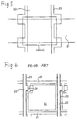
- In order to solve these problems mentioned above, various proposals have been made. One example is shown in Figure 6. Figure 6 shows an active matrix display which is driven by
TFTs 31. The active matrix has a structure made by two layers in which aconductive film wiring 23 is stacked onsource buses 22 which cross overgate buses 21. This active matrix has a dual structure which includesconductive film wiring 23 arranged on thesource buses 22. This dual structure is obtained by leaving the transparent conductive film on thesource buses 22 after thesource buses 22 are formed in pattern, whenpixel electrodes 41 are formed with a transparent conductive film. - However, in the dual structure described above, the
source buses 22 and theconductive film wirings 23 pass portions stepped by the gate buses at the junctions of thegate buses 21 and thesource buses 22, so that thesource buses 22 and aconductive film wiring 23 are likely to break. This is caused by the fact that thesource buses 22 and theconductive film wiring 23 do not fully cover the stepped portions made by thegate buses 21, and that thesource buses 22 and theconductive film wiring 23 are separated owing to poor adhesion of the insulating films to thegate buses 21. The problem of breakage is nevertheless not solved by the dual structure. - In addition, when the
source buses 22 are fabricated by etching, the etchant is likely to erode the metal parts of thesource buses 22. Thesource buses 22 are liable to breakage. - The active matrix display device of the present invention, which overcomes the above-discussed and numerous other disadvantages and deficiencies of the prior art, comprises a pair of insulating substrates, a first group of buses formed on one of the sides of the insulating substrates, a second group of buses crossing the first group of buses, conductive film wirings formed on the second group of buses, wherein the width of each conductive film wiring at stepped portions of the first group of buses is not smaller than that of the conductive film wirings located out of the stepped portions.
- In a preferred embodiment, the active matrix display device, further comprises an additional capacitance for maintaining charges stored in the pixel electrode, and an additional capacitance wiring located opposite to the pixel electrode.
- In a preferred embodiment, the active matrix display device further comprises a first layer of a-Si(i) and a second layer of SiNx both held between the first group of buses and the second group of buses.
- In a preferred embodiment, the two additional layers are formed in pattern.
- Thus, the invention described herein makes possible the objective of providing an active matrix display device which can maintain electric connection even in the case where the second group of buses are broken, thereby maintaining high production yield.
- This invention may be better understood and its numerous objects and advantages will become apparent to those skilled in the art by reference to the accompanying drawings as follows:
- Figure 1 is a plan view showing an active matrix substrate used in a first example of an active matrix display device according to the present invention;
- Figure 2 is a plan view on an enlarged scale showing portions where gate buses and source buses in Figure 1 cross;
- Figure 3 is a sectional view taken along the line p-p in Figure 1;
- Figure 4 is a plan view showing an active matrix substrate used in another example of the present invention;
- Figure 5 is a plan view on an enlarged scale showing junctions where gate buses and source buses of the active matrix substrate used a third example according to the present invention cross; and
- Figure 6 is a plan view showing a conventional active matrix substrate.
- Referring to Figures 1 to 3, a first example of the invention will be described:
- The active matrix substrate includes the
gate buses 21 in parallel with each other, thesource buses 22 crossing the gate buses, and theconductive film wiring 23. Thesubstrate 1 also includes gatebus branch lines 25 branched from thegate buses 21. TheTFTs 31 are formed on thegate electrode 25. - As shown in Figure 2, which shows a junction where the gate buses 21 and the
source bus 22 cross each other, theconductive film wiring 23 have a larger width on the stepped portions of thegate buses 21 than parts thereof located out of the stepped portions. - The process of fabricating the active matrix substrate will be described:
- A metal layer is deposited on the glass substrate by sputtering, and then it is formed into the
gate buses 21 and the gatebus branch lines 25 by patterning. To form the metal layer, instead of Ta, Ti, Al or Cr can be used, wherein the metal layer can be made as a single layer or a multi-layer. If necessary, the whole surface of the glass substrate can be coated with a base film of Ta₂O₅ or any other suitable metal oxides before thegate buses 21 are formed. - Next, the
gate insulation film 11 is formed on thegate buses 21 by depositing SiNx as a film having a thickness of 300 nm by a plasma CVD method. Before thegate insulation film 11 is formed, the surfaces of thegate buses 21 and the gatebus branch line 25 can be anode-oxidized so as to enhance the insulating ability of thegate buses 21 and the gatebus branch lines 25. - The next step is that an intrinsic semiconductor amorphous silicon (hereinafter called "a-Si(i)") layer, which eventually becomes a
semiconductor layer 12, and a SiNx layer, which functions as anetching stopper 13, are successively deposited by a plasma CVD method. The a-Si(i) layer has a thickness of 30 nm and the SiNx layer has a thickness of 200 nm. In addition, a layer of amorphous silicon of n⁺ type containing P (phosphorus) (hereinafter called a-Si(n⁺)), which eventually becomes acontact layer 14, is deposited on the two layers by a CVD method. The a-Si(n⁺) layer has a thickness of 80 nm. Thesemiconductor layer 12 and thecontact layer 14 are formed by patterning the a-Si(n⁺) layer and the a-Si(i) layer. Thecontact layer 14 provides ohmic contact between thesemiconductor layer 12 and thesource electrode 32 and thedrain electrode 33, both of which are formed at a later stage. - Then, the
source buses 22, thesource electrode 32 anddrain electrode 33 are formed by depositing a Ti metal layer over thewhole substrate 1 and then patterning it. Instead of Ti, for example, Al, Mo, and Cr can be used for the metal layer. - Then, an ITO (Indium Tin Oxide) film is deposited over the whole surface of the
substrate 1 by sputtering to form a layer having a thickness of 100 nm, and then this layer is patterned into thepixel electrode 41 and theconductive film wiring 23. Thepixel electrodes 41 are electrically connected to thedrain electrode 33. Eachconductive film wiring 23 is not narrower than thesource bus 22, and is overlaid on it. Preferably, as shown in Figure 2, at junctions where thegate buses 21 and thesource buses 22 cross each other, the width of eachconductive film wiring 23 at the stepped portion is not smaller than the width thereof located out of the stepped portions. - Finally, a
protective layer 17 of SiNx is formed over the whole surface of thesubstrate 1. Theprotective layer 17 can be a window-open type; that is, theprotective layer 17 is partly removed in a central portion of the pixel electrode. In addition, anorientation film 19 can be formed on theprotective layer 17. A counter substrate facing the active matrix substrate is fabricated with acounter electrode 3 and substrate is fabricated with acounter electrode 3 and anorientation film 9 on a substrate 2. Aliquid crystal layer 18 is placed and sealed between thecounter electrode 3 and thesubstrate 1. In this way, the active matrix display device is fabricated. - In the illustrated active matrix display device, the
conductive film wiring 23 over any stepped portions at the junctions where theconductive film wiring 23 and thegate buses 21 cross each other has a relatively great width so that even if thesource buses 22 break at the stepped portion, the broken source bus or buses can maintain an electric connection because of a lessened degree of breakage. - Referring to Figure 4, a second example of the invention will be described:
- This active matrix display device contains an additional capacitance 51 to hold charges stored in the pixel electrode. The additional capacitance 51 is formed between the
pixel electrode 41 and an additional capacitance wiring 42. The additional capacitance wiring 42 is formed at the same time as when thegate buses 21 are formed. The additional capacitance wiring 42 is located opposite to thepixel electrode 41 with thegate insulating film 11 sandwiched therebetween. The same signal is applied to thecounter electrode 3 and the additional capacitance wiring 42. Therefore the additional capacitance 51 and a pixel capacitance formed by thepixel electrode 41 and thecounter electrode 3 become parallel. - In the second example, as in Example 1, the
conductive film wiring 23 is relatively wider over the stepped portions at the junctions where theconductive film wiring 23 and thegate buses 21 cross each other. In addition, the conductive film wirings 23 are relatively wide at the stepped portions at the junctions where thegate buses 21 and the additional capacitance wiring 42 cross each other. As a result, the additional capacitance wiring 42 prevents breakage of theconductive film wiring 23. - In this example, an a-Si(i)
layer 44 and aSiNx layer 43 are held between thegate buses 21 andsource buses 22. The a-Si(i)layer 44 and theSiNx layer 43 are pattern-formed at the same time as when thesemiconductor layer 12 andetching stopper 13 are formed. The insulating ability is enhanced between thegate buses 21 andsource buses 22. - In this example, the
conductive film wiring 23 at the stepped portions caused by thegate buses 21 has a width greater than the other parts thereof located out of the stepped portions. As a result, the conductive film wirings 23 are protected against breakage or at least they are less liable to breakage. Even if thesource buses 22 breaks at the stepped portions, the electrical connection is advantageously maintained. - Instead of the a-Si(i)
layer 44 and theSiNx layer 43, these layers can be made of the same materials as that for thecontact layer 14. The active matrix substrates of the present invention find many applications such as in display devices using an MIM, an MOS, a transistor, a diode or a varistor as a switching element. - It is understood that various other modifications will be apparent to and can be readily made by those skilled in the art without departing from the scope and spirit of this invention. Accordingly, it is not intended that the scope of the claims appended hereto be limited to the description as set forth herein, but rather that the claims be construed as encompassing all the features of patentable novelty that reside in the present invention, including all features that would be treated as equivalents thereof by those skilled in the art to which this invention pertains.
- There are described above novel features which the skilled man will appreciate give rise to advantages. These are each independent aspects of the invention to be covered by the present application, irrespective of whether or not they are included within the scope of the following claims.
Claims (6)
- An active matrix display device comprises a pair of insulating substrates, a first group of buses formed on one of the sides of the insulating substrates, a second group of buses crossing the first group of buses, conductive film wirings formed on the second group of buses, wherein the width of each conductive film wiring at stepped portions of the first group of buses is not smaller than that of the conductive film wirings located out of the stepped portions.
- An active matrix display device according to claim 1, further comprising an additional capacitance for maintaining charges stored in the pixel electrode, and an additional capacitance wiring located opposite to the pixel electrode.
- An active matrix display device according to claim 1, further comprising a first layer of a-Si(i) and a second layer of SiNx both held between the first group of buses and the second group of buses.
- An active matrix display device according to claim 3, wherein the two additional layers are formed in pattern.
- An active matrix display comprising a plurality of picture elements, a respective plurality of switching elements for determining the states of the respective picture elements, a first set of feedlines and a second set of feedlines providing first and second signals to respective switching elements, the first and second sets of feedlines being separated by an insulating layer and disposed in a lattice arrangement providing a plurality of intersections where feedlines of the first set are deformed as they cross feedlines of the second set, and a plurality of conductive strips each disposed to one side of and in electrical contact with a respective one of the feedlines of the first set characterised in that each of the conductive strips has an increased width at positions coincident with deformed portions of the respective feedline of the first set.
- An active matrix display comprising a plurality of switching elements, a respective plurality of pixel electrodes for determining the states of a respective plurality of pixels in the display in accordance with signals received via the switching elements, a conductive member provided to one side of each pixel electrode spaced from the electrode by an insulating layer for providing a capacitance for maintaining charge stored on the pixel electrode, feedlines providing signals to the switching elements which are deformed as they cross the conductive members, and a conductive strip disposed to one side of and in electrical contact with each feedline, each of the conductive strips having an increased width at positions coincident with deformed portions of the respective feedlines.
Applications Claiming Priority (2)
| Application Number | Priority Date | Filing Date | Title |
|---|---|---|---|
| JP338881/90 | 1990-11-30 | ||
| JP33888190 | 1990-11-30 |
Publications (3)
| Publication Number | Publication Date |
|---|---|
| EP0488802A2 true EP0488802A2 (en) | 1992-06-03 |
| EP0488802A3 EP0488802A3 (en) | 1992-10-28 |
| EP0488802B1 EP0488802B1 (en) | 1996-02-28 |
Family
ID=18322267
Family Applications (1)
| Application Number | Title | Priority Date | Filing Date |
|---|---|---|---|
| EP91311143A Expired - Lifetime EP0488802B1 (en) | 1990-11-30 | 1991-11-29 | An active matrix display device |
Country Status (4)
| Country | Link |
|---|---|
| US (1) | US5287206A (en) |
| EP (1) | EP0488802B1 (en) |
| KR (1) | KR920010341A (en) |
| DE (1) | DE69117452T2 (en) |
Cited By (1)
| Publication number | Priority date | Publication date | Assignee | Title |
|---|---|---|---|---|
| CN104460150B (en) * | 2014-12-09 | 2018-09-04 | 深圳市华星光电技术有限公司 | The manufacturing method of array substrate, liquid crystal display panel and the array substrate |
Families Citing this family (9)
| Publication number | Priority date | Publication date | Assignee | Title |
|---|---|---|---|---|
| US5502583A (en) * | 1993-05-15 | 1996-03-26 | Nec Corporation | Liquid crystal display device capable of compensating for a positioning error between a drain line and a display electrode |
| KR0171102B1 (en) * | 1995-08-29 | 1999-03-20 | 구자홍 | LCD Structure and Manufacturing Method |
| US7122835B1 (en) * | 1999-04-07 | 2006-10-17 | Semiconductor Energy Laboratory Co., Ltd. | Electrooptical device and a method of manufacturing the same |
| JP4596101B2 (en) * | 2000-10-18 | 2010-12-08 | 日本電気株式会社 | Liquid crystal display |
| KR100491821B1 (en) * | 2002-05-23 | 2005-05-27 | 엘지.필립스 엘시디 주식회사 | An array substrate for LCD and method of fabricating of the same |
| US8477121B2 (en) * | 2006-04-19 | 2013-07-02 | Ignis Innovation, Inc. | Stable driving scheme for active matrix displays |
| CN104503178A (en) | 2014-12-31 | 2015-04-08 | 京东方科技集团股份有限公司 | Array substrate, manufacturing method thereof and display device |
| CN109545799B (en) * | 2018-11-09 | 2021-01-08 | 惠科股份有限公司 | Display panel, manufacturing method and display device |
| CN114815426A (en) * | 2022-05-10 | 2022-07-29 | 广州华星光电半导体显示技术有限公司 | Array substrate and display panel |
Family Cites Families (15)
| Publication number | Priority date | Publication date | Assignee | Title |
|---|---|---|---|---|
| JPS5982769A (en) * | 1982-11-04 | 1984-05-12 | Seiko Epson Corp | thin film silicon transistor |
| JPS59119322A (en) * | 1982-12-27 | 1984-07-10 | Seiko Epson Corp | liquid crystal display device |
| JPS60236266A (en) * | 1984-05-10 | 1985-11-25 | Matsushita Electric Ind Co Ltd | semiconductor equipment |
| US4955697A (en) * | 1987-04-20 | 1990-09-11 | Hitachi, Ltd. | Liquid crystal display device and method of driving the same |
| JPH01102434A (en) * | 1987-10-15 | 1989-04-20 | Sharp Corp | Matrix type liquid crystal panel |
| JPH0814668B2 (en) * | 1988-02-16 | 1996-02-14 | シャープ株式会社 | Matrix type liquid crystal display panel |
| JP2740813B2 (en) * | 1988-02-26 | 1998-04-15 | セイコープレシジョン株式会社 | Amorphous silicon thin film transistor array substrate |
| JPH01283519A (en) * | 1988-05-10 | 1989-11-15 | Sanyo Electric Co Ltd | Liquid crystal display device |
| JPH01282522A (en) * | 1988-05-10 | 1989-11-14 | Hitachi Ltd | Active matrix circuit board, manufacturing method thereof, and image display device using the same |
| JPH02156227A (en) * | 1988-12-07 | 1990-06-15 | Sharp Corp | Display electrode substrate of active matrix display device |
| JPH02165125A (en) * | 1988-12-20 | 1990-06-26 | Seiko Epson Corp | Display device |
| JPH0786618B2 (en) * | 1988-12-29 | 1995-09-20 | シャープ株式会社 | Active matrix display |
| JP2603716B2 (en) * | 1989-02-22 | 1997-04-23 | シャープ株式会社 | Active matrix display device |
| JPH0786619B2 (en) * | 1989-04-26 | 1995-09-20 | シャープ株式会社 | Active matrix display |
| US5062690A (en) * | 1989-06-30 | 1991-11-05 | General Electric Company | Liquid crystal display with redundant FETS and redundant crossovers connected by laser-fusible links |
-
1991
- 1991-11-27 US US07/798,722 patent/US5287206A/en not_active Expired - Lifetime
- 1991-11-29 DE DE69117452T patent/DE69117452T2/en not_active Expired - Fee Related
- 1991-11-29 KR KR1019910021799A patent/KR920010341A/en not_active Ceased
- 1991-11-29 EP EP91311143A patent/EP0488802B1/en not_active Expired - Lifetime
Cited By (1)
| Publication number | Priority date | Publication date | Assignee | Title |
|---|---|---|---|---|
| CN104460150B (en) * | 2014-12-09 | 2018-09-04 | 深圳市华星光电技术有限公司 | The manufacturing method of array substrate, liquid crystal display panel and the array substrate |
Also Published As
| Publication number | Publication date |
|---|---|
| US5287206A (en) | 1994-02-15 |
| KR920010341A (en) | 1992-06-26 |
| DE69117452T2 (en) | 1996-08-01 |
| DE69117452D1 (en) | 1996-04-04 |
| EP0488802B1 (en) | 1996-02-28 |
| EP0488802A3 (en) | 1992-10-28 |
Similar Documents
| Publication | Publication Date | Title |
|---|---|---|
| US5162901A (en) | Active-matrix display device with added capacitance electrode wire and secondary wire connected thereto | |
| KR100923056B1 (en) | Display device and manufacturing method thereof | |
| KR100493869B1 (en) | IPS mode Liquid crystal display device and method for fabricating the same | |
| EP0772073B1 (en) | Liquid crystal display | |
| KR970004884B1 (en) | Active matrix substrate | |
| EP0512840A2 (en) | An active matrix display device | |
| KR100271077B1 (en) | Display device, electronic apparatus and manufacturing method | |
| US5287206A (en) | Active matrix display device | |
| US7023016B2 (en) | Thin film transistor array panel and manufacturing method thereof | |
| JPH04257826A (en) | Manufacture of active matrix substrate | |
| KR0128815B1 (en) | A switching element array and a liquid crystal display using the same | |
| JP2800958B2 (en) | Active matrix substrate | |
| US6757033B2 (en) | Liquid crystal display device and method for manufacturing the same | |
| JP3231410B2 (en) | Thin film transistor array and method of manufacturing the same | |
| JPH04338728A (en) | Active matrix substrate | |
| KR20020011574A (en) | array panel for liquid crystal display and fabricating method of the same | |
| KR100499570B1 (en) | method for forming input metal line of liquid crystal display device | |
| US20040100434A1 (en) | Wire structure of display device | |
| JP2669512B2 (en) | Active matrix substrate | |
| JPH0618929A (en) | Production of active matrix substrate | |
| JPH04268536A (en) | Active matrix substrate and its manufacturing method | |
| JP2664814B2 (en) | Active matrix display device | |
| JP3719844B2 (en) | Liquid crystal display element | |
| EP0335724A2 (en) | Thin film transistor array for an electro-optical device and method of manufacturing the same | |
| JP3466530B2 (en) | Liquid crystal display device and method of manufacturing semiconductor device used therein |
Legal Events
| Date | Code | Title | Description |
|---|---|---|---|
| PUAI | Public reference made under article 153(3) epc to a published international application that has entered the european phase |
Free format text: ORIGINAL CODE: 0009012 |
|
| AK | Designated contracting states |
Kind code of ref document: A2 Designated state(s): DE FR GB NL |
|
| PUAL | Search report despatched |
Free format text: ORIGINAL CODE: 0009013 |
|
| AK | Designated contracting states |
Kind code of ref document: A3 Designated state(s): DE FR GB NL |
|
| 17P | Request for examination filed |
Effective date: 19930106 |
|
| 17Q | First examination report despatched |
Effective date: 19941005 |
|
| GRAA | (expected) grant |
Free format text: ORIGINAL CODE: 0009210 |
|
| AK | Designated contracting states |
Kind code of ref document: B1 Designated state(s): DE FR GB NL |
|
| REF | Corresponds to: |
Ref document number: 69117452 Country of ref document: DE Date of ref document: 19960404 |
|
| ET | Fr: translation filed | ||
| PLBE | No opposition filed within time limit |
Free format text: ORIGINAL CODE: 0009261 |
|
| STAA | Information on the status of an ep patent application or granted ep patent |
Free format text: STATUS: NO OPPOSITION FILED WITHIN TIME LIMIT |
|
| 26N | No opposition filed | ||
| PGFP | Annual fee paid to national office [announced via postgrant information from national office to epo] |
Ref country code: FR Payment date: 20011113 Year of fee payment: 11 |
|
| PGFP | Annual fee paid to national office [announced via postgrant information from national office to epo] |
Ref country code: GB Payment date: 20011128 Year of fee payment: 11 |
|
| PGFP | Annual fee paid to national office [announced via postgrant information from national office to epo] |
Ref country code: NL Payment date: 20011129 Year of fee payment: 11 |
|
| PGFP | Annual fee paid to national office [announced via postgrant information from national office to epo] |
Ref country code: DE Payment date: 20011217 Year of fee payment: 11 |
|
| REG | Reference to a national code |
Ref country code: GB Ref legal event code: IF02 |
|
| PG25 | Lapsed in a contracting state [announced via postgrant information from national office to epo] |
Ref country code: GB Free format text: LAPSE BECAUSE OF NON-PAYMENT OF DUE FEES Effective date: 20021129 |
|
| PG25 | Lapsed in a contracting state [announced via postgrant information from national office to epo] |
Ref country code: NL Free format text: LAPSE BECAUSE OF NON-PAYMENT OF DUE FEES Effective date: 20030601 |
|
| PG25 | Lapsed in a contracting state [announced via postgrant information from national office to epo] |
Ref country code: DE Free format text: LAPSE BECAUSE OF NON-PAYMENT OF DUE FEES Effective date: 20030603 |
|
| GBPC | Gb: european patent ceased through non-payment of renewal fee | ||
| PG25 | Lapsed in a contracting state [announced via postgrant information from national office to epo] |
Ref country code: FR Free format text: LAPSE BECAUSE OF NON-PAYMENT OF DUE FEES Effective date: 20030731 |
|
| NLV4 | Nl: lapsed or anulled due to non-payment of the annual fee |
Effective date: 20030601 |
|
| REG | Reference to a national code |
Ref country code: FR Ref legal event code: ST |