EP0487971A2 - Steuergerät für Anordnung von optischen Elementen - Google Patents
Steuergerät für Anordnung von optischen Elementen Download PDFInfo
- Publication number
- EP0487971A2 EP0487971A2 EP91119275A EP91119275A EP0487971A2 EP 0487971 A2 EP0487971 A2 EP 0487971A2 EP 91119275 A EP91119275 A EP 91119275A EP 91119275 A EP91119275 A EP 91119275A EP 0487971 A2 EP0487971 A2 EP 0487971A2
- Authority
- EP
- European Patent Office
- Prior art keywords
- signal
- counter
- pixel
- response
- corresponding input
- Prior art date
- Legal status (The legal status is an assumption and is not a legal conclusion. Google has not performed a legal analysis and makes no representation as to the accuracy of the status listed.)
- Granted
Links
Images


Classifications
-
- G—PHYSICS
- G06—COMPUTING OR CALCULATING; COUNTING
- G06K—GRAPHICAL DATA READING; PRESENTATION OF DATA; RECORD CARRIERS; HANDLING RECORD CARRIERS
- G06K15/00—Arrangements for producing a permanent visual presentation of the output data, e.g. computer output printers
- G06K15/02—Arrangements for producing a permanent visual presentation of the output data, e.g. computer output printers using printers
- G06K15/12—Arrangements for producing a permanent visual presentation of the output data, e.g. computer output printers using printers by photographic printing, e.g. by laser printers
- G06K15/1238—Arrangements for producing a permanent visual presentation of the output data, e.g. computer output printers using printers by photographic printing, e.g. by laser printers simultaneously exposing more than one point
- G06K15/1242—Arrangements for producing a permanent visual presentation of the output data, e.g. computer output printers using printers by photographic printing, e.g. by laser printers simultaneously exposing more than one point on one main scanning line
- G06K15/1247—Arrangements for producing a permanent visual presentation of the output data, e.g. computer output printers using printers by photographic printing, e.g. by laser printers simultaneously exposing more than one point on one main scanning line using an array of light sources, e.g. a linear array
Definitions
- This invention relates to a drive apparatus for an optical element array.
- An array of LEDs (light-emitting diodes) is used in various systems such as an image recording system based on electrophotography.
- the characteristics of respective LEDs are different from each other, and the quantity of emitted light varies from LED to LED.
- Japanese published unexamined patent application 2-4547 discloses a drive apparatus for an optical element array which compensates for such variations in the characteristics of LEDs. As will be explained later, the drive apparatus of Japanese application 2-4547 has some problem.
- a first aspect of this invention provides a drive apparatus for an optical element array which comprises a counter counting clock pulses and being periodically reset at a horizontal scanning period, the counter outputting first and second counter signals out of phase with each other; means for latching a pixel-corresponding segment of an input image signal; means for selecting one of clock signals out of phase with each other in response to the pixel-corresponding input-signal segment latched by the latching means; a first comparator comparing the first counter signal and the pixel-corresponding input-signal segment latched by the latching means, and outputting a first identity signal when the first counter signal and the pixel-corresponding input-signal segment are equal to each other; a second comparator comparing the second counter signal and the peel-corresponding input-signal segment latched by the latching means, and outputting a second identity signal when the second counter signal and the peel-corresponding input-signal segment are equal to each other; means for generating a pulse which starts in synchronism with a start of a horizontal scanning period and which ends in response to
- a second aspect of this invention provides a drive apparatus for an optical element array which comprises a counter counting clock pulses and being periodically reset at a horizontal scanning period, the counter outputting first and second counter signals out of phase with each other; means for latching a pixel-corresponding segment of an input image signal; first selecting means for selecting one of clock signals out of phase with each other in response to predetermined lower bits of the pixel-corresponding input-signal segment latched by the latching means; a first comparator comparing the first counter signal and predetermined higher bits of the pixel-corresponding input-signal segment latched by the latching means, and outputting a first identity signal when the first counter signal and the higher bits of the pixel-corresponding input-signal segment are equal to each other; a second comparator comparing the second counter signal and the higher bits of the pixel-corresponding input-signal segment latched by the latching means, and outputting a second identity signal when the second counter signal and the higher bits of the pixel-corresponding input-signal segment are equal to each other; second selecting means for
- Fig. 1 is a block diagram of a prior art drive apparatus for an optical element array.
- Fig. 2 is a block diagram of a part of the prior art drive apparatus of Fig. 1.
- Fig. 3 is a block diagram of a drive apparatus for an optical element array according to a first embodiment of this invention.
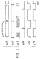
- Fig. 4 is a timing diagram showing the waveforms of various signals in the drive apparatus of Fig. 3.
- Fig. 5 is a block diagram of an essential part of a drive apparatus for an optical element array according to a second embodiment of this invention.
- Fig. 6 is a block diagram of the clock signal selector of Fig. 5.
- Figs. 7 and 8 are block diagrams of the comparators of Fig. 5 respectively.
- Figs. 9(A) and 9(B) are timing diagrams showing the waveforms of various signals in the drive apparatus of Fig. 5.
- a prior art apparatus functions to drive a linear array 11 of LEDs.
- the linear array 11 of the LEDs corresponds to one horizontal line, and the LEDs correspond to pixels respectively.
- the prior art apparatus of Fig. 1 includes a driver 12, a corrective ROM (read-only memory) 13, an address counter 14, a conversion ROM 15, a serial-to-parallel (P/S) converter 16, a latch 17, and a chopper generator 18.
- a digital image signal PIX is inputted sequentially peel by pixel, with plural bits representative of each pixel being in parallel.
- the image signal PIX has "n" bits per pixel.
- a clock signal CK is synchronized with each bit of the image signal PIX.
- a line clock signal LCK is synchronized with each shift of the image signal PIX which corresponds to one horizontal line.
- the driver 12 serves to drive the LEDs of the array 11.
- the corrective ROM 13 stores data for correcting variations between quantities of emitted light from the respective LEDs.
- the corrective data have N bits per LED.
- the address counter 14 generates an address in response to the clock signal CK and the line clock signal LCK, the address being fed to the corrective ROM 13 and being used in reading out the corrective data from the corrective ROM 13.
- the corrective data corresponding to each pixel of the image signal PIX are read out from the corrective ROM 13 in response to the address.
- the corrective data have N bits per pixel.
- the conversion ROM 15 receives the N-bit corrective signal from the corrective ROM 13.
- the conversion ROM 15 also receives the n-bit image signal PIX.
- the conversion ROM 15 generates a Q-bit corrected image signal *PIX which agrees with a multiplication or product of the N-bit corrective signal and the n-bit image signal PIX.
- the P/S converter 16 receives the Q-bit corrected signal *PIX from the conversion ROM 15, and stores a 1-line quantity of the Q-bit corrected signal *PIX. Each time storing a 1-line quantity of the Q-bit corrected signal *PIX into the P/S converter 16 is completed, the P/S converter 16 outputs the 1-line quantity of the corrected signal in parallel.
- the latch 17 receives the 1-line corrected signal from the P/S converter 16, and takes in the 1-line corrected signal at a timing determined by a strobe signal STB generally having a horizontal scanning period. The latch 17 continues to hold the 1-line corrected signal until processing or recording of the corresponding line is completed.
- the chopper generator 18 receives the 1-line corrected signal from the latch 17.
- the chopper generator 18 includes sections corresponding to the LEDs in the array 11 respectively and generating chopper signals in response to the 1-line corrected signal.
- the generated chopper signals correspond to the LEDs in the array 11 respectively.
- the chopper signals are sequentially outputted from the chopper generator 18 to the driver 12 in synchronism with the clock signal CK.
- the chopper signals are binary, having duty cycles depending on the corrected data from the latch 17.
- the driver 12 drives the LEDs in response to the chopper signals respectively in a time-division manner. Specifically, the driver 12 feeds drive currents to the LEDs during the high-level periods of the chopper signals respectively.
- the intervals of light emission from the LEDs are controlled in accordance with the corrective data so as to compensate for differences between the light-emission characteristics of the LEDs. Furthermore, the intervals of light emission from the LEDs are controlled in response to the input image signal PIX.
- the chopper generator 18 has sections corresponding to the LEDs in the array 11 respectively.
- the latch 17 has sections corresponding to the LEDs in the array 11 respectively.
- a section 22 of the latch 17 is followed by a section 21 of the chopper generator 18.
- the section 21 of the chopper generator 18 is connected in series with a section 23 of the driver 23 and an LED 24 in the array 11.
- the section 21 of the chopper generator includes a comparator 25, a counter 26, and a JK flip-flop 27.
- the counter 26 counts pulses of the clock signal CK, and is periodically reset at a predetermined period.
- the comparator 25 compares the output image data from the section 22 of the latch and the output signal from the counter 26, and outputs an identity signal when the image data and the counter signal are equal to each other.
- the JK flip-flop 27 outputs a pulse which starts at a fixed timing and which ends in response to the identity signal outputted from the comparator 25. Thus, the width of the output pulse from the JK flip-flop 27 depends on the image data.
- the section 23 of the driver drives the LED 24 in response to the output pulse from the JK flip-flop 27.
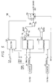
- a drive apparatus for an optical element array includes processing units 1, a shift register 2 connected to the processing units 1, a counter 4 connected to the processing units 1, and a delay circuit 10 connected to the processing units 1.
- the processing units 1 have similar structures, and are connected to LEDs 9 in a linear array 3 respectively.
- the processing units 1 correspond to the LEDs 9 respectively.
- the linear array 3 of the LEDs 9 corresponds to one horizontal line, and the LEDs 9 correspond to pixels respectively.
- Each processing unit 1 includes a latch 5, a comparator 6, a flip-flop 7, and a driver 8.
- the image signal DATA has "n" bits per pixel, which are inputted in parallel.
- the image signal DATA agrees with the result of correcting an original image signal to compensate for variations among the characteristics of the LEDs 9 in the array 3.
- the corrected image signal DATA is generated as in the prior art apparatus of Figs. 1 and 2.
- a reference clock signal CLK is synchronized with each bit of the image signal DATA.
- a reference line clock signal LCLK has a period corresponding to a period of 1-line drive, and is thus synchronized with each 1-line drive.
- the image signal DATA is fed to the shift register 2, and is stored into the shift register 2.
- the shift register 2 includes a series combination of storage sections corresponding to pixels respectively.
- the shift register 2 has a capacity corresponding to the product of the number of pixels and the bit number "n" of the image signal DATA, that is, a capacity for storing a 1-line quantity of the image signal DATA.
- Pixel-corresponding time segments of the image signal DATA are sequentially inputted into the shift register 2, being sequentially shifted from storage sections to subsequent storage sections in the shift register 2.
- the storage sections of the shift register 2 are connected to the latches 5 of the processing units 1 respectively.
- the latches 5 of the processing units 1 take in the pixel-corresponding output image data from the storage sections of the shift register 2 respectively in response to the line clock signal LCLK.
- the pixel-corresponding image data are fed from the latch 5 to the comparator 6.
- the latch 5 and the comparator 6 have capacities corresponding to n-bit signal quantities.
- the counter 4 counts pulses of the clock signal CLK, and outputs a signal representing the number of the counted pulses.
- the counter 4 is periodically reset at a period corresponding to a horizontal scanning period (a 1-line period).
- the output signal from the counter 4 is fed to the comparators 6 of the processing units 1.
- the comparator 6 compares the output signal from the latch 5 and the output signal from the counter 4, and outputs an identity pulse to the flip-flop 7 when the output signal from the latch 5 and the output signal from the counter 4 become equal.
- the moment of the occurrence of an identity pulse depends on the image data fed from the latch 5.
- the delay circuit 10 delays the line clock signal LCLK by a predetermined short time.
- the output signal from the delay circuit 10 is fed to the flip-flops 7 of the processing units 1.
- the flip-flop 7 is set by a pulse of the output signal from the delay circuit 10 and is reset by an identity pulse from the comparator 7 so that the flip-flop 7 outputs a pulse having a duration which equals to the interval between the moment of the occurrence of the pulse of the output signal from the delay circuit 10 and the moment of the occurrence of the identity pulse from the comparator 7.
- the duration of the output pulse from the flip-flop 7 depends on the image data.
- the driver 8 receives the output pulse from the flip-flop 7, and generates a drive pulse current on the basis of the output pulse from the flip-flop 7.
- the drive pulse current is fed from the driver 8 to the corresponding LED 9 so as to activate the LED 9.
- the LED 9 is driven by a drive pulse current having a duration which depends on the duration of an output pulse from the flip-flop 7, that is, which depends on the image data.
- the line clock signal LCLK or the signal (b) has a train of negative pulses.
- the leading edge, that is, the falling edge, of a pulse of the line clock signal LCLK occurs when a 1-line drive period of the image signal DATA or the signal (a) ends.
- the trailing edge, that is, the rising edge, of a pulse of the line clock signal LCLK occurs immediately before a next 1-line drive period of the image signal DATA or the signal (a) starts.
- the line clock signal LCLK is delayed by the delay circuit 10 by the predetermined short time.
- the output signal from the delay circuit 10 is fed to the flip-flop 7.
- the clock signal CLK has a train of pulses.
- the counter 4 counts pulses of the clock signal CLK, and outputs a signal representing the number of the counted pulses.
- the counter 4 is periodically reset at a predetermined period corresponding to a 1-line period.
- the output signal from the counter 4 is fed to the comparator 6.
- the comparator 6 compares the output signal from the latch 5 and the output signal from the counter 4, and outputs an identity pulse (d) to the flip-flop 7 when the output signal from the latch 5 and the output signal from the counter 4 become equal.
- the flip-flop 7 is set by a pulse of the output signal from the delay circuit 10 and is reset by an identity pulse from the comparator 6.
- the flip-flop 7 outputs a pulse having a duration which equals to the interval between the moment of the occurrence of the pulse of the output signal from the delay circuit 10 and the moment of the occurrence of the output identity pulse from the comparator 7.
- the driver 8 receives the output pulse from the flip-flop 7, and generates a drive pulse current (f) on the basis of the output pulse from the flip-flop 7.
- the output pulse from the flip-flop 7 and the drive pulse current from the driver 8 have equal timing characteristics.
- the drive pulse current is fed from the driver 8 to the corresponding LED 9 so as to activate the LED 9. In this way, the LED 9 is driven by a drive pulse current having a duration which depends on the duration of an output pulse from the flip-flop 7.
- Fig. 5 shows an essential part of a second embodiment of this invention which is similar to the embodiment of Figs. 3 and 4 except for the following design changes.
- the second embodiment includes a pulse width modulator 100 which replaces the combination of a comparator 6 and a flip-flop 7 in each processing unit 1.
- a first counter 30 and a second counter 32 are provided other than each processing unit 1 and used in common for the respective processing units 1.
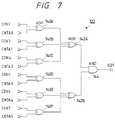
- the pulse width modulator 100 includes a selector 120, comparators 122 and 124, a flip-flop 126, NAND gates 130, 134, and 136, and a NOT gate 132.
- the selector 120 receives four-phase clock signals CLKA, CLKB, CLKC, and CLKD which have a predetermined timing relation with each other as shown in Fig. 9(A). Specifically, the clock signals CLKA-CLKD are out of phase with each other by values corresponding to a half of a 1-pulse width.
- the clock signals CLKA-CLKD are fed from a known clock signal generator (not shown).
- Image data fed from a latch 5 (see Fig. 3) have eight bits DIN0-DIN8.
- the selector 120 receives the two lower bits DIN0 and DIN1 of the image data.
- the selector 120 selects one of the clock signals CLKA-CLKD in response to the two lower bits DIN0 and DIN1 of the image data, and transmits the selected clock signal Z to a T terminal of the flip-flop 126.
- the selector 120 includes NAND gates 121A, 121B, 121C, 121D, and 123, and NOT gates 120A and 120B.
- the clock signals CLKA, CLKB, CLKC, and CLKD are fed to first input terminals of the NAND gates 121A, 121B, 121C, and 121D respectively.
- the first lower bit DIN0 of the image data is fed to second input terminals of the NAND gates 121B and 121D.
- the first lower bit DIN0 of the image data is fed to the input terminal of the NOT gate 120A.
- the output signal from the NOT gate 120A is fed to second input terminals of the NAND gates 121A and 121C.
- the second lower bit DIN1 of the image data is fed to third input terminals of the NAND gates 121C and 121D.
- the second lower bit DIN1 of the image data is fed to the input terminal of the NOT gate 120B.
- the output signal from the NOT gate 120B is fed to third input terminals of the NAND gates 121A and 121B.
- the output signals from the NAND gates 121A-121D are fed to input terminals of the NAND gate 123 respectively.
- the NAND gate 123 outputs a signal Z which agrees with selected one of the clock signals CLKA-CLKD.
- a first counter signal fed from the first counter 30 has six bits CNTA0-CNTA5.
- the bits CNTA0-CNTA5 of the first counter signal are generated from the clock signal CLKA by a plurality of frequency-halving processes.
- the bits CNTA0-CNTA5 of the first counter signal are fed to the comparator 122.
- the comparator 122 compares the six higher bits DIN2-DIN7 of the image data and the bits CNTA0-CNTA5 of the first counter signal.
- the comparator 122 outputs a high-level signal EQ1 when the six higher bits DIN2-DIN7 of the image data coincide with the bits CNTA0-CNTA5 of the first counter signal. Otherwise, the comparator 122 outputs a low-level signal EQ1.
- a second counter signal fed from the second counter 32 has six bits CNTB0-CNTB5. As understood from Fig. 9(B), the bits CNTB0-CNTB5 of the second counter signal are generated from the clock signal CLKC by a plurality of frequency-halving processes. The bits CNTB0-CNTB5 of the second counter signal are fed to the comparator 124. The comparator 124 compares the six higher bits DIN2-DIN7 of the image data and the bits CNTB0-CNTB5 of the second counter signal.
- the comparator 124 outputs a high-level signal EQ2 when the six higher bits DIN2-DIN7 of the image data coincide with the bits CNTB0-CNTB5 of the second counter signal. Otherwise, the comparator 124 outputs a low-level signal EQ2.
- the comparator 122 includes Exclusive-OR gates 140A-140F, NOR gates 142A and 142B, and an AND gate 144.
- the six higher bits DIN2-DIN7 of the image data are fed to first input terminals of the Exclusive-OR gates 140A-140F respectively.
- the bits CNTA0-CNTA5 of the first counter signal are fed to second input terminals of the Exclusive-OR gates 140A-140F respectively.
- the output signals from the Exclusive-OR gates 140A-140C are fed to input terminals of the NOR gate 142A respectively.
- the output signals from the Exclusive-OR gates 140D-140F are fed to input terminals of the NOR gate 142B respectively.
- the output signals from the NOR gates 142A and 142B are fed to input terminals of the AND gate 144 respectively.
- the AND gate 144 outputs a signal EQ1 representing whether or not the six higher bits DIN2-DIN7 of the image data coincide with the bits CNTA0-CNTA5 of the first counter signal.
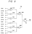
- the comparator 124 includes Exclusive-OR gates 146A-146F, NOR gates 148A and 148B, and an AND gate 150.
- the six higher bits DIN2-DIN7 of the image data are fed to first input terminals of the Exclusive-OR gates 146A-146F respectively.
- the bits CNTB0-CNTB5 of the second counter signal are fed to second input terminals of the Exclusive-OR gates 146A-146F respectively.
- the output signals from the Exclusive-OR gates 146A-146C are fed to input terminals of the NOR gate 148A respectively.
- the output signals from the Exclusive-OR gates 146D-146F are fed to input terminals of the NOR gate 148B respectively.
- the output signals from the NOR gates 148A and 148B are fed to input terminals of the AND gate 150 respectively.
- the AND gate 150 outputs a signal EQ2 representing whether or not the six higher bits DIN2-DIN7 of the image data coincide with the bits CNTB0-CNTB5 of the second counter signal.
- the output signal EQ1 from the comparator 122 is fed to a first input terminal of the NAND gate 130.
- the second lower bit DIN1 of the image data is fed to the input terminal of the NOT gate 132, and is inverted by the NOT gate 132.
- the output signal from the NOT gate 132 is fed to a second input terminal of the NAND gate 130.
- the second lower bit DIN1 of the image data is also fed to a first input terminal of the NAND gate 134.
- the output signal EQ2 from the comparator 124 is fed to a second input terminal of the NAND gate 134.
- the output signals from the NAND gates 130 and 134 are fed to input terminals of the NAND gate 136.
- the NAND gate 136 outputs a signal EQ to a J terminal and a K terminal of the flip-flop 126.
- a pulse signal CLR is fed to a clear terminal DR of the flip-flop 126.
- the pulse signal CLR has a fixed timing relation with the start of the clock signal CLKA and the counter signal bit CNTA0. Thus, the pulse signal CLR is synchronous with a horizontal scanning process.
- the pulse signal CLR is fed from a known pulse generator (not shown).
- the QB output signal from the flip-flop 126 is fed to a driver 8 (see Fig. 3).
- the pulse width modulator 100 of Fig. 5 operates as follows.
- the selector 120 selects one of the clock signals CLKA-CLKD in response to the two lower bits DIN0 and DIN1 of the image data, and transmits the selected clock signal Z to the T terminal of the flip-flop 126.
- the comparator 122 compares the six higher bits DIN2-DIN7 of the image data and the bits CNTA0-CNTA5 of the first counter signal.
- the comparator 122 outputs a high-level identity signal EQ1 when the six higher bits DIN2-DIN7 of the image data coincide with the bits CNTA0-CNTA5 of the first counter signal. Otherwise, the comparator 122 outputs a low-level signal EQ1.
- the duration or width of a high-level pulse in the output signal EQ1 from the comparator 122 agrees with the pulse width of the counter signal bit CNTA0 which is the narrowest among the pulse widths of the counter signal bits CNTA0-CNTA5.
- the comparator 124 compares the six higher bits DIN2-DIN7 of the image data and the bits CNTB0-CNTB5 of the second counter signal.
- the comparator 124 outputs a high-level identity signal EQ2 when the six higher bits DIN2-DIN7 of the image data coincide with the bits CNTB0-CNTB5 of the second counter signal. Otherwise, the comparator 124 outputs a low-level signal EQ2.
- the duration or width of a high-level pulse in the output signal EQ2 from the comparator 124 agrees with the pulse width of the counter signal bit CNTB0 which is the narrowest among the pulse widths of the counter signal bits CNTB0-CNTB5.
- the NAND gates 30, 34, 36, and the NOT gate 132 compose a selector which selects one of the output signals EQ1 and EQ2 from the comparators 122 and 124 in response to the second lower bit DIN1 of the image data. Specifically, the output signal EQ1 from the comparator 122 is selected when the second lower bit DIN1 of the image data is in a low level state. The output signal EQ2 from the comparator 124 is selected when the second lower bit DIN1 of the image data is in a high level state. Selected one of the output signals EQ1 and EQ2 from the comparators 122 and 124 is fed to the J terminal and the K terminal of the flip-flop 126 as an identity signal EQ.
- the output signal DOT from the pulse width modulator 100 is reversed in response to the clock signal fed to the T terminal of the flip-flop 126. During other periods, the transition of the output signal DOT from the pulse width modulator 100 is inhibited.
- the timing of the transition of the output signal DOT is determined by one of the clock signals CLKA-CLKD which is selected by the selector 120. Therefore, as shown in Fig. 9(A), the pulse width of the output signal DOT can be determined by four timings selected in response to the two lower bits DIN0 and DIN1 of the image data.
- the pulse signal CLR is fed to the clear terminal of the flip-flop 126 so as to control a timing of the start of a pulse of the output signal DOT. Specifically, each pulse of the output signal DOT starts at a constant timing which agrees with the moment of the start of pulses of the clock signal CLKA and the counter signal bit CNTA0.
Landscapes
- Physics & Mathematics (AREA)
- Engineering & Computer Science (AREA)
- Optics & Photonics (AREA)
- General Engineering & Computer Science (AREA)
- General Physics & Mathematics (AREA)
- Theoretical Computer Science (AREA)
- Control Of El Displays (AREA)
- Led Devices (AREA)
Applications Claiming Priority (4)
| Application Number | Priority Date | Filing Date | Title |
|---|---|---|---|
| JP336122/90 | 1990-11-30 | ||
| JP2336122A JPH04206783A (ja) | 1990-11-30 | 1990-11-30 | 光素子アレイ駆動装置 |
| JP155266/91 | 1991-05-31 | ||
| JP3155266A JPH04354418A (ja) | 1991-05-31 | 1991-05-31 | パルス幅変調回路 |
Publications (3)
| Publication Number | Publication Date |
|---|---|
| EP0487971A2 true EP0487971A2 (de) | 1992-06-03 |
| EP0487971A3 EP0487971A3 (en) | 1993-07-14 |
| EP0487971B1 EP0487971B1 (de) | 1996-08-14 |
Family
ID=26483311
Family Applications (1)
| Application Number | Title | Priority Date | Filing Date |
|---|---|---|---|
| EP91119275A Expired - Lifetime EP0487971B1 (de) | 1990-11-30 | 1991-11-12 | Steuergerät für Anordnung von optischen Elementen |
Country Status (3)
| Country | Link |
|---|---|
| US (1) | US5250939A (de) |
| EP (1) | EP0487971B1 (de) |
| DE (1) | DE69121365T2 (de) |
Families Citing this family (8)
| Publication number | Priority date | Publication date | Assignee | Title |
|---|---|---|---|---|
| KR960006814B1 (ko) * | 1993-05-31 | 1996-05-23 | 삼성전자주식회사 | 전자사진 방식 프린터의 광신호 제어방법 및 장치 |
| US5815187A (en) * | 1996-01-11 | 1998-09-29 | Xante Corporation | Method for improving the dimensional accuracy of laser printers |
| JP3620310B2 (ja) * | 1998-10-16 | 2005-02-16 | 富士ゼロックス株式会社 | パルス発生装置および画像記録装置 |
| US6268751B1 (en) * | 1998-12-16 | 2001-07-31 | Texas Instruments Incorporated | Duty cycle optimized prescaler |
| JP2001312246A (ja) * | 2000-05-01 | 2001-11-09 | Sony Corp | 変調回路およびこれを用いた画像表示装置 |
| US7148910B2 (en) * | 2003-11-06 | 2006-12-12 | Eastman Kodak Company | High-speed pulse width modulation system and method for linear array spatial light modulators |
| JP4360410B2 (ja) * | 2007-03-16 | 2009-11-11 | セイコーエプソン株式会社 | 画像処理回路、表示装置及び印刷装置 |
| US11076464B2 (en) * | 2019-09-06 | 2021-07-27 | Novatek Microelectronics Corp. | Control method and driving circuit for light emitting diode |
Family Cites Families (8)
| Publication number | Priority date | Publication date | Assignee | Title |
|---|---|---|---|---|
| JPS58162988A (ja) * | 1982-03-23 | 1983-09-27 | 日本電気株式会社 | 表示装置 |
| US4596995A (en) * | 1983-06-24 | 1986-06-24 | Canon Kabushiki Kaisha | Dot printer having means for correcting intensity variations |
| JPS61111061A (ja) * | 1984-11-05 | 1986-05-29 | Casio Comput Co Ltd | 記録装置 |
| US4855760A (en) * | 1987-03-12 | 1989-08-08 | Fuji Photo Film Co., Ltd. | LED array with graduated quantity control |
| JPS63270167A (ja) * | 1987-04-30 | 1988-11-08 | Fuji Photo Film Co Ltd | 画像形成方法 |
| US4746941A (en) * | 1987-10-13 | 1988-05-24 | Eastman Kodak Company | Dot printer with token bit selection of data latching |
| JPH024547A (ja) * | 1988-06-23 | 1990-01-09 | Matsushita Graphic Commun Syst Inc | 発光素子駆動装置 |
| JPH02160285A (ja) * | 1988-12-14 | 1990-06-20 | Clarion Co Ltd | Lcd制御装置 |
-
1991
- 1991-11-05 US US07/787,867 patent/US5250939A/en not_active Expired - Fee Related
- 1991-11-12 EP EP91119275A patent/EP0487971B1/de not_active Expired - Lifetime
- 1991-11-12 DE DE69121365T patent/DE69121365T2/de not_active Expired - Fee Related
Also Published As
| Publication number | Publication date |
|---|---|
| EP0487971A3 (en) | 1993-07-14 |
| US5250939A (en) | 1993-10-05 |
| DE69121365D1 (de) | 1996-09-19 |
| DE69121365T2 (de) | 1996-12-12 |
| EP0487971B1 (de) | 1996-08-14 |
Similar Documents
| Publication | Publication Date | Title |
|---|---|---|
| US4368491A (en) | Driving equipment for multi-gradation level reproduction | |
| US5371524A (en) | End pulse width modulation for digital image printer with halftone gray scale capability | |
| US4443121A (en) | Thermal printing apparatus with reference gray scale comparator | |
| US4455578A (en) | Electronics for arrayed photosources | |
| US4204233A (en) | Electronic facet error correction for laser scanning | |
| US5457488A (en) | Method and apparatus for controlling array of light-emitting elements | |
| JPS6254676B2 (de) | ||
| JPH057910B2 (de) | ||
| US5250939A (en) | Drive apparatus for optical element array | |
| US4845520A (en) | System for driving a thermal print head for constant dot density | |
| US5428321A (en) | Pulse width modulator having controlled delay circuit | |
| US5245355A (en) | Method and apparatus for grey level printing with amplitude and pulsewidth modulation | |
| US4963989A (en) | Method and apparatus for grey level printing | |
| US5128692A (en) | Symmetric binary weighted exposure method and apparatus employing center pulse width modulation for continuous tone printer | |
| EP0067587B1 (de) | Elektrostatisches Aufzeichnungsgerät | |
| US6061078A (en) | Non-impact printer apparatus and method of printing with improved control of emitter pulsewidth modulation duration | |
| US5657069A (en) | Method and apparatus for grey level printing | |
| EP0476863A1 (de) | Verfahren und Drucker zum Druck eines Bildes, welches aus zweidimensional angeordneten Bildelementen besteht | |
| JPH024547A (ja) | 発光素子駆動装置 | |
| JP2785642B2 (ja) | 階調記録方法 | |
| JP2808995B2 (ja) | 印字ヘッド制御装置 | |
| US4916546A (en) | Image organizing unit of a laser beam printer | |
| KR100245800B1 (ko) | 칼라프린터의 서멀헤드 구동장치 | |
| JP3179962B2 (ja) | Ledアレイの駆動制御回路 | |
| JPH04206783A (ja) | 光素子アレイ駆動装置 |
Legal Events
| Date | Code | Title | Description |
|---|---|---|---|
| PUAI | Public reference made under article 153(3) epc to a published international application that has entered the european phase |
Free format text: ORIGINAL CODE: 0009012 |
|
| AK | Designated contracting states |
Kind code of ref document: A2 Designated state(s): DE FR GB |
|
| PUAL | Search report despatched |
Free format text: ORIGINAL CODE: 0009013 |
|
| AK | Designated contracting states |
Kind code of ref document: A3 Designated state(s): DE FR GB |
|
| 17P | Request for examination filed |
Effective date: 19930824 |
|
| 17Q | First examination report despatched |
Effective date: 19950721 |
|
| GRAH | Despatch of communication of intention to grant a patent |
Free format text: ORIGINAL CODE: EPIDOS IGRA |
|
| GRAH | Despatch of communication of intention to grant a patent |
Free format text: ORIGINAL CODE: EPIDOS IGRA |
|
| GRAA | (expected) grant |
Free format text: ORIGINAL CODE: 0009210 |
|
| AK | Designated contracting states |
Kind code of ref document: B1 Designated state(s): DE FR GB |
|
| ET | Fr: translation filed | ||
| REF | Corresponds to: |
Ref document number: 69121365 Country of ref document: DE Date of ref document: 19960919 |
|
| PLBE | No opposition filed within time limit |
Free format text: ORIGINAL CODE: 0009261 |
|
| STAA | Information on the status of an ep patent application or granted ep patent |
Free format text: STATUS: NO OPPOSITION FILED WITHIN TIME LIMIT |
|
| 26N | No opposition filed | ||
| PGFP | Annual fee paid to national office [announced via postgrant information from national office to epo] |
Ref country code: FR Payment date: 19991109 Year of fee payment: 9 |
|
| PGFP | Annual fee paid to national office [announced via postgrant information from national office to epo] |
Ref country code: GB Payment date: 19991110 Year of fee payment: 9 |
|
| PGFP | Annual fee paid to national office [announced via postgrant information from national office to epo] |
Ref country code: DE Payment date: 19991115 Year of fee payment: 9 |
|
| PG25 | Lapsed in a contracting state [announced via postgrant information from national office to epo] |
Ref country code: GB Free format text: LAPSE BECAUSE OF NON-PAYMENT OF DUE FEES Effective date: 20001112 |
|
| GBPC | Gb: european patent ceased through non-payment of renewal fee |
Effective date: 20001112 |
|
| PG25 | Lapsed in a contracting state [announced via postgrant information from national office to epo] |
Ref country code: FR Free format text: LAPSE BECAUSE OF NON-PAYMENT OF DUE FEES Effective date: 20010731 |
|
| PG25 | Lapsed in a contracting state [announced via postgrant information from national office to epo] |
Ref country code: DE Free format text: LAPSE BECAUSE OF NON-PAYMENT OF DUE FEES Effective date: 20010801 |
|
| REG | Reference to a national code |
Ref country code: FR Ref legal event code: ST |