EP0486991A2 - Programmierbare logische Schaltung - Google Patents
Programmierbare logische Schaltung Download PDFInfo
- Publication number
- EP0486991A2 EP0486991A2 EP91119638A EP91119638A EP0486991A2 EP 0486991 A2 EP0486991 A2 EP 0486991A2 EP 91119638 A EP91119638 A EP 91119638A EP 91119638 A EP91119638 A EP 91119638A EP 0486991 A2 EP0486991 A2 EP 0486991A2
- Authority
- EP
- European Patent Office
- Prior art keywords
- circuit
- user
- logic
- logic circuit
- pld
- Prior art date
- Legal status (The legal status is an assumption and is not a legal conclusion. Google has not performed a legal analysis and makes no representation as to the accuracy of the status listed.)
- Ceased
Links
- 108090000553 Phospholipase D Proteins 0.000 description 48
- 230000010354 integration Effects 0.000 description 16
- 238000010586 diagram Methods 0.000 description 12
- 230000006870 function Effects 0.000 description 4
- 102100032967 Phospholipase D1 Human genes 0.000 description 2
- 108010002266 phospholipase D1 Proteins 0.000 description 2
- 230000004044 response Effects 0.000 description 2
- 238000010276 construction Methods 0.000 description 1
- 238000009877 rendering Methods 0.000 description 1
- 230000003068 static effect Effects 0.000 description 1
Images




Classifications
-
- H—ELECTRICITY
- H03—ELECTRONIC CIRCUITRY
- H03K—PULSE TECHNIQUE
- H03K19/00—Logic circuits, i.e. having at least two inputs acting on one output; Inverting circuits
- H03K19/02—Logic circuits, i.e. having at least two inputs acting on one output; Inverting circuits using specified components
- H03K19/173—Logic circuits, i.e. having at least two inputs acting on one output; Inverting circuits using specified components using elementary logic circuits as components
- H03K19/177—Logic circuits, i.e. having at least two inputs acting on one output; Inverting circuits using specified components using elementary logic circuits as components arranged in matrix form
- H03K19/17748—Structural details of configuration resources
- H03K19/1776—Structural details of configuration resources for memories
-
- H—ELECTRICITY
- H03—ELECTRONIC CIRCUITRY
- H03K—PULSE TECHNIQUE
- H03K19/00—Logic circuits, i.e. having at least two inputs acting on one output; Inverting circuits
- H03K19/02—Logic circuits, i.e. having at least two inputs acting on one output; Inverting circuits using specified components
- H03K19/173—Logic circuits, i.e. having at least two inputs acting on one output; Inverting circuits using specified components using elementary logic circuits as components
- H03K19/177—Logic circuits, i.e. having at least two inputs acting on one output; Inverting circuits using specified components using elementary logic circuits as components arranged in matrix form
- H03K19/17704—Logic circuits, i.e. having at least two inputs acting on one output; Inverting circuits using specified components using elementary logic circuits as components arranged in matrix form the logic functions being realised by the interconnection of rows and columns
-
- H—ELECTRICITY
- H03—ELECTRONIC CIRCUITRY
- H03K—PULSE TECHNIQUE
- H03K19/00—Logic circuits, i.e. having at least two inputs acting on one output; Inverting circuits
- H03K19/02—Logic circuits, i.e. having at least two inputs acting on one output; Inverting circuits using specified components
- H03K19/173—Logic circuits, i.e. having at least two inputs acting on one output; Inverting circuits using specified components using elementary logic circuits as components
- H03K19/177—Logic circuits, i.e. having at least two inputs acting on one output; Inverting circuits using specified components using elementary logic circuits as components arranged in matrix form
- H03K19/17724—Structural details of logic blocks
- H03K19/17728—Reconfigurable logic blocks, e.g. lookup tables
Definitions
- This invention relates to a programmable logic device having a memory circuit for storing circuit configuration data and a logic gate block for realizing a logic circuit desired by a user on the basis of circuit configuration data written into the memory circuit, and more particularly to a programmable logic device improved in the degree of integration.
- PLD programmable logic device
- N-channel MOS transistors and P-channel MOS transistors are used as switching elements (transfer gates).
- configuration of on-state or off-state of the switching elements for configurating a circuit of a logic circuit desired by the user in the logic gate block is determined in accordance with data of a memory circuit for storing circuit configuration data. Accordingly, the user can perform configuration of the logic circuit desired by the user by writing the circuit configuration data into this memory circuit for storing the circuit configuration data.
- the present invention has been developed to obviate the above-described conventional problems and has as its object the provision of a PLD capable of effectively improving the degree of integration of a logic circuit desired by a user in the PLD.
- a switching circuit for controlling at least a part of a circuit for writing the circuit configuration data into the memory circuit so as to be utilized as a cart of the logic circuit desired by the user after the circuit configuration.
- At least the part of the circuit to be utilized is made to be a wiring used when the data are written into the memory circuit.
- At least part of the circuit to be utilized is made to be a driver or a column selector used when the data are written into the memory circuit.
- At least a part of the circuit configuration circuit which has heretofore been used only for programming the logic circuit of the user, is made to be usable as a part of the programmed logic circuit desired by the user after this logic circuit of the user is programmed.
- the inventor has found such an arrangement that the switching circuit is provided for controlling at least the part of the circuit configuration circuit used when the logic circuit desired by the user is programmed to be utilizable as the part of the logic circuit desired by the user after the circuit configuration.
- Fig. 1 is a block diagram showing the gist of the present invention.
- a circuit configuration circuit 10 is a circuit used when the logic circuit desired by the user is programmed, and includes not only the driver or the column selector but also wirings for this purpose.
- a user logic circuit 12 is a logic circuit desired by the user, which is programmed and configurated in a gate block, mainly in the PLD.
- the logic circuit desired by the user is not constituted only by logic bates in this logic gate block, but, also constituted by other logic gates and wirings in the PLD, such for example as an input buffer gate, an output buffer gate and various wirings.
- this user logic circuit 12 includes all of the logic gates and wirings, which constitute the logic circuit of the user in the PLD.
- wirings such as bit lines and word lines are laid between respective memory elements of the memory circuit for storing the circuit configuration data for programming the logic circuit of the user.
- the wirings such as these bit lines and word lines are formed of relatively long continuous wirings.
- some part of wirings of the logic circuit desired by the user and configurated by the user may include ones analogous to the above-described wirings between the memory elements. Accordingly, the above-described analogous wirings are commonly used, so that the degree of integration of the PLD can be improved.
- writing of the circuit configuration data into the memory circuit for storing the circuit configuration data of the PLD is performed at every memory cell of the integrated circuit of the PLD, and, when memory cell selection of the corresponding PLD for write-in of the circuit configuration data is performed by a plurality of address lines, a gate circuit as being an address decoder becomes necessary in this circuit configuration circuit 10.
- the logic circuits may be formed per PLD, and, when memory cell selection of the corresponding PLD for selecting the logic circuit configurated by user per PLD as described above is performed by a plurality of address lines, an address decoder becomes necessary in the user logic circuit 12.
- the both address decoders are completely identical or substantially identical with each other. Accordingly, when the address decoder in the circuit configuration circuit 10 and the address decoder in the user logic circuit 12 are commonly used, the degree of integration of the PLD as a whole can be improved.
- the inventor has formed the wirings and the analogous circuits of the gate circuits into a common circuit 14 which can be commonly used for the circuit configuration circuit 10 and the user logic circuit 12.
- the analogous circuits between the circuit configuration circuit and the user logic circuit are formed into a common circuit, so that the degree of integration of the logic circuit desired by the user in the PLD can be improved.
- Fig. 2 is the block diagram showing the first embodiment of the present invention.
- the common circuit between the circuit configuration circuit used when the logic circuit desired by the user is configurated and the user logic circuit realized by this configurating is formed to provide a common line 14a.
- the circuit configuration circuit is indicated by a circuit for writing configuration data (driver, column selector) 10a and a circuit for storing configuration data (memory cell such as SRAM (static random access memory) cell, EPROM (electrically programmable read only memory) cell and so on) 10b.
- configuration data memory cell such as SRAM (static random access memory) cell, EPROM (electrically programmable read only memory) cell and so on
- user logic circuit is indicated by 12a and 12b.
- circuit configuration selection signals S1a and S1b to select and switch the common line 14a for either the circuit configuration circuit or the user logic circuit is performed by circuit configuration selection signals S1a and S1b, user logic circuit selection signals S2a and S2b, and the switching elements operated in response to these circuit configuration selection signal S1b and user logic circuit selection signal S2b.
- the circuit configuration selection signal S1a is inputted into the circuits 10a and 10b, and, when this signal is set at "1", the circuits 10a and 10b are brought into enable states.
- the circuit configuration selection signal S1b ON-OFF operates a switching element as being an object of control, and, when this signal is set at "1", the corresponding switching element is brought into an ON state.
- the user logic circuit selection signal S2a is inputted into the user logic circuits 12a and 12b, and, when this signal is set at "1", these user logic circuits 12a and 12b are brought into enable states.
- the user logic circuit selection signal S2b ON-OFF operates a switching element as being an object of control, and, when this signal is set at "1", the corresponding switching element is brought into an ON state.
- the circuit configuration selection signals S1a and S1b are set at "1"
- the user logic circuit selection signals S2a and S2b are set at "0".
- the circuit 10a and 10b are brought into the enable states, while the user logic circuits 12a and 12b are brought into unable states.
- connected to the common line 14a are only the circuits 10a and 10b.
- the logic circuit desired by the user is configurated in the PLD, and, when this configurated logic circuit is used, the circuit configuration selection signals S1a and S1b are set at "0", while the user logic selection signals S2a and S2b are set at "1". Accordingly, at this time, the circuits 10a and 10b are brought into unable states, while the user logic circuits 12a and 12b are brought into the enable states. Simultaneously, connected to the common line 14a are only the user logic circuits 12a and 12b.
- one and the same common line 14a can be switched for common use between the circuits 10a and 10b as being the circuit configuration circuits and the user logic circuits 12a and 12b, with the both pairs of circuits being not operated, and not concurring at the same time, so that the amount of wirings in the PLD can be reduced and the degree of integration in the PLD can be improved.
- circuit configuration selection signal S1a or the user logic circuit selection signal S2a is set at "0"
- the respective circuits 10a, 10b, 12a and 12b are brought into the unable states, whereby, when the states of being connected to the common line 14a is released, it is needless to say that there is no need of making the connection to the common line 14a to be undone anew by setting the circuit configuration selection signal S1b or the user logic circuit selection signal S2b at "0". That is, the switching element for this switching operation may be provided as necessary.
- circuits 10a, 10b, 12a and 12b are released from the connection to the common line 14a by the switching operation in response to the circuit configuration selection signal S1b or the user logic circuit selection signal S2b, whereby, when there is no need of the circuits being brought into a non-active state anew, it is needless to say that there is no need of providing the circuits with a function of inputting the circuit configuration selection signal S1a and the user logic circuit selection signal S2a to switch for either the active state or the non-active state.
- bit lines, word lines and the like may be used, for example.
- bit lines, word lines and the like include ones having relatively long wiring lengths, and, when these wirings are commonly used between the circuit configuration circuit and the user logic circuit, the degree of integration of the logic circuit desired by the user in the PLD can be improved.
- Fig. 3 is the block diagram showing the second embodiment of the present invention.
- a common driver (date circuit) 14b serving as the common circuit between the circuit configuration circuit and the user logic circuit.
- the circuit configuration circuits used for configurating the logic circuit desired by the user are memory cells 10c and 10d. Furthermore, the user logic circuits as being the logic circuits desired by the user, which are programmed and realized, are 12c and 12d.
- reference characters S1a, S1b, S2a and S2b designate those identical with ones having the same reference characters in Fig. 2.
- the circuit configuration selection signals S1a and S1b are set at "1"
- the user logic circuit selection signals S2a and S2b are set at "0”
- the common driver 14b is connected to the user logic circuit 10c to function as a part of the circuit configuration circuit.
- the circuit configuration selection signals S1a and S1b are set at "0"
- the user logic circuit selection signals S2a and S2b are set at "1”
- the common driven 14b is connected to the user logic circuit 12c to function as a part of the user logic circuit.
- circuit configuration selection signals S1a and S1b should not necessarily be used as shown in Fig. 3
- all of the user logic circuit selection signals S2a and S2b should not necessarily be used as shown in Fig. 3, and these signals should be examined for necessity of provision.
- an address decoder to be described hereunder in the fourth embodiment of the present invention and an output buffer gate for driving an output to the outside of the PLD may be included.
- Some of the outputs to the outside of the PLD may have high load to be driven, and, the transistor size for driving the output buffer gate in this case is made to be large. Accordingly, when the second embodiment of the present invention is applied thereto, for example, the output buffer gate having the large transistor size and the large integrated circuit layout size is commonly used between the circuit configuration circuit and the user logic circuit, the degree of integration of the logic circuit desired by the user in the PLD can be improved.
- Fig. 4 is the block diagram showing the third embodiment of the present invention.
- the common circuit commonly used between the circuit configuration circuit used when the logic circuit desired by the user is configurated and the user logic circuit realized by this configuration, which is used after this configuration, is a bit line 14c.
- switching circuits commonly used for this common circuits are totally two switching circuits 20a and totally two switching circuits 20b.
- bit line 14c when the logic circuit desired by the user is configurated, the bit line 14c is connected to a bit line driver 10e to function as an intrinsic bit line, and writing of the circuit configuration data into totally eight circuit configuration data memory (memory cell) M by this bit line driver 10e is performed.
- This circuit configuration data memory M performs the configuration of connection of allotted switching station elements SS and the configuration of logic circuits of allotted logic gate blocks 30, in accordance with the written- in circuit configuration data.
- circuit configuration data memory M to the switching station elements SS and the logic gate blocks 30 are shown by broken lines in this Fig. 4.
- the bit line 14c is connected to the switching station elements SS through a switching circuit 20a or 20b, or connected to the logic gate blocks 30 through the switching station elements SS, so as to be used as a part of the configurated logic circuit desired by the user.
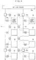
- Fig. 5 is the circuit diagram of the aforesaid switching circuit used in the third embodiment.
- reference characters 10e, 14c, 20a, 20b and SS designate those identical with ones having the same reference characters in Fig. 4.
- the switching circuit 20a for switching from a wiring from the bit line driver 10e to a wiring from the switching station element SS or vice versa to connect either one of the above-mentioned wirings to the bit line 14c is constituted by totally two N-channel MOS transistors TN1, TN2 and an inverter gate 40.
- a switching signal S is set at "1", when the logic circuit desired by the user is configurated, and, set at "0" when the configurated logic circuit is used.
- the switching signal S is inputted into a gate of the N-channel MOS transistor TN1, and also inputted into a gate of the N-channel MOS transistor TN2 through the inverter gate 40.
- the N-channel MOS transistor TN1 is brought into the ON state, and the wiring from the bit line driver 10e is connected to the bit line 14c.
- the N-channel MOS transistor TN2 is brought into the ON state, and the wiring from the switching station element SS is connected to the bit line 14c.
- the switching circuit 20b is constituted by an N-channel MOS transistor TN3 and the inverter gate 40.
- This inverter gate 40 is the one, being inputted thereinto with a switching signal S, inverts the logic polarity and outputs this inverted signal into a gate of the N-channel MOS transistor TN3.
- the switching signal S is set at "0"
- the N-channel MOS transistor TN3 is brought into the ON state, and the wiring from the switching station element SS and the bit line 14c are connected to each other.
- the bit lines including ones having relatively long wiring lengths in the PLD can be commonly used with the circuit configuration circuit and the user logic circuit as well, so that the degree of integration of the logic circuit desired by the user in the PLD can be improved.
- Fig. 6 is the block diagram showing the fourth embodiment of the present invention.
- the PLD 1 is constituted by an SRAM cell 10f as being circuit configuration circuit used when the logic circuit desired by the user is configurated, a user logic circuit 12e used after this configuration when the logic circuit realized by the configuration is used, and an address decoder 14d.
- memory cell selection is performed through a plurality of address lines when the logic circuit desired by the user is configurated.
- the address decoder for decoding the address data from the plurality of address lines to determine whether a memory cell is selected or not can be commonly used when the logic circuit desired by the user is configurated and when the logic circuit realized by the configuration is used after this configuration.
- an output from this address decoder 14d is outputted into the memory cell 10f and outputted into the user logic circuit 12 as well.
- the switching signal S is set at "1"
- the memory cell 10f is brought into the active state, and inputted thereinto with an output from the address decoder 14d for functioning.
- the switching signal S is set at "0"
- the user logic circuit 12e having inputted thereinto with the switching signal S, which is inverted, is brought into the active state, and inputted thereinto with an output from the address decoder 14d for functioning.
- the logic gate of the address decoder has a large layout area for the integrated circuit.
- the address decoder can be commonly used between the circuit configuration circuit and the user logic circuit, so that the degree of integration of the logic circuit desired by the user in the PLD can be improved.
Landscapes
- Physics & Mathematics (AREA)
- Mathematical Physics (AREA)
- Engineering & Computer Science (AREA)
- Computer Hardware Design (AREA)
- Computing Systems (AREA)
- General Engineering & Computer Science (AREA)
- Logic Circuits (AREA)
- Design And Manufacture Of Integrated Circuits (AREA)
Applications Claiming Priority (2)
| Application Number | Priority Date | Filing Date | Title |
|---|---|---|---|
| JP313366/90 | 1990-11-19 | ||
| JP2313366A JP2544020B2 (ja) | 1990-11-19 | 1990-11-19 | プログラマブル論理素子 |
Publications (2)
| Publication Number | Publication Date |
|---|---|
| EP0486991A2 true EP0486991A2 (de) | 1992-05-27 |
| EP0486991A3 EP0486991A3 (en) | 1992-10-28 |
Family
ID=18040395
Family Applications (1)
| Application Number | Title | Priority Date | Filing Date |
|---|---|---|---|
| EP19910119638 Ceased EP0486991A3 (en) | 1990-11-19 | 1991-11-18 | Programmable logic device |
Country Status (3)
| Country | Link |
|---|---|
| US (1) | US5282163A (de) |
| EP (1) | EP0486991A3 (de) |
| JP (1) | JP2544020B2 (de) |
Cited By (4)
| Publication number | Priority date | Publication date | Assignee | Title |
|---|---|---|---|---|
| GB2300505A (en) * | 1995-05-02 | 1996-11-06 | Xilinx Inc | Programmable logic with parallel and serial user interfaces |
| GB2300504A (en) * | 1995-05-02 | 1996-11-06 | Xilinx Inc | Programmable switch for logic array input/output signals |
| EP0678985A3 (de) * | 1994-04-20 | 1997-07-23 | Xilinx Inc | Programmierbare logische Vorrichtung, die mehr als eine Konfiguration speichert, und Mittel zum Umschalten der Konfigurationen. |
| US6732263B1 (en) * | 2000-06-12 | 2004-05-04 | Altera Corporation | Configuring both a programmable logic device and its embedded logic with a single serialized configuration bit stream |
Families Citing this family (12)
| Publication number | Priority date | Publication date | Assignee | Title |
|---|---|---|---|---|
| GB9303084D0 (en) * | 1993-02-16 | 1993-03-31 | Inmos Ltd | Programmable logic circuit |
| US5352940A (en) * | 1993-05-27 | 1994-10-04 | Altera Corporation | Ram convertible look-up table based macrocell for PLDs |
| US5768562A (en) * | 1995-09-26 | 1998-06-16 | Altera Corporation | Methods for implementing logic in auxiliary components associated with programmable logic array devices |
| US6147890A (en) * | 1997-12-30 | 2000-11-14 | Kawasaki Steel Corporation | FPGA with embedded content-addressable memory |
| US6144573A (en) * | 1998-06-26 | 2000-11-07 | Altera Corporation | Programmable logic devices with improved content addressable memory capabilities |
| US6453382B1 (en) | 1998-11-05 | 2002-09-17 | Altera Corporation | Content addressable memory encoded outputs |
| JP3269526B2 (ja) | 1999-02-09 | 2002-03-25 | 日本電気株式会社 | プログラマブルロジックlsi |
| US7111110B1 (en) | 2002-12-10 | 2006-09-19 | Altera Corporation | Versatile RAM for programmable logic device |
| JP4643977B2 (ja) * | 2004-11-30 | 2011-03-02 | 富士通株式会社 | プログラマブル・ロジック・デバイス、情報処理装置、プログラマブル・ロジック・デバイスの制御方法 |
| TWI611419B (zh) * | 2012-12-24 | 2018-01-11 | 半導體能源研究所股份有限公司 | 可程式邏輯裝置及半導體裝置 |
| US9294096B2 (en) * | 2014-02-28 | 2016-03-22 | Semiconductor Energy Laboratory Co., Ltd. | Semiconductor device |
| WO2020203220A1 (ja) * | 2019-03-29 | 2020-10-08 | 日本電気株式会社 | 論理集積回路及び論理集積回路による制御方法 |
Family Cites Families (7)
| Publication number | Priority date | Publication date | Assignee | Title |
|---|---|---|---|---|
| AU5450386A (en) * | 1986-02-07 | 1987-08-25 | Silicon Communications Corp. | Electrically erasable programmable logic array (eepla) |
| US4831573A (en) * | 1987-03-06 | 1989-05-16 | Altera Corporation | Programmable integrated circuit micro-sequencer device |
| US4783606A (en) * | 1987-04-14 | 1988-11-08 | Erich Goetting | Programming circuit for programmable logic array I/O cell |
| EP0317287B1 (de) * | 1987-11-20 | 1992-11-11 | Kawasaki Steel Corporation | Programmierbare logische Vorrichtung |
| US4835414A (en) * | 1988-03-14 | 1989-05-30 | Advanced Micro Devices, Inc. | Flexible, reconfigurable terminal pin |
| JPH0263147A (ja) * | 1988-08-29 | 1990-03-02 | Fujitsu Ltd | 冷却装置 |
| US4975601A (en) * | 1989-09-29 | 1990-12-04 | Sgs-Thomson Microelectronics, Inc. | User-writable random access memory logic block for programmable logic devices |
-
1990
- 1990-11-19 JP JP2313366A patent/JP2544020B2/ja not_active Expired - Fee Related
-
1991
- 1991-11-14 US US07/791,405 patent/US5282163A/en not_active Expired - Lifetime
- 1991-11-18 EP EP19910119638 patent/EP0486991A3/en not_active Ceased
Cited By (7)
| Publication number | Priority date | Publication date | Assignee | Title |
|---|---|---|---|---|
| EP0678985A3 (de) * | 1994-04-20 | 1997-07-23 | Xilinx Inc | Programmierbare logische Vorrichtung, die mehr als eine Konfiguration speichert, und Mittel zum Umschalten der Konfigurationen. |
| EP1455455A3 (de) * | 1994-04-20 | 2008-04-09 | Xilinx, Inc. | Programmierbare logische Vorrichtung, die mehr als eine Konfiguration speichert, und Mittel zum Umschalten zwischen den Konfigurationen |
| GB2300505A (en) * | 1995-05-02 | 1996-11-06 | Xilinx Inc | Programmable logic with parallel and serial user interfaces |
| GB2300504A (en) * | 1995-05-02 | 1996-11-06 | Xilinx Inc | Programmable switch for logic array input/output signals |
| GB2300504B (en) * | 1995-05-02 | 1999-08-04 | Xilinx Inc | Programmable switch for fpga input/output signals |
| USRE37195E1 (en) | 1995-05-02 | 2001-05-29 | Xilinx, Inc. | Programmable switch for FPGA input/output signals |
| US6732263B1 (en) * | 2000-06-12 | 2004-05-04 | Altera Corporation | Configuring both a programmable logic device and its embedded logic with a single serialized configuration bit stream |
Also Published As
| Publication number | Publication date |
|---|---|
| US5282163A (en) | 1994-01-25 |
| JPH04188649A (ja) | 1992-07-07 |
| JP2544020B2 (ja) | 1996-10-16 |
| EP0486991A3 (en) | 1992-10-28 |
Similar Documents
| Publication | Publication Date | Title |
|---|---|---|
| EP0486991A2 (de) | Programmierbare logische Schaltung | |
| KR100320605B1 (ko) | 방해없이임의로주소지정가능한메모리시스템 | |
| US5633830A (en) | Random access memory block circuitry for programmable logic array integrated circuit devices | |
| US5581198A (en) | Shadow DRAM for programmable logic devices | |
| US4953127A (en) | Semiconductor memory having different read and write word line voltage levels | |
| US5677641A (en) | Gate circuit and semiconductor circuit to process low amplitude signals, memory, processor and information processing system manufactured by use of them | |
| KR970051397A (ko) | 시프트 레지스터 및 프로그래머블 논리회로 및 프로그래머블논리회로시스템 | |
| US5229971A (en) | Semiconductor memory device | |
| US6556502B2 (en) | Memory circuitry for programmable logic integrated circuit devices | |
| US5450353A (en) | Static random access memory device having reset controller | |
| KR960002815B1 (ko) | 분포된 데이타 라인 로딩을 사용하는 메모리와 그 메모리에서의 로드 배치 방법 | |
| US5325323A (en) | Erasable and programmable ROM with an identification code | |
| KR970012778A (ko) | 반도체기억장치 | |
| US4922441A (en) | Gate array device having a memory cell/interconnection region | |
| US6256681B1 (en) | Data buffer for programmable memory | |
| US5696716A (en) | Programmable memory element | |
| EP0202910A2 (de) | Dekodierschaltung für eine Halbleiterspeicheranordnung | |
| US5060192A (en) | Cross-point switch | |
| KR960006978B1 (ko) | 반도체 집적 회로 | |
| EP0256336B1 (de) | Programmierbares, logisches Feld | |
| KR940010677B1 (ko) | 프로그램 가능한 논리소자 | |
| EP0517260A1 (de) | Halbleiterspeicherschaltung mit einer Bitlösch- und/oder Registerinitialisierungsfunktion | |
| US8514613B1 (en) | Memory elements with a configurable number of ports | |
| US4729118A (en) | On-chip converter to reversibly change memory organization using external signals | |
| US5384732A (en) | Semiconductor device comprising a function change over switching circuit having a non-volatile storage device |
Legal Events
| Date | Code | Title | Description |
|---|---|---|---|
| PUAI | Public reference made under article 153(3) epc to a published international application that has entered the european phase |
Free format text: ORIGINAL CODE: 0009012 |
|
| AK | Designated contracting states |
Kind code of ref document: A2 Designated state(s): DE FR GB |
|
| PUAL | Search report despatched |
Free format text: ORIGINAL CODE: 0009013 |
|
| AK | Designated contracting states |
Kind code of ref document: A3 Designated state(s): DE FR GB |
|
| 17P | Request for examination filed |
Effective date: 19921216 |
|
| GRAG | Despatch of communication of intention to grant |
Free format text: ORIGINAL CODE: EPIDOS AGRA |
|
| 17Q | First examination report despatched |
Effective date: 19960304 |
|
| STAA | Information on the status of an ep patent application or granted ep patent |
Free format text: STATUS: THE APPLICATION HAS BEEN REFUSED |
|
| 18R | Application refused |
Effective date: 19960829 |