EP0484251A2 - Aus extrem dünnem supraleitendem Oxydfilm gebildete supraleitende Einrichtung mit extrem kurzem Kanal und Verfahren zu dessen Herstellung - Google Patents
Aus extrem dünnem supraleitendem Oxydfilm gebildete supraleitende Einrichtung mit extrem kurzem Kanal und Verfahren zu dessen Herstellung Download PDFInfo
- Publication number
- EP0484251A2 EP0484251A2 EP91402934A EP91402934A EP0484251A2 EP 0484251 A2 EP0484251 A2 EP 0484251A2 EP 91402934 A EP91402934 A EP 91402934A EP 91402934 A EP91402934 A EP 91402934A EP 0484251 A2 EP0484251 A2 EP 0484251A2
- Authority
- EP
- European Patent Office
- Prior art keywords
- superconducting
- thin film
- oxide superconductor
- substrate
- electrode
- Prior art date
- Legal status (The legal status is an assumption and is not a legal conclusion. Google has not performed a legal analysis and makes no representation as to the accuracy of the status listed.)
- Granted
Links
Images


Classifications
-
- H—ELECTRICITY
- H10—SEMICONDUCTOR DEVICES; ELECTRIC SOLID-STATE DEVICES NOT OTHERWISE PROVIDED FOR
- H10N—ELECTRIC SOLID-STATE DEVICES NOT OTHERWISE PROVIDED FOR
- H10N60/00—Superconducting devices
- H10N60/20—Permanent superconducting devices
- H10N60/205—Permanent superconducting devices having three or more electrodes, e.g. transistor-like structures
- H10N60/207—Field effect devices
-
- Y—GENERAL TAGGING OF NEW TECHNOLOGICAL DEVELOPMENTS; GENERAL TAGGING OF CROSS-SECTIONAL TECHNOLOGIES SPANNING OVER SEVERAL SECTIONS OF THE IPC; TECHNICAL SUBJECTS COVERED BY FORMER USPC CROSS-REFERENCE ART COLLECTIONS [XRACs] AND DIGESTS
- Y10—TECHNICAL SUBJECTS COVERED BY FORMER USPC
- Y10S—TECHNICAL SUBJECTS COVERED BY FORMER USPC CROSS-REFERENCE ART COLLECTIONS [XRACs] AND DIGESTS
- Y10S505/00—Superconductor technology: apparatus, material, process
- Y10S505/70—High TC, above 30 k, superconducting device, article, or structured stock
- Y10S505/701—Coated or thin film device, i.e. active or passive
Definitions
- the present invention relates to a superconducting device and a method for manufacturing the same, and more specifically to a superconducting device including an extremely thin superconducting channel formed of oxide superconductor material, and a method for manufacturing the same.
- Typical devices utilizing a superconductor include a so called Josephson device, which comprises a pair of superconductors coupled to each other through a tunnel barrier.
- the Josephson device can realize a high speed switching.
- the Josephson device is two-terminal device, and therefore, requires a complicated circuit in order to realize a logic circuit.
- typical three-terminal devices utilizing a superconductor include a so called superconducting-base transistor and a so called super-FET (field effect transistor).
- the superconducting-base transistor includes an emitter of a superconductor or a normal conductor, a tunnel barrier of an insulator, a base of a superconductor, a semiconductor isolator and a collector of a normal conductor, stacked in the named order.
- This superconducting-base transistor operates at a high speed with a low power consumption, by utilizing high speed electrons passing through the tunnel barrier.
- the super-FET includes a semiconductor layer, and a superconductor source electrode and a superconductor drain electrode which are formed closely to each other on the semiconductor layer.
- a portion of the semiconductor layer between the superconductor source electrode and the superconductor drain electrode has a greatly recessed or undercut rear surface so as to have a reduced thickness.
- a gate electrode is formed through a gate insulating layer on the recessed or undercut rear surface of the portion of the semiconductor layer between the superconductor source electrode and the superconductor drain electrode.
- a superconducting current flowing through the semiconductor layer portion between the superconductor source electrode and the superconductor drain electrode due to a superconducting proximity effect, is controlled by an applied gate voltage.
- This super-FET also operates at a high speed with a low power consumption.
- Both of the above mentioned superconducting-base transistor and the super-FET have a portion in which a semiconductor layer and a superconducting layer are stacked to each other.
- the superconductor source electrode and the superconductor drain electrode have to be located close to each other at a distance which is not greater than a few times the coherence length of the superconductor materials of the superconductor source electrode and the superconductor drain electrode.
- a distance between the superconductor source electrode and the superconductor drain electrode has to be not greater than a few ten nanometers.
- the conventional three-terminal superconducting device having the superconducting channel shows a modulation operation.
- the conventional three-terminal superconducting device having the superconducting channel could not realize a complete ON/OFF operation, because a carrier density is too high.
- an oxide superconductor material has a low carrier density, it is expected to form a three-terminal superconducting device which has a superconducting channel and which can realize the complete ON/OFF operation, by forming the superconducting channel of the oxide superconductor material.
- a thickness of the superconducting channel has to be made on the order of five nanometers. This extremely thin superconducting channel is difficult to realize.
- the gate electrode has to have a shape which is short in a direction of a current flowing through the superconducting channel, for example, not greater than 100nm. It is practically very difficult to form the gate electrode having the above mentioned size on the oxide superconductor by a conventional fine-working (fine-etching) technique with a good reproducibility.
- Another object of the present invention is to provide a superconducting device including a superconducting region constituted of an extremely thin oxide superconductor film, which can be manufactured by using existing established processing techniques with a good repeatalility.
- Still another object of the present invention is to provide an FET type superconducting device including an extremely short superconducting channel composed of an oxide superconductor thin film, and a method for manufacturing the same with a good repeatability by using existing established processing techniques.
- a superconducting device comprising a substrate, a superconducting channel constituted in an oxide superconductor thin film deposited on a deposition surface of the substrate, a source electrode and a drain electrode formed on the oxide superconductor thin film at opposite ends of the superconducting channel, so that a superconducting current can flow through the superconducting channel between the superconductor source electrode and the superconductor drain electrode, and a gate electrode formed through a gate insulator layer on the superconducting channel so as to control the superconducting current flowing through the superconducting channel, the gate electrode being in the form of a thin film standing upright to the gate insulator layer.
- the superconducting channel has a thickness of not greater than five nanometers
- the oxide superconductor thin film has an upper planar surface.
- the gate insulator layer is deposited on the upper planar surface of the oxide superconductor thin film, and an insulating protection layer is formed on the gate insulator layer and having an end surface angled to the gate insulator layer.
- the gate electrode is formed of a thin film of a normal conductor deposited on the end surface of the insulating protection layer.
- the above mentioned superconducting device can be formed in accordance with a method of the present invention, by forming on a substrate an oxide superconductor thin film having a planar upper surface and a superconducting region having a thickness of not greater than five nanometers, depositing a gate insulator layer on the planar upper surface of the oxide superconductor thin film, forming a plurality of insulating protection layers on the gate insulator layer in a such a manner that a selected one of the insulating protection layer has an end surface positioned above the superconducting region having the thickness of not greater than five nanometers, and forming a gate electrode in the form of a thin film on the end surface of the selected insulating protection layer.
- the gate electrode being in the form of a thin film is embedded in the substrate.
- This gate electrode in the form of a thin film and embedded in the substrate can be formed by depositing an oxide superconductor thin film on an insulating substrate having a stepped portion or a semiconductor substrate having a stepped portion and coated with an insulating layer, selectively removing the deposited oxide superconductor thin film from the substrate so as to leave the deposited oxide superconductor thin film on only the side surface of the stepped portion, and filling a material (for example, the same material as that of the substrate) into a recess formed by the stepped portion.
- the gate electrode being in the form of a thin film is located on the substrate, and the source electrode and the drain electrode are formed of an oxide superconducting source electrode and an oxide superconducting drain electrode, respectively, which are located on the oxide superconductor thin film of the superconducting channel through an extremely thin insulator layer.
- Flocculation occurs in the extremely thin insulator layer sandwiched between the oxide superconductor thin film of the superconducting channel and each of the oxide superconducting source electrode and the oxide superconducting drain electrode, so that the superconducting source electrode and the superconducting drain electrode are in electrical connection with the oxide superconductor thin film of the superconducting channel.
- the oxide superconductor thin film of the superconducting channel is formed of a c -axis oriented oxide superconductor crystal layer formed on the substrate, and the superconducting source electrode, the superconducting gate electrode and the superconducting drain electrode are formed of an a -axis oriented oxide superconductor crystal layer formed on the extremely thin insulator layer.
- the superconducting device in accordance with the present invention includes the superconducting channel formed of the oxide superconductor thin film, the source electrode and the drain electrode for causing a current to flow through the superconducting channel, and the gate electrode for controlling the current flowing through the superconducting channel.
- each of the three electrodes must be not necessarily constituted of a superconducting electrode.
- the superconducting channel is constitued of a portion of the oxide superconductor thin film having the planar upper surface.
- the thickness of the superconducting channel in a direction of a electric field created by the gate eletrodde must be not greater than five nanometers.
- Such an extremely thin oxide superconductor thin film can be formed in a conventional process by precisely controlling the growth speed and the growth time of the thin film. For this purpose, a sputtering can be used.
- the oxide superconductor crystal has a multi-layer structure in which respective constituent elements are stacked in a layered structure, it is possible to stack a desired number of unit cells of oxide superconductor, by using a MBE (molecular beam epitaxy).
- MBE molecular beam epitaxy
- the channel length is substantially determined by the gate length of the gate electrode.
- the gate length is a length of the gate electrode in a direction of a current flowing through the superconducting channel. Namely, in the superconducting device in accordance with the present invention, since the extremely thin gate electrode stands upright on the superconducting channel through the gate insulator layer, the gate length of the gate electrode is substantially determined by the thickness of the oxide superconductor thin film of the gate elctrode.
- the gate electrode has a thickness of not greater than 100nm.
- the portion of the oxide superconductor thin film superconducting channel layer subjected to an electric field given by an applied gate voltage constitues the superconducting channel which can flow and block an electric current.
- the other portion of the oxide superconductor thin film superconducting channel layer does not contribute ON/OFF of the current, and therefore, it can be understood that, a portion of the oxide superconductor thin film superconducting channel layer that does not contribute ON/OFF of the current, is a portion of a source electrode or a drain electrode.
- the source electrode should be understood to include not only an electrode corresponding to the electrode which is called a "source electrode” in the field of a semiconductor MOSFET, but also a source region which is formed adjacent to and continuous to the superconducting channel and on which the source electrode is formed
- the drain electrode should be understood to include not only an electrode corresponding to the electrode which is called a “drain electrode” in the field of the semiconductor MOSFET, but also a drain region which is formed adjacent to and continuous to the superconducting channel and on which the drain electrode is formed.
- the thin film of the gate electrode is provided on the end surface of the insulating protection layer. Therefore, it is possible to easily form the thin film of the gate electrode on the end surface of the insulating protection layer, by depositing a conductive material onto the end surface of the insulating protection layer.
- the superconducting device in accordance with the present invention can have the above mentioned shortened gate without using the fine-processing technique.
- the above mentioned extremely thin superconducting channel is realized as follows:
- constituent element(s) of the substrate can be diffused into the oxide superconductor thin film.
- a portion of the substrate surface can be previously provided with a layer or island of a material which diffuses into an oxide superconductor thin film in the course of the deposition of the oxide superconductor thin film so as to destroy superconductivity in a diffused portion of the deposited oxide superconductor thin film.
- energy is locally applied to a position of the oxide superconductor thin film where the superconducting channel is to be formed, by a focused ion beam, a laser, or the like, so that the constituent element(s) of a substrate portion under the superconducting channel forming position of the oxide superconductor thin film is caused to diffuse into the oxide superconductor thin film.
- the oxide superconductor has large crystalline inhomogeneity.
- the critical current density is larger in directions perpendicular to the c -axis, than in a direction parallel to the c -axis. Therefore, if a superconducting source electrode and a superconducting drain electrode have been formed of c -axis oriented oxide superconductor thin films, it has been difficult to cause a superconducting current to uniformly flow through an extremely thin superconducting channel of an oxide superconductor.
- the superconducting source electrode and the superconducting drain electrode are formed of an ⁇ -axis oriented oxide superconductor thin film
- the maind current is allowed to flow within the superconducting source electrode and the superconducting drain electrode in a direction perpendicular to the channel is formed of a c -axis oriented oxide superconductor thin film
- the main current is allowed to flow within the superconducting channel in a direction parallel to the substrate. Therefore, in each of the superconducting source electrode, the superconducting drain electrode and the superconducting channel, the main current is caused to flow in a direction having a large critical current density of the oxide superconductor crystal.
- the c -axis oriented oxide superconductor thin film superconducting channel can be easily formed by maintaining the substrate at a temperature of about 700°C when the oxide superconductor thin film is deposited.
- the ⁇ -axi oriented oxide superconductor thin film superconductor source electrode and superconductor drain electrode can be easily formed by maintaining the substrate at a temperature of not greater than about 650°C when the oxide superconductor thin film is deposited.
- the oxide superconductor thin film can be deposited by a sputtering such as an off-axis sputtering, a reactive evaporation, an MBE (molecular beam epitaxy), a vacuum evaporation, a CVD (chemical vapor deposition), etc.
- a sputtering such as an off-axis sputtering, a reactive evaporation, an MBE (molecular beam epitaxy), a vacuum evaporation, a CVD (chemical vapor deposition), etc.
- the oxide superconductor thin films is formed of a high-Tc (high critical temperature) oxide superconductor material.
- This high-Tc oxide superconductor material has been studied by many researchers since the discovery of Bednorz and Müller in 1986, and is said to indicate an oxide superconductor material having a critical temperature of not less than 30K.
- the oxide superconductor thin film is formed of a high-Tc copper-oxide type oxide superconductor material typified by a Y-Ba-Cu-O type compound oxide superconductor material, a Bi-Sr-Ca-Cu-O type compound oxide superconductor material, and a Ti-Ba-Ca-Cu-O typer compound oxide superconductor material.
- the substrate, on which the oxide superconductor thin film is deposited can be formed of an insulating substrate, preferably an oxide single crystalline substrate such as MgO, SrTiO3, and CdNdAlO4. These substrate materials are very effective in forming or growing a crystalline film having a high orientation property.
- the superconducting device can be formed on a semiconductor substrate if an appropriate buffer layer is deposited thereon.
- the buffer layer on the semiconductor substrate can be formed of a double-layer coating formed of a MgAl2O4 layer and a BaTiO3 layer, or a single layer of "YSZ" (yttrium stabilized zirconia) or Y2O3 if a silicon substrate is used.
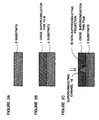
- FIG. 1A and 1B there are shown diagrammatic sectional views of two embodiments of the superconducting devices in accordance with the present invention.
- elements similar to each other are given the same Reference Numerals.
- the superconducting device shown in Figure 1 includes an oxide superconductor thin film 1 formed on a substrate 5 and having a non-superconducting region 50 which is formed by diffusion of constituent element(s) into the oxide superconductor thin film and which no longer has superconductivity.
- the oxide superconductor thin film forms a superconducting channel 10 of about five nanometers in thickness at a position above the non-superconducting region 50.
- an extremely thin gate electrode 4 is provided through a gate insulator layer 6.
- a source electrode 2 and a drain electrode 3 are located on the oxide superconductor thin film 1 at opposite sides of the superconducting channel 10, respectively.
- the gate electrode 4 is formed of a normal conductor thin film or an oxide superconductor thin film, and is deposited on a side surface of a surface protection layer 8 formed on the gate insulator 6.
- the normal conductor thin film can be deposited on the side surface of the surface protection layer 8 by for example an inclined evaporation process.
- the oxide superconductor thin film can be deposited on the side surface of the surface protection layer 8 by for example an off-axis sputtering. As seen from the drawing, the thin film of the gate electrode 4 stands upright on the gate insulator, and therefore, the thickness of the thin film of the gate electrode 4 determines a gate length.
- the embodiment shown in Figure 1B is different from the embodiment shown in Figure 1A, only in that the non-superconducting region 50 is constituted of a projection previously formed on the substrate 5.
- the other features of the embodiment shown in Figure 1B are completely the same as those of the embodiment shown in Figure 1A, and therefore, further explanation will be omitted.
- a substrate 5 is prepared as shown in Figure 2A.
- Thid substrate 5 is formed of for example, an insulating substrate such as a MgO (100) substrate, a SrTiO3 (100) substrate or others, or a semiconductor substrate such as a silicon (100) substrate having a principal surface coated with insulating films.
- an insulating substrate such as a MgO (100) substrate, a SrTiO3 (100) substrate or others
- a semiconductor substrate such as a silicon (100) substrate having a principal surface coated with insulating films.
- a principal surface of the silicon substrate is continuously coated with MgAl2O4 by a CVD process and with BaTiO3 by a sputtering process.
- an oxide superconductor thin film 1 having a thickness on the order of 200nm to 300nm is deposited on the substrate 5, by for example an off-axis sputtering, a reactive evaporation, an MBE (molecular beam epitaxy), a CVD, etc.
- the oxide superconductor material is preferably formed of, for example, a Y-Ba-Cu-O type compound oxide superconductor material, a Bi-Sr-Ca-Cu-O type compound oxide superconductor material, and a Tl-Ba-Ca-Cu-O type compound oxide superconductor material.
- the oxide superconductor thin film is preferably formed of a c -axis orientated oxide superconductor thin film, since the c -axis orientated oxide superconductor thin film has a large critical current density in a direction parallel to the substrate.
- the c -axis oriented oxide superconductor thin film can be formed by maintaining the substrate temperature at about 700°C in a film deposition process.
- a laser beam or a focused ion beam is locally irradiated onto the oxide superconductor thin film 1, as shown by arrows in Figure 2C, so that constituent element(s) of the substrate 5 is caused to diffuse into the oxide superconductor thin film 1 so as to form the non-superconducting region 50.
- a portion of the oxide superconductor thin film remaining above the non-superconducting region 50 forms the superconducting channel 10.
- a high power laser beam such as an excimer laser, a CO2 laser, a YAG laser, etc.
- a high power laser beam such as an excimer laser, a CO2 laser, a YAG laser, etc.
- an Ar laser having a wavelenght of 514nm it is preferred to scan the laser beam having an irradiation output power of 2.0W at a speed of 100 ⁇ m/second.
- Ar irradiation output power of 2.0W at a speed of 100 ⁇ m/second.
- an focused ion beam is locally irradiated onto the substrate 5 so as to form a doped region 51.
- the irradiated ions preferably are Ba ions, Y ions, or Cu ions.
- the beam diameter is 0.2 ⁇ m and the acceleration voltage is 50KV.
- the doped region 51 having a width of not greater than 1 ⁇ m is formed on the principal surface of the substrate 5 by irradiation of the focused ion beam.
- the oxide superconductor thin film 1 is deposited on the substrate 5 having the doped region 51, by for example the off-axis sputtering, the reactive evaporation, the MBE, the CVD, etc., similarly to the process of Figure 2C.
- doped elements are diffused from the doped region 51 into the oxide superconductor thin film 1 so as to form the non-superconducting region 50.
- a superconducting portion of the oxide superconductor thin film remaining above the non-superconducting region 50 forms the superconducting channel 10.
- an insulator film 16 is formed on the oxide superconductor thin film 1, and then, surface protection insulating layers 8 and 9 are formed on the insulator film 16, excluding a limited region above the superconducting channel 10.
- the insulating layer 16 is preferably formed of an insulating material such as MgO, which does not form a large density of energy levels between the superconductor thin film 1 and the insulating layer 16.
- the insulating layer 16 has a thickness sufficient to prevent a tunnel current, for example, a thickness of not less than 10 nanometers.
- the surface protection insulating layers 8 and 9 preferably formed of MgO.
- a normal conductor film 18 is formed on the surface protection layer 8 by performing an evaporation in an inclined direction so as to ensure that the normal conductor film 18 is deposited on a side surface 8A of the surface protection layer 8 positioned above the superconducting channel 10.
- another normal conductor film 19 is simultaneously formed on the surface protection layer 9.
- these normal conductor films 18 and 19 are preferably formed of a refractory metal such as Ti, W, etc., or Au, or a silicide thereof.
- an anisotropic etching is conducted on the normal conductor films 18 and 19 by means of a reactive ion etching, or an Ar-ion milling, so that a portion of the normal conductor film 18 remains only on the side surface 8A of of the surface protection layer 8.
- This remaining normal conductor film 18 forms a gate electrode 4.
- This gate electrode 4 is preferred to have a thickness of not greater than 100nm.
- the insulator film 16 and the surface protection layers 8 and 9 are removed from opposite end regions of the oxide superconductor thin film 1. Therefore, the insulator film 16 remaining above the superconducting channel 10 forms a gate insulator layer 6.
- a source electrode 2 and a drain electrode 3 are formed on the opposite exposed end regions of the oxide superconductor thin film 1. The source electrode 2 and the drain electrode 3 are formed of the same normal conductor material as that of the gate electrode. Thus, the superconducting channel-FET is completed.
- the non-superconducting region 50 is formed by diffusing the constituent element(s) of the substrate into the oxide superconductor thin film 1.
- the present invention is not limited to this method.
- the substrate is previously machined or etched so as to have a projection corresponding to the non-superconducting region 50, and then, the oxide superconductor thin film 1 is deposited on the substrate surface having the projection, and thereafter, is planarized so that the oxide superconductor thin film 1 has an flat upper surface.
- the gate electrode is formed of a normal conductor, but can be formed of an oxide superconductor.
- an oxide superconductor thin film which has a thickness of not greater than 100nm and which is preferably an ⁇ -axis oriented film, is deposited, and then, the Ar-ion milling and the anisotropic etching are performed in an inclined direction so as to shape a superconducting gate electrode. Thereafter, the protection layers 8 and 9 are formed.
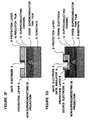
- FIG. 3K there are shown diagrammatic sectional views of a second embodiment of the superconducting device in accordance with the present invention.
- elements similar to those shown in Figures 1A to 2G are given the same Reference Numerals.
- the superconducting device shown in Figure 3K includes a gate insulator layer 6 and an oxide superconductor thin film 1 formed in the named order on a substrate 5 having a superconducting gate electrode 4 embedded therein.
- a surface protection layer 7 is formed on a portion of the oxide superconductor thin film 1 above the superconducting gate electrode 4.
- a source electrode 2 and a drain electrode 3 are formed on the oxide superconductor thin film 1 at both sides of the surface protection layer 7, respectively.
- the oxide superconductor thin film 1 is formed of a ⁇ -axis oriented oxide superconductor crystal layer having a thickness of not greater than about five nanometers, so that a portion of the oxide superconductor thin film 1 above the embedded superconducting gate electrode 4 forms the superconducting channel 10.
- the gate insulator layer 6 is preferably formed of an insulating material such as MgO, Si3N4, and has a thickness sufficient to prevent a tunnel current, for example, a thickness of not less than 10 nanometers.
- the superconducting gate electrode 4 is formed of an a -axis oriented oxide superconductor crystal layer and has a thickness of not greater than about 100nm in a direction of an electric current flowing through the superconducting channel 10.
- a substrate 5 is prepared as shown in Figure 3A.
- this substrate 5 is formed of for example, an insulating substrate such as a MgO (100) substrate, a SrTiO3 (100) substrate or others, or a semiconductor substrate such as a silicon (100) substrate having a principal surface coated with an insulating film.
- an insulating substrate such as a MgO (100) substrate, a SrTiO3 (100) substrate or others
- a semiconductor substrate such as a silicon (100) substrate having a principal surface coated with an insulating film.
- the silicon substrate is coated with an insulating film after a step explained hereinafter is formed.
- a photoresist 20 is deposited and patterned to cover a portion 5A of the substrate, and then, an uncovered portion of the substrate 5 is etched by a dry etching such as a reactive ion etching and an Ar-ion milling, so that a step 53 is formed as shown in Figure 3C. Thereafter, the photoresist 20 is removed.
- a dry etching such as a reactive ion etching and an Ar-ion milling
- a crystalline direction is important, and therefore, the process is modified.
- a photoresist mask 20 is formed so as to ensure that a gate length direction (a channel current direction) is perpendicular to a Si(110) plane.
- the silicon substrate partially masked with the photoresist 20 is etched with an etching liquid such as KOH or APW, so that a step 53 is formed as shown in Figure 3C.
- the principal surface having the step 53 is continuously coated with MgAlO4 by a CVD (chemical vapor deposition) and with BaTiO3 by a sputtering process.
- an ⁇ -axis oxide superconductor thin film 11 having thickness of not greater than 100nm is deposited on the principal surface of the substrate 5 at a substrate temperature of not greater than 650°C, by for example an off-axis sputtering, a reactive evaporation, an MBE (molecular beam epitaxy), a CVD, etc.
- the oxide superconductor material is preferably formed of, for example, a Y-Ba-Cu-O type compound oxide superconductor material, a Bi-Sr-Ca-Cu-O type compound oxide superconductor material, and a Tl-Ba-Ca-Cu-O type compound oxide superconductor material.
- the ⁇ -axis oriented thin film has a large critical current density in a direction perpendicular to the substrate surface.
- the oxide superconductor thin film 11 is selectively removed from a projected portion 5A and a recessed portion 5B of the substrate surface by an anisotropic etching such as a reactive ion etching, so that a superconducting gate electrode 4 is formed on only a side surface of the step 53 as shown in Figure 3E.
- the same material as that of the substrate 5 is deposited by sputtering so that a layer 54 having a thickness sufficient to perfectly fill the recessed portion 5B, as shown in Figure 3F.
- a photoresist (not shown) is deposited to cover the layer 54 and to have a flat upper surface. Thereafter, as shown in Figure 3G, the photoresist on the layer 50 and the layer 50 itself are etched backed and planarized by the Ar-ion etching until an upper end of the superconducting gate electrode 4 is exposed.
- a gate insulator layer 6 is formed on the planarized surface of the substrate 5.
- This gate insulator layer 6 is preferably formed of an insulating material such as MgO, which does not form a large density of energy levels between the oxide superconductor thin film and the gate insulator layer 6.
- the gate insulator layer 6 has a thickness sufficient to prevent a tunnel current, for example, a thickness of not less than 10 nanometers.
- a c -axis oxide superconductor thin film 1 having a thickness of not greater than five nanometers is deposited on the gate insulator layer 6.
- This c -axis oxide superconductor thin film 1 can be formed at a substrate temperature of about 700°C, by for example an off-axis sputtering, a reactive evaporation, the MBE, the CVD, ect.
- the c -axis orientated thin film has a large critical current density in a direction in parallel to the substrate surface.
- a surface protection layer 17 is deposited to cover the whole of the oxide superconductor thin film 1. Thereafter, the surface protection layer 17 is selectively removed so that the surface protection layer 17 remains only above the superconducting gate electrode 4.
- a source electrode 2 and a drain electrode 3 are formed on the oxide superconductor thin film 1 at both sides of the remaining surface protection layer 7.
- the source electrode 2 and the drain electrode 3 are formed of a normal conductor, for example, a refratory metal such as Ti, W, etc., or Au, or a silicide thereof, or an oxide superconducting material.
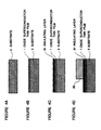
- FIG. 4L there are shown diagrammatic sectional views of a third embodiment of the superconducting device in accordance with the present invention.
- elements similar to those shown in Figures 1A to 3K are given the same Reference Numerals.
- the superconducting device shown in Figure 4L includes an oxide superconductor thin film 1 deposited on a substrate 5 so as to form a superconducting channel.
- An insulating layer 61 is formed on the oxide superconductor thin film 1 above the superconducting gate electrode 4.
- a superconducting source electrode 2 and a superconducting drain electrode 3 are formed on both end portions of the insulating layer 61, respectively.
- the substrate 5 is formed of for example, an insulating substrate such as a MgO (100) substrate, a SrTiO3 (100) substrate, a CdNdAlO4 (100) substrate or others.
- the oxide superconductor thin film 1 is formed of a c -axis oriented oxide superconductor crystal layer having a thickness of not greater than about five nonometers, and on the other hand, the superconducting source electrode 2 and the superconducting drain electrode 3 are formed of a ⁇ -axis oriented oxide superconductor crystal layer having a thickness of about 200nm.
- the superconducting gate electrode 4 is similarly formed of an ⁇ -axis oriented oxide superconductor crystal layer and has a thickness of not greater than about 100nm in a direction in parallel to the oxide superconductor thin film 1.
- the insulating layer 77 surrounding the superconducting gate electrode 4 is preferably formed of an insulating material such as MgO, Si3N4, and has a thickness sufficient to prevent a tunnel current, for example, a thickness of not less than 10 nanometers.
- the insulating layer 61 is formed of a MgO film having a thickness of not greater than 10 nanometers. In a portion of the insulating layer 61 under each of the superconducting source electrode 2 and the superconducting drain electrode 3, MgO flocculates so that the oxide superconductor thin film 1 is in electric connection with the superconducting source electrode 2 and the superconducting drain electrode 3, respectively.
- a substrate 5 is prepared as shown in Figure 4A.
- this substrate 5 is formed of for example, an insulating substrate such as a MgO (100) substrate, a SrTiO3 (100) substrate or others, or a semiconductor substrate such as a silicon (100) substrate having a principal surface coated with an insulating film.
- an insulating substrate such as a MgO (100) substrate, a SrTiO3 (100) substrate or others
- a semiconductor substrate such as a silicon (100) substrate having a principal surface coated with an insulating film.
- a principal surface of the silicon substrate is continuously coated with MgAl2O4 by a CVD process and with BaTiO3 by a sputtering process.
- a c -axis oxide superconductor thin film 1 having a thickness of not greater than five nanometers is deposited on the substrate 5.
- This c -axis oxide superconductor thin film 1 can be formed by for example an off-axis sputtering, a reactive evaporation, the MBE, the CVD, etc.
- the c -axis orientated thin film has a large critical current density in a direction in parallel to the substrate surface.
- an insulating layer 61 is formed on the oxide superconductor thin film 1, as shown in Figure 4C.
- the thickness of the insulating layer 61 is made to be not greater than ten nanometers.
- the insulating layer 61 is formed of an insulating material such as MgO, which can realize an electric connection due to flocculation.
- a sublimation type resist layer 80 of for example Mo is formed on a right half (in the drawing) of the insulating layer 61, by a vacuum evaporation process.
- an ⁇ -axis oxide superconductor thin film having a thickness of about 200nm is deposited on a portion of the insulating layer 61 which is not covered by the resist layer 80, so that a superconducting source electrode 2 is formed.
- This ⁇ -axis oxide superconductor thin film can be formed by for example an off-axis sputtering, a reactive evaporation, the MBE, the CVD, etc., and at a substrate temperature of not greater than 650°C.
- the sublimation type resist layer 80 sublimates, so that the right half of the insulating layer 61 is exposed.
- an insulating layer 70 such as MgO or Si3N4 is deposited to continuously and uniformly cover the superconducting source electrode 2 and the insulating layer 61.
- the insulating layer 70 cooperates with the insulating layer 61 so as to form a gate insulator layer, and therefore, the insulating layer 70 is made to have a thickness of not greater than ten nanometers in order to prevent a tunnel current.
- an oxide superconductor thin film 14 is deposited on the insulating layer 70.
- This oxide superconductor thin film 14 is formed of an ⁇ -axis oriented oxide superconductor crystal layer having a thickness of not greater than about 100nm.
- This oxide superconductor thin film 14 can be formed by an off-axis sputtering similarly to the superconducting source electrode 2 by maintaining the substrate temperature not greater than 650°C.
- the oxide superconductor thin film 14 and the insulating layer 70 are anisotropically etched by a reactive ion etching, an Ar-ion milling or other suitable means, so that the oxide superconductor thin film 14 and the insulating layer 70 are left on only a side surface of the superconducting source electrode 2.
- the remaining superconductor thin film 14 forms a superconducting gate electrode 4.
- an etching is performed so that the right half portion of the insulating layer 61 is exposed again.
- an insulating layer 72 is deposited to continuously and uniformly cover the superconducting source electrode 2, the remaining insulating layer 70, the superconducting gate electrode 4 and an exposed surface of the insulating layer 61.
- the insulating layer 72 is formed of the same material as that of the insulating layer 70.
- the insulating layer 70 is anisotropically etched by a reactive ion etching, an Ar-ion milling or other suitable means, so as to finish the superconducting gate electrode 4 surrounded by the insulating layer 77.
- An etching is performed so that the right half portion of the insulating layer 61 is exposed again.
- an oxide superconductor thin film 13 is deposited to continuously and uniformly cover the superconducting source electrode 2, the insulating layer 77, the superconducting gate electrode 4 and an exposed surface of the insulating layer 61.
- This oxide superconductor thin film 13 is formed of an ⁇ -axis oriented oxide superconductor crystal layer having a thickness of not greater than about 200nm.
- This oxide superconductor thin film 13 can be formed by an off-axis sputtering similarly to the superconducting gate electrode 4 by maintaining the substrate temperature not greater than 650°C.
- MgO flocculates At a boundary between the insulating layer 61 and the oxide superconductor thin film 13, MgO flocculates, so that an electrical connection is formed between the oxide superconductor thin film 1 and the oxide superconductor thin film 13.
- a photoresist is deposited to cover the oxide superconductor thin film 13 and to have a flat upper surface, and etched back and planarized until the upper end surface of the superconducting gate electrode 4 is exposed as shown in Figure 4L.
- the superconducting device in accordance with the present invention a main current flows through the superconducting channel and is controlled by the gate voltage. Therefore, differently from the conventional super-FET in which a superconducting current flows through the semiconductor channel due to the superconducting proximity effect, the fine processing techniques which had been required for manufacturing the super-FET have become unnecessary. In addition, since it is not necessary to stack the superconductor and the semiconductor, high performance superconducting device can be realized by using an oxide superconductor. Furthermore, since the gate length can be shortened, the superconducting device in accordance with the present invention can operate at a high speed. Therefore, the application of the superconduction technology to the electronic devices can be promoted.
Landscapes
- Superconductor Devices And Manufacturing Methods Thereof (AREA)
Applications Claiming Priority (6)
| Application Number | Priority Date | Filing Date | Title |
|---|---|---|---|
| JP294287/90 | 1990-10-31 | ||
| JP294288/90 | 1990-10-31 | ||
| JP2294287A JP2614941B2 (ja) | 1990-10-31 | 1990-10-31 | 超電導素子および作製方法 |
| JP294289/90 | 1990-10-31 | ||
| JP2294289A JP2599499B2 (ja) | 1990-10-31 | 1990-10-31 | 超電導素子および作製方法 |
| JP2294288A JP2738144B2 (ja) | 1990-10-31 | 1990-10-31 | 超電導素子および作製方法 |
Publications (3)
| Publication Number | Publication Date |
|---|---|
| EP0484251A2 true EP0484251A2 (de) | 1992-05-06 |
| EP0484251A3 EP0484251A3 (en) | 1992-08-19 |
| EP0484251B1 EP0484251B1 (de) | 1996-03-20 |
Family
ID=27337898
Family Applications (1)
| Application Number | Title | Priority Date | Filing Date |
|---|---|---|---|
| EP91402934A Expired - Lifetime EP0484251B1 (de) | 1990-10-31 | 1991-10-31 | Aus extrem dünnem supraleitendem Oxydfilm gebildete supraleitende Einrichtung mit extrem kurzem Kanal und Verfahren zu dessen Herstellung |
Country Status (4)
| Country | Link |
|---|---|
| US (2) | US5471069A (de) |
| EP (1) | EP0484251B1 (de) |
| CA (1) | CA2054644C (de) |
| DE (1) | DE69118106T2 (de) |
Cited By (3)
| Publication number | Priority date | Publication date | Assignee | Title |
|---|---|---|---|---|
| EP0576363B1 (de) * | 1992-06-24 | 1998-01-07 | Sumitomo Electric Industries, Ltd. | Verfahren zur Herstellung einer supraleitenden Einrichtung mit einem supraleitenden Kanal aus oxidisch supraleitendem Material |
| US5846846A (en) * | 1994-11-28 | 1998-12-08 | Electronics And Telecommunications Research Institute | Method for making a superconducting field-effect device with grain boundary channel |
| EP0825656A3 (de) * | 1996-08-13 | 1999-05-19 | Sumitomo Electric Industries, Limited | Supraleitende Schichtstruktur mit einer supraleitenden Oxyddünnschicht mit Schutzschicht und Verfahren zu deren Herstellung |
Families Citing this family (5)
| Publication number | Priority date | Publication date | Assignee | Title |
|---|---|---|---|---|
| US5908813A (en) * | 1997-02-14 | 1999-06-01 | Micron Technology, Inc. | Method making integrated circuit metallization with superconductor BEOL wiring |
| JPH1140867A (ja) * | 1997-07-22 | 1999-02-12 | Sumitomo Electric Ind Ltd | 超電導電界効果型素子およびその作製方法 |
| US6885781B2 (en) * | 2002-05-03 | 2005-04-26 | Fujitsu Limited | Thin film electro-optical deflector device and a method of fabrication of such a device |
| US7186380B2 (en) * | 2002-07-01 | 2007-03-06 | Hewlett-Packard Development Company, L.P. | Transistor and sensors made from molecular materials with electric dipoles |
| US9741918B2 (en) | 2013-10-07 | 2017-08-22 | Hypres, Inc. | Method for increasing the integration level of superconducting electronics circuits, and a resulting circuit |
Family Cites Families (8)
| Publication number | Priority date | Publication date | Assignee | Title |
|---|---|---|---|---|
| KR910002311B1 (ko) * | 1987-02-27 | 1991-04-11 | 가부시기가이샤 히다찌세이사꾸쇼 | 초전도 디바이스 |
| DE3876228T2 (de) * | 1988-01-15 | 1993-06-03 | Ibm | Feldeffektanordnung mit supraleitendem kanal. |
| JP2862137B2 (ja) * | 1988-08-11 | 1999-02-24 | 古河電気工業株式会社 | 超電導トランジスタ |
| JPH02194665A (ja) * | 1989-01-24 | 1990-08-01 | Fujitsu Ltd | 電界効果型超伝導装置及びその製造方法 |
| DE69123415T2 (de) * | 1990-09-06 | 1997-05-22 | Sumitomo Electric Industries | Supraleitendes Bauelement mit verringerter Dicke der supraleitenden Oxydschicht und dessen Herstellungsverfahren |
| CA2054477C (en) * | 1990-10-29 | 1996-12-24 | Takao Nakamura | Superconducting device having an extremely short superconducting channel formed of oxide superconductor material and method for manufacturing the same |
| CA2054795C (en) * | 1990-11-01 | 1996-08-06 | Hiroshi Inada | Superconducting device having an extremely thin superconducting channel formed of oxide superconductor material and method for manufacturing the same |
| EP0545801B1 (de) * | 1991-11-30 | 1997-03-19 | Sumitomo Electric Industries, Ltd. | Supraleitendes Bauelement mit extrem dünnen supraleitenden Kanal und Herstellungsverfahren |
-
1991
- 1991-10-31 DE DE69118106T patent/DE69118106T2/de not_active Expired - Fee Related
- 1991-10-31 EP EP91402934A patent/EP0484251B1/de not_active Expired - Lifetime
- 1991-10-31 CA CA002054644A patent/CA2054644C/en not_active Expired - Fee Related
-
1994
- 1994-05-13 US US08/242,074 patent/US5471069A/en not_active Expired - Fee Related
-
1995
- 1995-08-23 US US08/518,493 patent/US5637555A/en not_active Expired - Fee Related
Cited By (3)
| Publication number | Priority date | Publication date | Assignee | Title |
|---|---|---|---|---|
| EP0576363B1 (de) * | 1992-06-24 | 1998-01-07 | Sumitomo Electric Industries, Ltd. | Verfahren zur Herstellung einer supraleitenden Einrichtung mit einem supraleitenden Kanal aus oxidisch supraleitendem Material |
| US5846846A (en) * | 1994-11-28 | 1998-12-08 | Electronics And Telecommunications Research Institute | Method for making a superconducting field-effect device with grain boundary channel |
| EP0825656A3 (de) * | 1996-08-13 | 1999-05-19 | Sumitomo Electric Industries, Limited | Supraleitende Schichtstruktur mit einer supraleitenden Oxyddünnschicht mit Schutzschicht und Verfahren zu deren Herstellung |
Also Published As
| Publication number | Publication date |
|---|---|
| CA2054644C (en) | 1998-03-31 |
| DE69118106D1 (de) | 1996-04-25 |
| DE69118106T2 (de) | 1996-10-31 |
| EP0484251B1 (de) | 1996-03-20 |
| CA2054644A1 (en) | 1992-05-01 |
| EP0484251A3 (en) | 1992-08-19 |
| US5471069A (en) | 1995-11-28 |
| US5637555A (en) | 1997-06-10 |
Similar Documents
| Publication | Publication Date | Title |
|---|---|---|
| EP0480814B1 (de) | Supraleitende Einrichtung mit ultradünnem Kanal aus oxydisch supraleitendem Material und Verfahren zu deren Herstellung | |
| EP0478465B1 (de) | Verfahren zur Herstellung eines Supraleitungsbauelements mit reduzierter Dicke der supraleitenden Oxidschicht und dadurch hergestelltes Supraleitungsbauelement | |
| EP0484253B1 (de) | Supraleitende Einrichtung mit extrem dünnen supraleitenden Kanal aus oxydischem supraleitendem Material und Methode zu deren Herstellung | |
| EP0478464B1 (de) | Herstellungsverfahren eines supraleitenden Bauelements mit extrem dünnem supraleitenden Kanal aus supraleitendem Oxidmaterial | |
| EP0484251B1 (de) | Aus extrem dünnem supraleitendem Oxydfilm gebildete supraleitende Einrichtung mit extrem kurzem Kanal und Verfahren zu dessen Herstellung | |
| EP0475838B1 (de) | Supraleitende Einrichtung mit einer reduzierten Dicke der supraleitenden Schicht und Methode zu deren Herstellung | |
| EP0478466B1 (de) | Supraleitendes Bauelement und dessen Herstellungsverfahren | |
| EP0477103B1 (de) | Verfahren zur Herstellung einer supraleitenden Einrichtung mit reduzierter Dicke der supraleitenden Schicht und dadurch hergestellte supraleitende Einrichtung | |
| US5714767A (en) | Method for manufacturing superconducting device having a reduced thickness of oxide superconducting layer and superconducting device manufactured thereby | |
| EP0477063B1 (de) | Supraleitendes Bauelement mit verringerter Dicke der supraleitenden Oxydschicht und dessen Herstellungsverfahren | |
| US5854493A (en) | Superconduting device having an extremely short superconducting channel formed of oxide superconductor material and method for manufacturing the same | |
| EP0484252B1 (de) | Supraleitende Einrichtung aus oxydisch supraleitendem Material | |
| EP0534811A2 (de) | Verfahren zur Herstellung von supraleitenden Schichten aus supraleitendem Oxyd in denen nicht-supraleitende Gebiete vorkommen und Verfahren zur Herstellung eines Bauelements welches solche Schichten enthält | |
| EP0478463B1 (de) | Supraleitendes Bauelement mit extrem dünnem supraleitenden Kanal aus supraleitendem Oxidmaterial | |
| JP2641969B2 (ja) | 超電導素子および作製方法 | |
| JP2614941B2 (ja) | 超電導素子および作製方法 | |
| JP2641970B2 (ja) | 超電導素子および作製方法 |
Legal Events
| Date | Code | Title | Description |
|---|---|---|---|
| PUAI | Public reference made under article 153(3) epc to a published international application that has entered the european phase |
Free format text: ORIGINAL CODE: 0009012 |
|
| AK | Designated contracting states |
Kind code of ref document: A2 Designated state(s): DE FR GB |
|
| PUAL | Search report despatched |
Free format text: ORIGINAL CODE: 0009013 |
|
| AK | Designated contracting states |
Kind code of ref document: A3 Designated state(s): DE FR GB |
|
| 17P | Request for examination filed |
Effective date: 19920831 |
|
| 17Q | First examination report despatched |
Effective date: 19940823 |
|
| GRAA | (expected) grant |
Free format text: ORIGINAL CODE: 0009210 |
|
| AK | Designated contracting states |
Kind code of ref document: B1 Designated state(s): DE FR GB |
|
| REF | Corresponds to: |
Ref document number: 69118106 Country of ref document: DE Date of ref document: 19960425 |
|
| ET | Fr: translation filed | ||
| PLBE | No opposition filed within time limit |
Free format text: ORIGINAL CODE: 0009261 |
|
| STAA | Information on the status of an ep patent application or granted ep patent |
Free format text: STATUS: NO OPPOSITION FILED WITHIN TIME LIMIT |
|
| 26N | No opposition filed | ||
| PGFP | Annual fee paid to national office [announced via postgrant information from national office to epo] |
Ref country code: FR Payment date: 19971009 Year of fee payment: 7 |
|
| PGFP | Annual fee paid to national office [announced via postgrant information from national office to epo] |
Ref country code: GB Payment date: 19971022 Year of fee payment: 7 |
|
| PGFP | Annual fee paid to national office [announced via postgrant information from national office to epo] |
Ref country code: DE Payment date: 19971110 Year of fee payment: 7 |
|
| PG25 | Lapsed in a contracting state [announced via postgrant information from national office to epo] |
Ref country code: GB Free format text: LAPSE BECAUSE OF NON-PAYMENT OF DUE FEES Effective date: 19981031 |
|
| GBPC | Gb: european patent ceased through non-payment of renewal fee |
Effective date: 19981031 |
|
| PG25 | Lapsed in a contracting state [announced via postgrant information from national office to epo] |
Ref country code: FR Free format text: LAPSE BECAUSE OF NON-PAYMENT OF DUE FEES Effective date: 19990630 |
|
| REG | Reference to a national code |
Ref country code: FR Ref legal event code: ST |
|
| PG25 | Lapsed in a contracting state [announced via postgrant information from national office to epo] |
Ref country code: DE Free format text: LAPSE BECAUSE OF NON-PAYMENT OF DUE FEES Effective date: 19990803 |