EP0484232A2 - Supraleitende Einrichtung mit extrem kurzer supraleitender Kanallänge aus oxydisch supraleitendem Material und Verfahren zu deren Herstellung - Google Patents
Supraleitende Einrichtung mit extrem kurzer supraleitender Kanallänge aus oxydisch supraleitendem Material und Verfahren zu deren Herstellung Download PDFInfo
- Publication number
- EP0484232A2 EP0484232A2 EP91402900A EP91402900A EP0484232A2 EP 0484232 A2 EP0484232 A2 EP 0484232A2 EP 91402900 A EP91402900 A EP 91402900A EP 91402900 A EP91402900 A EP 91402900A EP 0484232 A2 EP0484232 A2 EP 0484232A2
- Authority
- EP
- European Patent Office
- Prior art keywords
- superconducting
- thin film
- oxide
- substrate
- oxide superconductor
- Prior art date
- Legal status (The legal status is an assumption and is not a legal conclusion. Google has not performed a legal analysis and makes no representation as to the accuracy of the status listed.)
- Granted
Links
Images


Classifications
-
- H—ELECTRICITY
- H10—SEMICONDUCTOR DEVICES; ELECTRIC SOLID-STATE DEVICES NOT OTHERWISE PROVIDED FOR
- H10N—ELECTRIC SOLID-STATE DEVICES NOT OTHERWISE PROVIDED FOR
- H10N60/00—Superconducting devices
- H10N60/20—Permanent superconducting devices
- H10N60/205—Permanent superconducting devices having three or more electrodes, e.g. transistor-like structures
- H10N60/207—Field effect devices
-
- Y—GENERAL TAGGING OF NEW TECHNOLOGICAL DEVELOPMENTS; GENERAL TAGGING OF CROSS-SECTIONAL TECHNOLOGIES SPANNING OVER SEVERAL SECTIONS OF THE IPC; TECHNICAL SUBJECTS COVERED BY FORMER USPC CROSS-REFERENCE ART COLLECTIONS [XRACs] AND DIGESTS
- Y10—TECHNICAL SUBJECTS COVERED BY FORMER USPC
- Y10S—TECHNICAL SUBJECTS COVERED BY FORMER USPC CROSS-REFERENCE ART COLLECTIONS [XRACs] AND DIGESTS
- Y10S505/00—Superconductor technology: apparatus, material, process
- Y10S505/825—Apparatus per se, device per se, or process of making or operating same
- Y10S505/873—Active solid-state device
Definitions
- the present invention relates to a superconducting device and a method for manufacturing the same, and more specifically to a superconducting device including an extremely short superconducting channel formed of oxide superconductor material, and a method for manufacturing the same.
- Typical three-terminal devices which utilize a superconductor include a so called superconducting-base transistor and a so called super-FET (field effect transistor).
- the superconducting-base transistor includes an emitter of a superconductor or a normal conductor, a tunnel barrier of an insulator, a base of a superconductor, a semiconductor isolator and a collector of a normal conductor, stacked in the named order.
- This superconducting-base transistor operates at a high speed with a low power consumption, by utilizing high speed electrons passing through the tunnel barrier.
- the super-FET includes a semiconductor layer, and a superconductor source electrode and a superconductor drain electrode which are formed closely to each other on the semiconductor layer.
- a portion of the semiconductor layer between the superconductor source electrode and the superconductor drain electrode has a greatly recessed or undercut war surface so as to have a reduced thickness.
- a gate electrode is formed through a gate insulating layer on the recessed or undercut rear surface of the portion of the semiconductor layer between the superconductor source electrode and the superconductor drain electrode.
- a superconducting current flows through the semiconductor layer portion between the superconductor source electrode and the superconductor drain electrode due to a proximity effect, and is controlled by an applied gate voltage.
- This super-FET also operates at a high speed with a low power consumption.
- Both of the above mentioned superconducting-base transistor and the super-FET have a portion in which a semiconductor layer and a superconducting layer are stacked to each other.
- the superconductor source electrode and the superconductor drain electrode have to be located close to each other at a distance which is not greater than a few times the coherence length of the superconductor materials of the superconductor source electrode and the superconductor drain electrode.
- the oxide superconductor has a short coherence length
- a distance between the superconductor source electrode and the superconductor drain electrode has to be not greater than a few ten nanometers.
- it is very difficult to conduct a fine processing such as a fine pattern etching so as to ensure the very short separation distance. Because of this, in the prior art, it has been impossible to manufacture the super-FET composed of the oxide superconductor material.
- the conventional three-terminal superconducting device having the superconducting channel shows a modulation operation.
- the conventional three-terminal superconducting device having the superconducting channel could not realize a complete ON/OFF operation, because a carrier density is too high.
- a thickness of the supeerconducting channel has to be made on the order of five nanometer or less.
- the operation speed of this device is determined by a gate length.
- this dimension of not greater than 0.1 ⁇ m by use of the conventional processing technique, and therefore, there has been a limit in speeding up the operation speed of the device.
- Another object of the present invention is to provide a superconducting device including a superconducting region constituted of an extremely thin oxide superconductor film, which can be manufactured by using existing established processing techniques with a good repeatability.
- Still another object of the present invention is to provide an FET type superconducting device including an extremely short superconducting channel composed of an oxide superconductor thin film, and a method for manufacturing the same with a good repeatability by using existing established processing techniques.
- a superconducting device comprising a substrate, a superconducting channel constituted of an oxide superconductor thin film formed to have an angle to a deposition surface of the substrate, a superconductor source electrode and a superconductor drain electrode formed at opposite ends of the superconducting channel, so that a superconducting current can flow through the superconducting channel between the superconductor source electrode and the superconductor drain electrode, and a gate electrode in the form of a sheet having an end abutted through an insulating layer on the superconducting channel so as to control the superconducting current flowing through the superconducting channel, the gate electrode being formed of an oxide superconductor thin film in parallel to the deposition surface of the substrate.
- the source electrode should be understood to include not only an electrode corresponding to the electrode which is called a "source electrode” in the field of a semiconductor MOSFET, but also a source region which is formed adjacent to and continuous to the superconducting channel and on which the source electrode is formed
- the drain electrode should be understood to include not only an electrode corresponding to the electrode which is called a “drain electrode” in the field of the semiconductor MOSFET, but also a drain region which is formed adjacent to and continuous to the superconducting channel and on which the drain electrode is formed.
- the angle of the oxide superconductor thin film of the superconducting channel to the deposition surface of the substrate is determined, in the range of greater than 0° but less than 180°, on the basis of the thickness of the oxide superconductor thin film constituting the gate electrode and the gate length to be obtained.
- this angle is preferably not less than 30° but not greater than 90°. Therefore, this angle should be 90° in order to obtain the shortest gate length in a given thickness of the oxide superconductor thin film constituting the gate electrode.
- a desired gate length can be obtained by controlling the thickness of the oxide superconductor thin film constituting the gate electrode.
- the superconducting device in accordance with the present invention is characterized in that the superconducting channel is constituted of the oxide superconductor thin film and formed to have some angle to the deposition surface of the substrate, and in that the gate electrode is formed of the oxide superconductor thin film in parallel to the deposition surface of the deposition surface of the substrate, so that an end of the oxide superconductor thin film of the gate electrode is in contact with the gate insulator so as to oppose through the insulating layer to the superconducting channel.
- the oxide superconductor thin film of the gate electrod can be formed to have a thickness of not greater than about 100nm.
- a gate length of the gate electrode is substantially determined by the thickness of the oxide superconductor thin film of the gate electrode.
- the super-FET in accordance with the present invention can have an extremely short superconducting channel which is controlled by the gate electrode, and accordingly, the current flowing through the superconducting channel can be turned on and off at a high speed.
- the superconducting device in accordance with the present invention can have the above mentioned shortened gate without using the fine-processing technique.
- a thickness of the superconducting channel has to be not greater than five nanometers in the direction of an electric field created by the voltage applied to the gate electrode. This extremely thin superconducting channel is realized in the superconducting device in accordance with the present invention.
- the superconducting device in accordance with the present invention is constructed so that a main current flows through the superconductor material. Therefore, the superconducting device in accordance with the present invention is not required to locate the pair of superconducting electrodes apart from each other by an extremely short distance.
- the shortened gate can be formed without using the fine-processing technique as mentioned above, and the superconducting channel can be also formed without using the fine-processing technique as will be explained hereinafter. Therefore, the limitation in the fine processing techniques required for manufacturing the super-FET can be relaxed.
- the above mentioned superconducting device in accordance with the present invention can be formed by the method in accordance with the present invention for manufacturing the superconducting device, which method includes the step of forming and stacking a first oxide superconducting thin film and a first insulating layer on an insulting surface of a substrate in the name order, partially removing the stacked structure of the first oxide superconducting thin film and the first insulting layer so as to have a smooth continuous end surface having an angle to the insulting surface of a substrate and extending from the first insulating layer at least to a bottom surface of the first oxide superconducting thin film, and forming and stacking a second insulting layer and a second oxide superconducting thin film in the name order on the end surface of the stacked structure of the first oxide superconducting thin film and the first insulting layer, so that the first oxide superconducting thin film functions as a gate electrode and the second insulating layer functions as a gate insulator and so that a first portion of the second oxide superconducting thin
- the first oxide superconducting thin film constituting the superconducting gate electrode is first formed on the substrate.
- a film of an insulator such as MgO can be formed on the substrate if necessary, and thereafter, the first oxide superconducting thin film can be formed on the insulator film.
- the first insulating layer is deposited on the first oxide superconducting thin film, and the stacked structure of the first oxide superconducting thin film and the first insulating layer is partially etched to have a smooth continuous end surface having an angle to the deposition surface of the substrate and extending from the first insulating layer at least to a bottom surface of the first oxide superconducting thin film.
- This etching can be performed by using, preferably, a scan type etching such as a focused ion beam etching.
- a second insulating layer constituting the gate insulator and the second oxide superconductor thin film constituting the superconducting channel are formed on the end surface of the stacked structure of the first oxide superconducting thin film and the first insulating layer.
- the oxide superconductor thin film constituting the superconducting channel has to have a thickness on the order of about five nanometers or less.
- Such an extremely thin oxide superconductor thin film can be formed in a conventional process by precisely controlling the growth speed and the growth time of the thin film. For this purpose, a sputtering can be used.
- the oxide superconductor crystal has a multi-layer structure in which respective constituent elements are stacked in a layered structure, it is possible to stack a desired number of units cells of oxide superconductor, by using a MBE (molecular beam epitaxy).
- MBE molecular beam epitaxy
- the oxide superconductor thin films is formed of a high-Tc (high critical temperature) oxide superconductor material.
- This high-Tc oxide superconductor material has been studied by many researchers since the discovery of Bednorz and Müller in 1986, and is said to indicate an oxide superconductor material having a critical temperature of not less than 30K.
- the oxide superconductor thin film is formed of a high-Tc copper-oxide type oxide superconductor material including a Y-Ba-Cu-O type compound oxide superconductor material, a Bi-Sr-Ca-Cu-O type compound oxide superconductor material, and a Tl-Ba-Ca-Cu-O the compound oxide superconductor material.
- the substrate, on which the oxide superconductor thin film is deposited can be formed of an insulating substrate, preferably an oxide single crystalline substrate such as MgO, SrTiO3, and CdNdAlO4. These substrate materials are very effective in forming or growing a crystalline film having a high orientation property.
- the superconducting device can be formed on a semiconductor substrate if an appropriate buffer layer is deposited thereon.
- the buffer layer on the semiconductor substrate can be formed of a double-layer coating formed of a MgAl2O4 layer and a BaTiO3 layer if a silicon substrate is used.
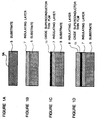
- a substrate 5 is prepared as shown in Figure 1A.
- This substrate 5 is formed of for example, an insulating substrate such as a MgO (100) substrate, a SrTiO3 (100) substrate or others, or a semiconductor substrate such as a silicon (100) substrate having a principal surface coated with insulating films.
- an insulating substrate such as a MgO (100) substrate, a SrTiO3 (100) substrate or others
- a semiconductor substrate such as a silicon (100) substrate having a principal surface coated with insulating films.
- a principal surface of the semiconductor substrate is continuously coated with MgAl2O4 by a CVD process and with BaTiO3 by a sputtering process.
- an insulating layer 7 such as a MgO and others is deposited on a principal surface or deposition surface 5A of the substrate 5 by a sputtering process, so as to have a thickness of about 200nm.
- the insulating layer 7 can be omitted.
- a c -axis oriented oxide superconductor thin film 11 which has a thickness of not greater than about 100nm and which will form a superconducting gate electrode, is deposited on the insulating layer 7, by for example an off-axis sputtering, a reactive evaporation, an MBE (molecular beam epitaxy), a CVD, etc.
- the oxide superconductor material is preferably formed of, for example, a Y-Ba-Cu-O type compound oxide superconductor material, a Bi-Sr-Ca-Cu-O type compound oxide superconductor material, and a Tl-Ba-Ca-Cu-O type compound oxide superconductor material.
- the c -axis orientated oxide superconductor thin film has a large critical current density in a direction parallel to the substrate.
- an insulating layer 8 such as a MgO and others is deposited on the principal surface of the oxide superconductor thin film 11 by a sputtering process, so as to have a thickness of about 300nm.
- the insulating layer 7, the oxide superconductor thin film 11 and the insulating layer 8 are continuously deposited without being taken out of a deposition chamber.
- an right portion (in the drawing) of a stacked structure of the insulating layer 7, the oxide superconductor thin film 11 and the insulating layer 8 is completely removed by an etching process, so that the stacked structure has a vertical end surface 15 extending from an upper surface of the insulating layer 8 to a bottom surface of the insulating layer 7, and a right portion of the substrate 5 is exposed.
- the end surface 15 is perpendicular to the principal surface or deposition surface 5A of the substrate 5.
- This etching is performed by using a scan type etching such as a focused ion beam etching.
- a gate insulator layer 6 is formed to cover the vertical end surface 15, an upper surface of the insulating layer 8, and the exposed surface of the substrate 5.
- the gate insulator layer 6 is formed of, for example, MgO, Si3N4, etc., and has a thickness sufficient to prevent a tunnel current, for example, a thickness of not less than 10 nanometers.
- an a-axis orientated oxide superconductor thin film 1 is deposited on the gate insulator layer 6 by an off-axis sputtering at a temperature of not greater than 650°C.
- This oxide superconductor thin film 1 is formed of the same oxide superconductor material as that of the oxide superconductor thin film 11 and has a thickness of not greater than 5nm.
- a portion of the oxide superconductor thin film 1 deposited above the upper surface of the insulating layer 8 and the exposed surface of the substrate 5 has the a -axis perpendicular to the principal surface or deposition surface 5A of the substrate 5, a portion of the oxide superconductor thin film 1 deposited above the vertical end surface 15 has the a -axis in parallel to the vertical end surface and therefore has a large critical current density in a direction parallel to the vertical end surface 15.
- a left end portion (in the drawing) of the oxide superconductor thin film 1, the gate insulator layer 6 and the insulating layer 8 is removed by a reactive ion etching or an Ar ion milling, so that a left end portion 14 of the superconducting gate electrode 11 is exposed.
- a gate electrode 4, a source electrode 2 and a drain electrode 3 are formed on the exposed left end portion 14 of the superconducting gate electrode 11, and opposite end portions of the the oxide superconductor thin film 1, respectively.
- These electrodes are preferably formed of a refractory metal such as Ti, W, etc., or Au, or a silicide thereof, by any appropriate process such as a vacuum evaporation process.
- a passivation film can be formed to cover these electrodes. With this, the super-FET is completed.
- the limitation in the fine processing technique required for manufacturing the super-FET is relaxed. Accordingly, it is easy to manufacture the super-FET with good repeatability, and the manufactured super-FET has a stable performance.
- the first embodiment of the super-FET in accordance with the present invention includes the superconducting gate electrode 11 of the oxide superconductor material stacked on the insulating layer formed on the substrate 5.
- the gate electrode 4 is formed on the left portion of the superconducting gate electrode 11.
- the superconducting gate electrode 11 has a right portion having an upper surface coated with the insulating layer 8, so that the insulating layer 7, the superconducting gate electrode 11 and the insulating layer 8 from the stacked structure.
- the stacked structure of the insulating layer 7, the superconducting gate electrode 11 and the insulating layer 8 has a single common right end surface 15 perpendicularly to the principal surface or deposition surface 5A of the substrate 5.
- the gate insulator layer 6 and the oxide superconductor thin film 1 are formed in the named order, and the gate insulator layer 6 and the oxide superconductor thin film 1 extend continuously to extend on the upper surface of the insulating layer 8 and the upper surface of the substrate 5.
- This superconducting channel 10 has a large critical current density along a current flowing direction within the superconducting channel 10, since as mentioned above the portion of the oxide superconductor thin film 1 deposited above the vertical end surface 15 has the a -axis in parallel to the vertical end surface and therefore has a large critical current density in a direction parallel to the vertical end surface 15.
- the source electrode 2 and the drain electrode 3 are formed on opposite end portions of the oxide superconductor thin film 1.
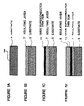
- an right portion (in the drawing) of a stacked structure of the insulating layer 7, the oxide superconductor thin film 11 and the insulating layer 8 is removed by an etching process so as to have a common single inclined end surface 15, and a right portion of the substrate 5 is exposed.
- This etching is performed by using a scan type etching such as a focused ion beam etching.
- a gate insulator layer 6 is formed to cover the inclined end surface 15, an upper surface of the insulating layer 8, and the exposed surface of the substrate 5.
- the gate insulator layer 6 is formed of, for example, MgO, Si3N4, etc., and has a thickness sufficient to prevent a tunnel current, for example, a thickness of not less than 10 nanometers.
- a c -axis oriented oxide superconductor thin film 1 is deposited on the gate insulator layer 6 by an off-axis sputtering at a temperature of about 700°C.
- This oxide superconductor thin film 1 is formed of the same oxide superconductor material as that of the oxide superconductor thin film 11 and has a thickness of not greater than 5nm.
- a portion of the oxide superconductor thin film 1 deposited above the inclined end surface 15 has the c -axis perpendicular to the inclined end surface and therefore has a large critical current density in a direction parallel to the inclined end surface 15.
- a left end portion (in the drawing) of the oxide superconductor thin film 1, the gate insulator layer 6 and the insulating layer 8 is removed by a reactive ion etching or an Ar ion milling, so that a left end portion 14 of the superconducting gate electrode 11 is exposed.
- a gate electrode 4, a source electrode 2 and a drain electrode 3 are formed on the exposed left end portion 14 of the superconducting gate electrode 11, and opposite end portions of the the oxide superconductor thin film 1, respectively.
- These electrodes are preferably formed of refractory metal such as Ti, W, etc., or Au, or a silicide thereof, by any appropriate process such as a vacuum evaporation process.
- a passivation film can be formed to cover these electrodes. With this, the super-FET is completed.
- limitation in the fine processing technique required for manufacturing the super-FET is also relaxed. Accordingly, it is easy to manufacture the super-FET with good repeatability, and the manufactured super-FET has a stable performance.
- the second embodiment of the super-FET in accordance with the present invention includes the superconducting gate electrode 11 of the oxide superconductor material stacked on the insulating layer 7 formed on the substrate 5.
- the gate electrode 4 is formed on the left portion of the superconducting gate electrode 11.
- the superconducting gate electrode 11 has the right portion having an upper surface coated with the insulating layer 8 so that the insulating layer 7, the superconducting gate electrode 11 and the insulating layer 8 form the stacked structure.
- the stacked structure of the insulating layer 7, the superconducting gate electrode 11 and the insulating layer 8 has a single common end surface 15 inclined to the principal surface or deposition surface 5A of the substrate 5.
- the gate insulator layer 6 and the oxide superconductor thin film 1 are formed in the named order so as to continuously extend on the upper surface of the insulating layer 8 and the upper surface of the substrate 5.
- This superconducting channel 10 has a large critical current density along a current flowing direction within the superconducting channel 10, since as mentioned above the portion of the oxide superconductor thin film 1 deposited above the inclined end surface 15 has the c -axis perpendicular to the inclined end surface and therefore has a large critical current density in a direction parallel to the inclined end surface 15.
- the source electrode 2 and the drain electrode 3 are formed on the opposite end portions of the oxide superconductor thin film 1.
- the oxide superconductor thin film 11 forming the superconducting gate electrode is deposited to have a thickness of 50nm.
- the angle of the inclined end surface 15 to the deposition surface 5A of the substrate 5 and the thickness of the oxide superconductor thin film 11 constituting the gate electrode is determined on the basis of the gate length to be obtained.
- the superconducting device in accordance with the present invention a main current flows through the superconducting channel and is controlled by the gate voltage. Therefore, differently from the conventional super-FET in which a superconducting current flows through the semiconductor channel due to the superconducting proximity effect, the fine processing techniques which had been required for manufacturing the super-FET have become unnecessary. In addition, since it is not necessary to stack the superconductor and the semiconductor, high performance superconducting device can be realized by using an oxide superconductor. Furthermore, since the gate length can be shortened, the superconducting devise in accordance with the present invention can operate at a high speed. Therefore, the application of the superconduction technology to the electronic devices can be promoted.
Landscapes
- Superconductor Devices And Manufacturing Methods Thereof (AREA)
Applications Claiming Priority (6)
| Application Number | Priority Date | Filing Date | Title |
|---|---|---|---|
| JP291198/90 | 1990-10-29 | ||
| JP29119890 | 1990-10-29 | ||
| JP291197/90 | 1990-10-29 | ||
| JP2291197A JP2614939B2 (ja) | 1990-10-29 | 1990-10-29 | 超電導素子および作製方法 |
| JP2291198A JP2614940B2 (ja) | 1990-10-29 | 1990-10-29 | 超電導素子および作製方法 |
| JP29119790 | 1990-10-29 |
Publications (4)
| Publication Number | Publication Date |
|---|---|
| EP0484232A2 true EP0484232A2 (de) | 1992-05-06 |
| EP0484232A3 EP0484232A3 (en) | 1992-08-12 |
| EP0484232B1 EP0484232B1 (de) | 1995-04-19 |
| EP0484232B2 EP0484232B2 (de) | 2001-10-10 |
Family
ID=26558442
Family Applications (1)
| Application Number | Title | Priority Date | Filing Date |
|---|---|---|---|
| EP91402900A Expired - Lifetime EP0484232B2 (de) | 1990-10-29 | 1991-10-29 | Supraleitende Einrichtung mit extrem kurzer supraleitender Kanallänge aus oxydisch supraleitendem Material und Verfahren zu deren Herstellung |
Country Status (4)
| Country | Link |
|---|---|
| US (1) | US5854493A (de) |
| EP (1) | EP0484232B2 (de) |
| CA (1) | CA2054477C (de) |
| DE (1) | DE69109054T3 (de) |
Cited By (3)
| Publication number | Priority date | Publication date | Assignee | Title |
|---|---|---|---|---|
| EP0484251A3 (en) * | 1990-10-31 | 1992-08-19 | Sumitomo Electric Industries, Ltd. | Superconducting device having an extremely short superconducting channel formed of extremely thin oxide superconductor film and method for manufacturing the same |
| US5750474A (en) * | 1995-12-15 | 1998-05-12 | Electronics And Telecommunications Research Institute | Method for manufacturing a superconductor-insulator-superconductor Josephson tunnel junction |
| US5846846A (en) * | 1994-11-28 | 1998-12-08 | Electronics And Telecommunications Research Institute | Method for making a superconducting field-effect device with grain boundary channel |
Families Citing this family (4)
| Publication number | Priority date | Publication date | Assignee | Title |
|---|---|---|---|---|
| JP2002266072A (ja) * | 2001-03-09 | 2002-09-18 | Sumitomo Electric Ind Ltd | 積層膜および成膜方法 |
| US20070254402A1 (en) * | 2006-04-27 | 2007-11-01 | Robert Rotzoll | Structure and fabrication of self-aligned high-performance organic fets |
| US10367134B2 (en) | 2017-06-07 | 2019-07-30 | International Business Machines Corporation | Shadow mask sidewall tunnel junction for quantum computing |
| FR3068518B1 (fr) * | 2017-06-28 | 2019-08-30 | Commissariat A L'energie Atomique Et Aux Energies Alternatives | Procede de controle d'un dispositif quantique a qubit de spin |
Family Cites Families (6)
| Publication number | Priority date | Publication date | Assignee | Title |
|---|---|---|---|---|
| JPS6117983A (ja) * | 1984-07-04 | 1986-01-25 | 日本原子力事業株式会社 | 原子炉緊急停止装置 |
| US4831421A (en) * | 1985-10-11 | 1989-05-16 | International Business Machines Corporation | Superconducting device |
| US5179426A (en) * | 1987-08-04 | 1993-01-12 | Seiko Epson Corporation | Josephson device |
| DE3876228T2 (de) * | 1988-01-15 | 1993-06-03 | Ibm | Feldeffektanordnung mit supraleitendem kanal. |
| JPH01268075A (ja) * | 1988-04-19 | 1989-10-25 | Seiko Epson Corp | ジョセフソン電界効果トランジスタ |
| JPH01308086A (ja) * | 1988-06-07 | 1989-12-12 | Fujitsu Ltd | 固体電子装置 |
-
1991
- 1991-10-29 DE DE69109054T patent/DE69109054T3/de not_active Expired - Lifetime
- 1991-10-29 CA CA002054477A patent/CA2054477C/en not_active Expired - Fee Related
- 1991-10-29 EP EP91402900A patent/EP0484232B2/de not_active Expired - Lifetime
-
1997
- 1997-04-14 US US08/843,297 patent/US5854493A/en not_active Expired - Fee Related
Cited By (4)
| Publication number | Priority date | Publication date | Assignee | Title |
|---|---|---|---|---|
| EP0484251A3 (en) * | 1990-10-31 | 1992-08-19 | Sumitomo Electric Industries, Ltd. | Superconducting device having an extremely short superconducting channel formed of extremely thin oxide superconductor film and method for manufacturing the same |
| US5846846A (en) * | 1994-11-28 | 1998-12-08 | Electronics And Telecommunications Research Institute | Method for making a superconducting field-effect device with grain boundary channel |
| US5750474A (en) * | 1995-12-15 | 1998-05-12 | Electronics And Telecommunications Research Institute | Method for manufacturing a superconductor-insulator-superconductor Josephson tunnel junction |
| US5801393A (en) * | 1995-12-15 | 1998-09-01 | Electronics And Telecommunications Research Institute | Superconductor-insulator-superconductor Josephson tunnel junction and method therefor |
Also Published As
| Publication number | Publication date |
|---|---|
| CA2054477C (en) | 1996-12-24 |
| EP0484232B2 (de) | 2001-10-10 |
| EP0484232A3 (en) | 1992-08-12 |
| DE69109054T2 (de) | 1995-11-30 |
| EP0484232B1 (de) | 1995-04-19 |
| DE69109054T3 (de) | 2002-05-02 |
| CA2054477A1 (en) | 1992-04-30 |
| US5854493A (en) | 1998-12-29 |
| DE69109054D1 (de) | 1995-05-24 |
Similar Documents
| Publication | Publication Date | Title |
|---|---|---|
| EP0480814B1 (de) | Supraleitende Einrichtung mit ultradünnem Kanal aus oxydisch supraleitendem Material und Verfahren zu deren Herstellung | |
| EP0533568A1 (de) | Supraleitende dünne Schicht, hergestellt aus supraleitendem Oxyd, Bauelement und Herstellungsverfahren | |
| US5407903A (en) | Superconducting device having a reduced thickness of oxide superconducting layer | |
| EP0484253B1 (de) | Supraleitende Einrichtung mit extrem dünnen supraleitenden Kanal aus oxydischem supraleitendem Material und Methode zu deren Herstellung | |
| EP0545801B1 (de) | Supraleitendes Bauelement mit extrem dünnen supraleitenden Kanal und Herstellungsverfahren | |
| EP0477103B1 (de) | Verfahren zur Herstellung einer supraleitenden Einrichtung mit reduzierter Dicke der supraleitenden Schicht und dadurch hergestellte supraleitende Einrichtung | |
| EP0484232B2 (de) | Supraleitende Einrichtung mit extrem kurzer supraleitender Kanallänge aus oxydisch supraleitendem Material und Verfahren zu deren Herstellung | |
| EP0576363A1 (de) | Supraleitende Einrichtung mit einem supraleitenden Kanal aus oxidisch supraleitendem Material und Verfahren zur Herstellung | |
| US5621223A (en) | Superconducting device having a reduced thickness of oxide superconducting layer and method for manufacturing the same | |
| EP0484251B1 (de) | Aus extrem dünnem supraleitendem Oxydfilm gebildete supraleitende Einrichtung mit extrem kurzem Kanal und Verfahren zu dessen Herstellung | |
| EP0477063B1 (de) | Supraleitendes Bauelement mit verringerter Dicke der supraleitenden Oxydschicht und dessen Herstellungsverfahren | |
| EP0488837B1 (de) | Verfahren zur Herstellung einer supraleitenden Einrichtung mit reduzierter Dicke der supraleitenden Schicht und dadurch erzeugte supraleitende Einrichtung | |
| EP0551033B1 (de) | Supraleitendes Bauelement mit extrem dünnem Kanal aus supraleitendem Oxyd und sein Herstellungsverfahren | |
| EP0533519B1 (de) | Supraleitende Einrichtung mit extrem dünnen supraleitenden Kanal aus oxydisch supraleitendem Material und Verfahren zu deren Herstellung | |
| EP0478463B1 (de) | Supraleitendes Bauelement mit extrem dünnem supraleitenden Kanal aus supraleitendem Oxidmaterial | |
| EP0790655B1 (de) | Supraleitende Feldeffektanordnung mit supraleitendem Kanal und Verfahren zur Herstellung | |
| EP0893835A2 (de) | Supraleitende Feldeffektanordnung mit supraleitendem Kanal und Verfahren zur Herstellung | |
| JPH04163976A (ja) | 超電導素子および作製方法 |
Legal Events
| Date | Code | Title | Description |
|---|---|---|---|
| PUAI | Public reference made under article 153(3) epc to a published international application that has entered the european phase |
Free format text: ORIGINAL CODE: 0009012 |
|
| AK | Designated contracting states |
Kind code of ref document: A2 Designated state(s): DE FR GB |
|
| PUAL | Search report despatched |
Free format text: ORIGINAL CODE: 0009013 |
|
| AK | Designated contracting states |
Kind code of ref document: A3 Designated state(s): DE FR GB |
|
| 17P | Request for examination filed |
Effective date: 19920824 |
|
| 17Q | First examination report despatched |
Effective date: 19940829 |
|
| GRAA | (expected) grant |
Free format text: ORIGINAL CODE: 0009210 |
|
| AK | Designated contracting states |
Kind code of ref document: B1 Designated state(s): DE FR GB |
|
| REF | Corresponds to: |
Ref document number: 69109054 Country of ref document: DE Date of ref document: 19950524 |
|
| ET | Fr: translation filed | ||
| PLBI | Opposition filed |
Free format text: ORIGINAL CODE: 0009260 |
|
| 26 | Opposition filed |
Opponent name: SIEMENS AG Effective date: 19951213 |
|
| PLBF | Reply of patent proprietor to notice(s) of opposition |
Free format text: ORIGINAL CODE: EPIDOS OBSO |
|
| PLBF | Reply of patent proprietor to notice(s) of opposition |
Free format text: ORIGINAL CODE: EPIDOS OBSO |
|
| PLBO | Opposition rejected |
Free format text: ORIGINAL CODE: EPIDOS REJO |
|
| APAC | Appeal dossier modified |
Free format text: ORIGINAL CODE: EPIDOS NOAPO |
|
| APAE | Appeal reference modified |
Free format text: ORIGINAL CODE: EPIDOS REFNO |
|
| APAC | Appeal dossier modified |
Free format text: ORIGINAL CODE: EPIDOS NOAPO |
|
| APAE | Appeal reference modified |
Free format text: ORIGINAL CODE: EPIDOS REFNO |
|
| APAC | Appeal dossier modified |
Free format text: ORIGINAL CODE: EPIDOS NOAPO |
|
| PLAW | Interlocutory decision in opposition |
Free format text: ORIGINAL CODE: EPIDOS IDOP |
|
| PUAH | Patent maintained in amended form |
Free format text: ORIGINAL CODE: 0009272 |
|
| STAA | Information on the status of an ep patent application or granted ep patent |
Free format text: STATUS: PATENT MAINTAINED AS AMENDED |
|
| 27A | Patent maintained in amended form |
Effective date: 20011010 |
|
| AK | Designated contracting states |
Kind code of ref document: B2 Designated state(s): DE FR GB |
|
| REG | Reference to a national code |
Ref country code: GB Ref legal event code: IF02 |
|
| ET3 | Fr: translation filed ** decision concerning opposition | ||
| APAH | Appeal reference modified |
Free format text: ORIGINAL CODE: EPIDOSCREFNO |
|
| PGFP | Annual fee paid to national office [announced via postgrant information from national office to epo] |
Ref country code: DE Payment date: 20091022 Year of fee payment: 19 |
|
| PGFP | Annual fee paid to national office [announced via postgrant information from national office to epo] |
Ref country code: FR Payment date: 20091029 Year of fee payment: 19 Ref country code: GB Payment date: 20091028 Year of fee payment: 19 |
|
| GBPC | Gb: european patent ceased through non-payment of renewal fee |
Effective date: 20101029 |
|
| PG25 | Lapsed in a contracting state [announced via postgrant information from national office to epo] |
Ref country code: FR Free format text: LAPSE BECAUSE OF NON-PAYMENT OF DUE FEES Effective date: 20101102 |
|
| REG | Reference to a national code |
Ref country code: FR Ref legal event code: ST Effective date: 20110630 |
|
| PG25 | Lapsed in a contracting state [announced via postgrant information from national office to epo] |
Ref country code: GB Free format text: LAPSE BECAUSE OF NON-PAYMENT OF DUE FEES Effective date: 20101029 |
|
| REG | Reference to a national code |
Ref country code: DE Ref legal event code: R119 Ref document number: 69109054 Country of ref document: DE Effective date: 20110502 |
|
| PG25 | Lapsed in a contracting state [announced via postgrant information from national office to epo] |
Ref country code: DE Free format text: LAPSE BECAUSE OF NON-PAYMENT OF DUE FEES Effective date: 20110502 |